Solid-State Electrochemical Process and Performance Optimization of Memristive Materials and Devices

1
Key Laboratory of Magnetic Molecules and Magnetic Information Materials of Ministry of Education, School of Chemistry and Materials Science, Shanxi Normal University, Linfen, Shanxi 041004, China
2
School of Chemistry and Chemical Engineering, Shanghai Jiao Tong University, 800 Dongchuan Road, Shanghai 200240, China
*
Authors to whom correspondence should be addressed.
Chemistry 2019, 1(1), 44-68; https://doi.org/10.3390/chemistry1010005
Submission received: 18 February 2019
/
Revised: 10 March 2019
/
Accepted: 15 March 2019
/
Published: 21 March 2019
(This article belongs to the Section Electrochemistry and Photoredox Processes)
Abstract
:As an emerging technology, memristors are nanoionic-based electrochemical systems that retains their resistance state based on the history of the applied voltage/current. They can be used for on-chip memory and storage, biologically inspired computing, and in-memory computing. However, the underlying physicochemical processes of memristors still need deeper understanding for the optimization of the device properties to meet the practical application requirements. Herein, we review recent progress in understanding the memristive mechanisms and influential factors for the optimization of memristive switching performances. We first describe the working mechanisms of memristors, including the dynamic processes of active metal ions, native oxygen ions and other active ions in ECM cells, VCM devices and ion gel-based devices, and the switching mechanisms in organic devices, along with discussions on the influential factors of the device performances. The optimization of device properties by electrode/interface engineering, types/configurations of dielectric materials and bias scheme is then illustrated. Finally, we discuss the current challenges and the future development of the memristor.
1. Introduction
Memristor is an abbreviation for memory-resistor, which is a resistive device with the memory property due to its state being a function of the operation history. The concept of memristor was first put forward by Leon Chua in 1971 [1] through reasoning from symmetry arguments and formulating mathematically the relationship between the charge and the flux ( or ), as the fourth basic circuit element beyond the resistor, capacitor and inductor. In 2008, Williams et al. [2] were the first to link resistive switches to the physical implementation of memristors with the device structure of Pt/TiO2−x/TiO2/Pt (Figure 1). Since then, such devices have aroused ever-increasing research interest and were developed rapidly with both inorganic and organic electronic materials, leading to applications in nonvolatile memory devices [3,4,5,6,7] for information storage in the big-data era beyond Moore’s law, in-memory computing [8,9,10,11,12] for eliminating the energy–intensive and time consuming data movement through the von Neumann communication bottleneck in the data-intensive tasks, biologically inspired synaptic devices [11,13,14,15,16,17,18] for cognitive processing and big-data analysis, as well as hardware security for the era of the Internet of Things (IoT) [19,20,21].
Exciting applications of memristors originate from their physical variable resistance. Memristors usually have the simple sandwiched structure with two electrodes and a thin film of switching layer in between [22]. The switching layer can commonly be dynamically reconfigured to form and rupture nanofilaments through redistribution of ions, induced by electrical stress-driven the migration and electrochemical redox process at atomic scale, resulting in reversible change in resistance state (RS) [23,24]. Thus, characteristics of memristor can be affected by many factors including electrode and switching layer materials, interfaces between electrode and switching layer [25], and/or ambient [26,27]. We review the mechanisms of memristor, with particular attention on the kinetic and thermodynamic processes during the filament evolution. The influencing factors and performance optimization of memristive materials and memristive devices, together with their current challenges and future perspectives are also presented.
2. Switching Mechanisms of Memristor
It is vital to explore the physical mechanisms of memristor from the dynamic aspects of ion transport and electrochemical reactions at the nanoscale for its technology development. Typically, memristors include electrochemical metallization (ECM) devices based on the cation migration and valence change memory (VCM) cells through the active oxygen ions species migration.
2.1. Dynamic Process of Active Metal Ions in ECM Device
In the ECM device, an electrochemically active electrode such as Ag or Cu and an electrochemically inert counter electrode are used as the anode and the cathode, respectively. Through electrochemical and migration processes of active electrode ions, Ag or Cu nanofilaments are constructed in the switching layer via three steps (Figure 2) [28]:
- (1)
- ionization of the active electrode material into cations under the electric filed;
- (2)
- transport of cations toward the inert electrode across the dielectric thin film under high field;
- (3)
- reduction of cations to atoms, leading to the nucleation and growth of metal clusters and eventually the metallic nanofilaments.
During these steps, ions can transport fast under the high field at room temperature with exponential speeding contributed to the barrier lowering:
where , , and are the transport velocity, hopping distance, and migration barrier of the cation, respectively, is the attempt frequency, is the Boltzmann’s constant, is the ion charge, is the absolute temperature, and is the applied electric field which can get very high readily in nanoscale thin films even at moderate voltages. From Equation (3), the drift velocity is exponential proportional to the applied field E. However, although there is a simple link between drift velocity and bias field, the high ion mobility is not understood in detail.
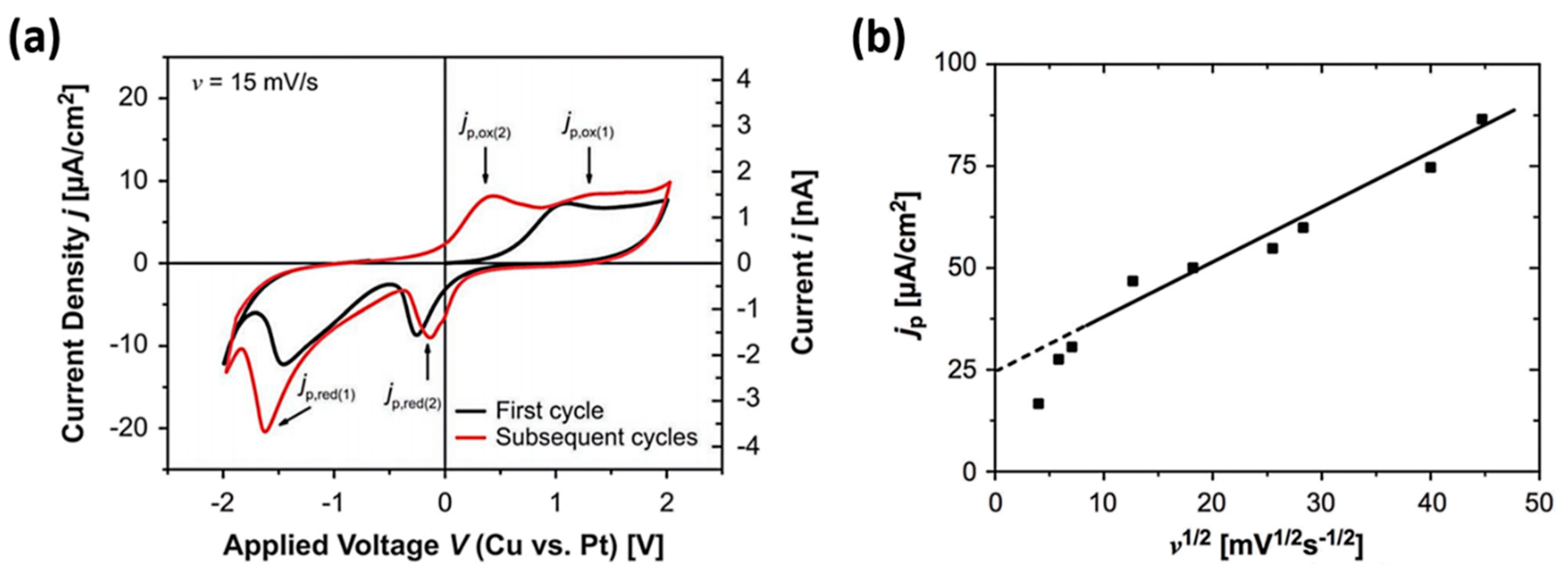
From a macro aspect, cyclic voltammetry (CV) measurements can be used to identify the redox reactions of the cations during resistive switching. The positive and negative ionic current peaks correspond to oxidation and reduction processes of cations, respectively. Figure 3a shows the redox process of Cu ions in a Cu/SiO2/Pt device [29]. The ionic current peak values are proportional to the square root of the voltage sweep rate (Figure 3b) [30], as the Randles–Sevcik equation expresses the peak current density
where is the number of transferring electrons during the redox reaction, is the concentration of the ions, and are the charge transfer coefficient and the diffusion coefficient of the ions, respectively, and is the sweeping rate.
From the microscopic perspective, Valov et al. [31,32] first reported the electrochemical Ag nucleation process at the atomic scale using the scanning tunneling microscope (STM) and it was found that Ag critical nucleus formation is the rate-limiting step. The nucleation rate J(s) is given based on the atomistic model for electrocrystallization by:
where () is applied cathodic potentials higher than , , , , and are the numbers of Ag+ ions and of active sites, Zeldovich factor, cathodic transfer coefficient and the Planck constant, respectively, stands for the number of atoms constituting the critical nucleus, is the transmission probability of an electron, is the free activation enthalpy of the charge transfer reaction (at ) and is the specific surface energy of the critical nucleus. Figure 4a,b show the STM images of the RbAg4I5 surface before and after the deposition of a cluster, and the smallest cluster was approximately 5 nm in diameter and 3 nm in height (Figure 4c). The dynamical change of shape, size, and position of nanoscale clusters in dielectrics with applied voltage were studied through in-situ transmission electron microscopy (TEM) by Yang et al. [33]. They can be affected by the kinetic parameters including ion mobility and redox rates, leading to four different filament growth modes and geometries (Figure 4d–g).
I: When the ion mobility and the redox rates are high, the cations can arrive the inert electrode, leading to the filament growing from the inert electrode and forming an inverted cone-shaped filament (Figure 4d) [34,35].
II: When and are low, the filament grows from the active electrode towards the inert electrode by cluster migration via the repeated splitting-merging processes (Figure 4e) [36].
III: When is low while is high, nucleation emerges inside the dielectric layer and the cations are reduced onto the cathode side of the nuclei, leading to the connection of the nuclei and the active electrode. Repeating of the process induces an effective forward growth towards the inert electrode (Figure 4f) [33].
IV: When is high while is low, nucleation only occurs at the counter electrode but the limited ion supply leads to branched filament growth towards the active electrode (Figure 4g) [36].
In short, the nucleation sites and the direction of the filament growth are determined by the ion mobility , while the ion supply and the geometry of the filament lie on the redox rates . Significantly, different filament growth modes can occur in the same device through tuning growth dynamics carefully as shown in the Figure 4h–l [33]. For instance, the initial growth mode of filament is the step-by-step bootstrapping Ag cluster (Figure 4h–k) in the device Ag/SiO2/W. Afterwards, a newly cone-shaped filament is formed with much wider base lying at the W cathode electrode side (Figure 4l), implying transition of filament growth mode from I to II.
The switching kinetics are essentially affected by ionic processes on the very nanoscale. Nanofilament can be reversibly formed and annihilated by electric field induced ions migration. Especially, when, during the process of forming or breaking the filament with lateral dimension being comparable to the Fermi wavelength and even smaller than the mean free path of electrons [37,38]. In this case, a quantum point contact is formed by just one atom, or just a few atoms and charge carriers can transport ballistically without any scattering leading to quantum conductance [39,40] in the unit of G0 = 2e2/h (where e is the electron charge and h is the Planck’s constant).
2.2. Dynamic Process of Native Oxygen Ions in Oxide-Based VCM Device
In the VCM device consisting of electrochemically inert anode/cathode electrodes and oxide dielectric, the active species, participating in electrochemical processes and redistribution, are native oxygen ions or oxygen vacancies inside the oxide-based electrolytes. The high electric field could break the bonds between oxygen and metal, which transform into oxygen ions and metal cations. Under the electric field, oxygen ions leave their lattice sites and created VOs in the switching layer, as indicated by the oxygen exchange reaction [41]
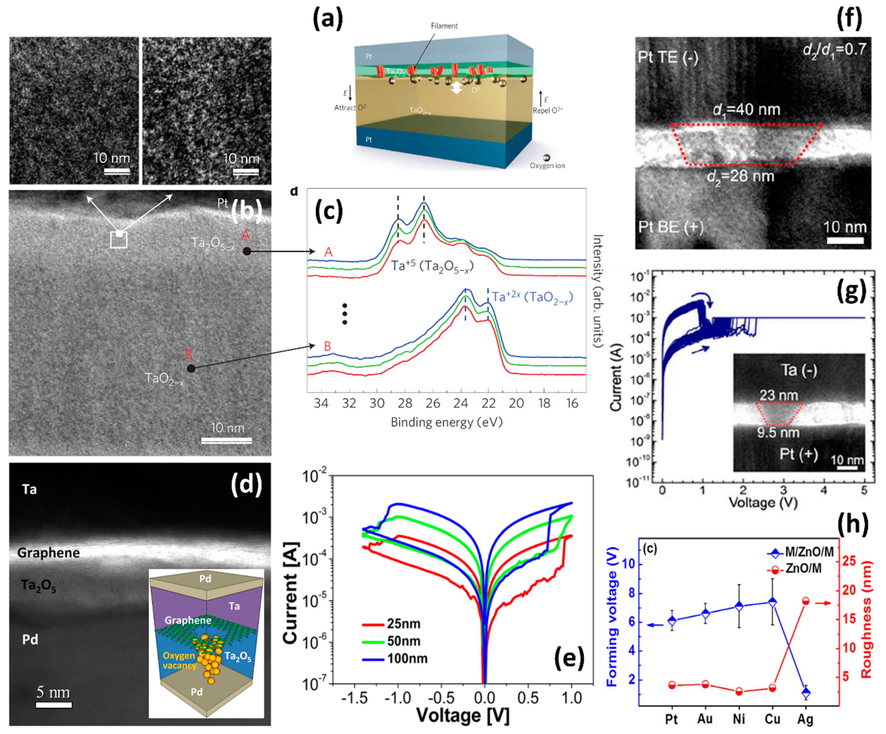
where and denote oxygen ions of the lattice sites and oxygen vacancies, respectively, which induces the formation of a conducting suboxide filament. The metal cation in the oxide is reduced to a lower valence state (Forming/Set process) and the subsequent being oxidized back to the near-stoichiometric oxide composition (Reset process) (Figure 5a) [28,42]. The formation and annihilation of conductive nanopaths were observed in the Pt/ZnO/Pt device (Figure 5b,d) by Chen et al. [43] due to the migration of oxygen ions and redox process using in-situ TEM. The electrochemical redox reaction is given by:
In addition, the components of the nanofilament and ruptured area were identified as the Zn-dominated ZnO1−x (Figure 5c) and the ZnO (Figure 5e), respectively, through in-situ high resolution TEM (HRTEM) measurement. Kwon et al. [44] probed directly stable oxygen-deficient Ti4O7 (Magnéli phase) conical shape nanofilaments with diameters of 10 (top) and 5 nm (bottom) (Figure 5f) after an electroforming process which induces oxygen ions migration with VOs concentration increasing in the Pt/TiO2/Pt device. The phase structure of the nanofilament transformed from Magnéli into anatase (stoichiometric phases) during the Reset process, when the oxygen ions were supplied to suboxide nanofilament from the neighboring TiO2 (Figure 5g). Similarly, Xue et al. [45] also found that new phase of VO2 nanochannels can be constructed in V2O5 matrix by electric field induced oxygen ions migration process (Figure 5h). In VCM devices, oxygen-deficient nanofilament can be constructed in the dielectric by electric field induced native oxygen migration. By taking advantage of synchrotron-based nanobeam X-ray fluorescence, Miao et al. identified the formation of filaments consist of an amorphous Ta(O) solid solution with a decreasing oxygen content in TaOx memristors [4]. By using scanning transmission synchrotron X-ray spectromicroscopy (STXM), Williams et al. directly observed the formation of a localized oxygen-deficiency-derived conductive channel surrounded by a low-conductivity ring of excess oxygen in the hafnium oxide memristors [46]. Furthermore, oxygen-deficient nano-filaments are also directly identified employing a CS-corrected transmission electron microscope in HfOx memristors by Yang et al. [47].
Direct microscopic detection of oxygen ion motion at the nanoscale is vital for disclosing mechanisms of memory, optimizing storage performances and developing applications of VCM devices. Unfortunately, detecting the migration of oxygen ions and consequent growth/dissolution of oxygen-deficient nanofilaments are challenging, due to the low atomic number of oxygen element and the fact that the normally used electron microscopy imaging mainly utilizes the mass attribute of ions. Some notable progresses about detection of oxygen ion motion were made recently using the charge properties of ions. Kang et al. [48] directly observed oxygen vacancy nanofilament evolution in the HfOx film by in-situ electron holography through detecting the electrostatic potential distribution and low-energy-filtering that can reflect the oxygen concentration changes. Figure 6a shows the phase featuring that indicates the electric potential evolutions during the Forming and Reset processes with applied positive (7 V) and negative (−6.5 V) voltages, respectively. The negative potential is due to the electron transport in the migration path and can used for tracking the evolution of the oxygen vacancies nanofilament. Also, the low-energy-filtered images confirm that oxygen concentration is reduced in the forming process (Figure 6b), which indicates the removal of the oxygen ions from the HfOx matrix with the VOs formation. Yang et al. [47] verified the migration and accumulation of oxygen ions in HfO2-based memristor by brilliantly utilizing in-situ electrostatic force microscopy (EFM) measurements where the 1ω and 2ω (Figure 6d,e) components of the electrostatic force gradient between the probe and the conductive atomic force microscopy (C-AFM) stimulated (different voltages) region (Figure 6c) indicate the charges accumulation and structural distortions, respectively. These results show oxygen ion migration and accumulation in HfO2 matrix. The evolution dynamics of oxygen ion migration inducing oxygen-deficient nanofilaments were shown in Figure 6f. When positive bias is applied through the tip, the oxygen ions migrate to the anodic interface with oxygen vacancies accumulating from the cathodic interface to the anodic interface (the formation of the oxygen-deficient nanofilaments). Subsequently, applying reversible bias can drive oxygen ions moving back into the oxide, resulting in the dissolution of the existing nanofilament. Other simple and efficient approaches, which can identify the oxygen ion motion at the atomic scale, are to be developed to further understand dynamic processes of oxygen ions for providing a more general understanding of the oxygen-deficient nanofilaments evolution in the oxide-based memristor.
2.3. Dynamic Process of Other Active Ions
2.3.1. Native Active Ions from Dielectric
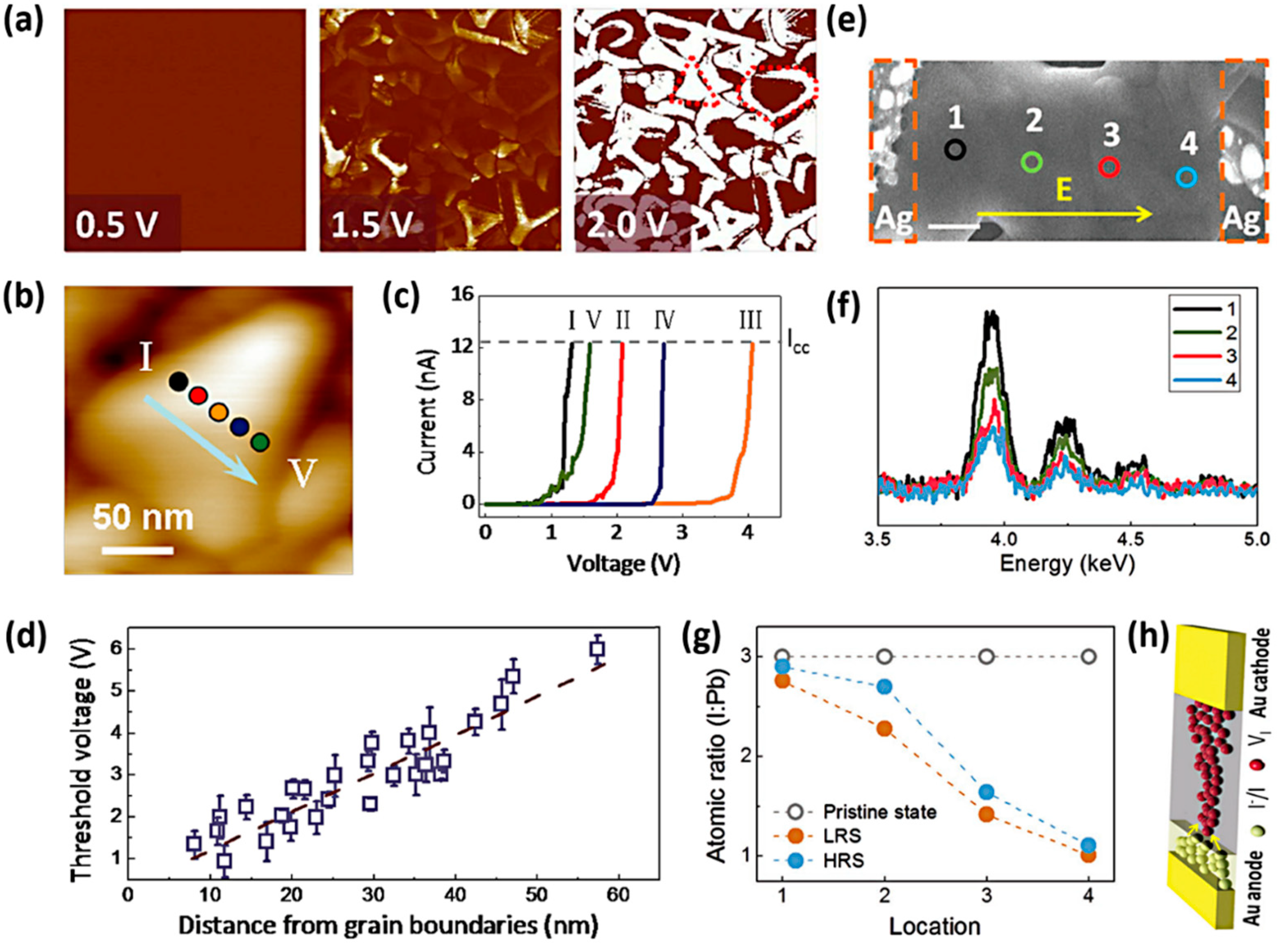
In some sandwiched devices, anion/cation from the intermediate dielectric (e.g., LiCoO3, CH3NH3PbI3, and MoS2) can migrate under electric field, which may be an obstacle to practical applications. So, understanding and control of the ion generation and migration will not only improve device performances but also develop new device concepts. Zhu et al. directly observed the lithium ions movement in LixCoO2 [49], as well as clarified the transport of iodine ions with lower activation energy and formation/annihilation of iodine vacancies nanofilaments in CH3NH3PbI3 [50,51] under the electrical field. The Li-ion can preferentially migrate in the grain boundary of the LixCoO2 nanocrystal (Figure 7a), being attributed to a low Li-ion diffusion energy barrier through high-density defects. Besides, the conductivity is directly correlated to the location of the measurement spots on the LixCoO2 grain, wherein the grain boundary regions were more conductive (I and V) than the interiors of the grain (Figure 7b,c). The switching threshold voltages shows a close linear relationship with the distance from grain boundaries (Figure 7d), which indicates that Li ions can be extracted more easily from the LixCoO2 grain boundary. On the other hand, in the electroformed devices with CH3NH3PbI3, I intensity gradually decreased from the anode to the cathode (1, 2, 3, and 4 locations) (Figure 7e,f) with I:Pb ratio reducing to 1 near the cathode (at location 4) (Figure 7g), which illustrates the I ions movement into the anode/CH3NH3PbI3 interface and VI nanofilament being formed (Figure 7h). Sangwan et al. [52,53] stated that sulfur ions can transport along grain boundaries in single-layer MoS2-based memristor, leading to the increase of sulphur vacancy concentrations with resistance decreasing. However, a direct observation experiment of the sulfion ions migration will be needed at the atomic scale in the layered transition metal chalcogenides-based memristor.
2.3.2. Active Cations from Ion Gel in Three-Terminal Electrochemical Transistors
The insertion and extraction of the ions (e.g., Li+, H+), located in the electrolytes, to/from the functional layer can modulate memory characteristics and enrich device functionalities [54,55]. So, studying and understanding the evolution and control of ions in the dielectric under electrical bias are critically important for the reliable applications (e.g., neuromorphic computing). Yang et al. [56] realized reversible intercalation of active Li ions from gate electrolytes into layered 2D α-MoO3 lattice through gate voltages induced electrochemical doping in three-terminal electrochemical transistors (ECT) as electronic synaptic devices. When a positive gate voltage was applied, Li ions from the solid electrolyte accumulated on the MoO3 channel surface in the beginning. Then, they were injected into the interior (Figure 8a) to form LixMoO3 compound inside the MoO3 channel, leading to electrochemical doping and modulating of the conductance of the device. Electrochemical doping can be expressed as:
where x is the number of injected Li ions. It can be found that the valence of Mo ions changes from 6+ to 5+. On the contrary, a negative gate voltage can fully extract the Li ions from the MoO3 channel into the electrolyte (Figure 8b) with the channel conductance returning initial value. The extracting electrochemical process can be expressed as:
The dynamical evolution process of Li ions migration was further studied by Huang et al. [57] through systematic cross-sectional TEM observations on a 3-terminal transistors with a WSe2 channel and Li ion gel gate, which implements the drifting or attraction of Li ions to/from the channel under the voltage pulses. When a one-time voltage pulse was applied on the device, the crystal structure of WSe2 channel was almost invariant (Figure 8c,d) as Li ions are just adsorbed on the surface of the WSe2 channel (Figure 8e) and readily diffusing back into the ion gel after the removal of voltage supply. This electrical transport behavior can be used as short-term plasticity (STP) in synaptic mimicking. In contrast, when successive voltage pulses were applied, clear structure disorders in the WSe2 lattice were observed (Figure 8f,g), indicating that Li ions already intercalated into the WSe2 lattice (Figure 8h) [58,59,60]. Furthermore, these embedded Li ions hardly diffuse back to the ion gel spontaneously after removing the voltage, which resembles the long-term plasticity (LTP) of a biological synapse.
Injection of H ions from ionic liquid (IL) electrolyte in the WO3 epitaxial films was studied by Jin et al. [61], which can modify the transport behaviors of device. Under a low positive gate voltage (VG), the anions (TFSI−) and cations (DEME+) in IL accumulate at the IL/gate and IL/channel interfaces respectively to form electric double layers (EDLs) (Figure 8i), which introduces the concentration of electrons in the semiconductor channel and decreases the device resistance. Once VG is removed, the resistance will recover by the ion relaxation. If applied VG is higher than the hydrolysis reaction threshold voltage (VT), water molecules in IL dissociate into protons and hydroxyls, with which the protons can be inserted into WO3 to cause valence change from W6+ to W5+ and forms a stable HxWO3 phase (Figure 8j) with nonvolatile resistance decreasing. The protons can dope at the A-sites of WO3 that provide ample interstitial space for ion intercalation and extraction.
Currently, researchers often utilized single ionic species (e.g., Li+, H+) from ion gel to modify device properties. The electric field induced dual-ion modulation needs further research and development, which is more interesting and may achieve wider functionalities.
2.4. Switching Mechanisms in Organic Devices
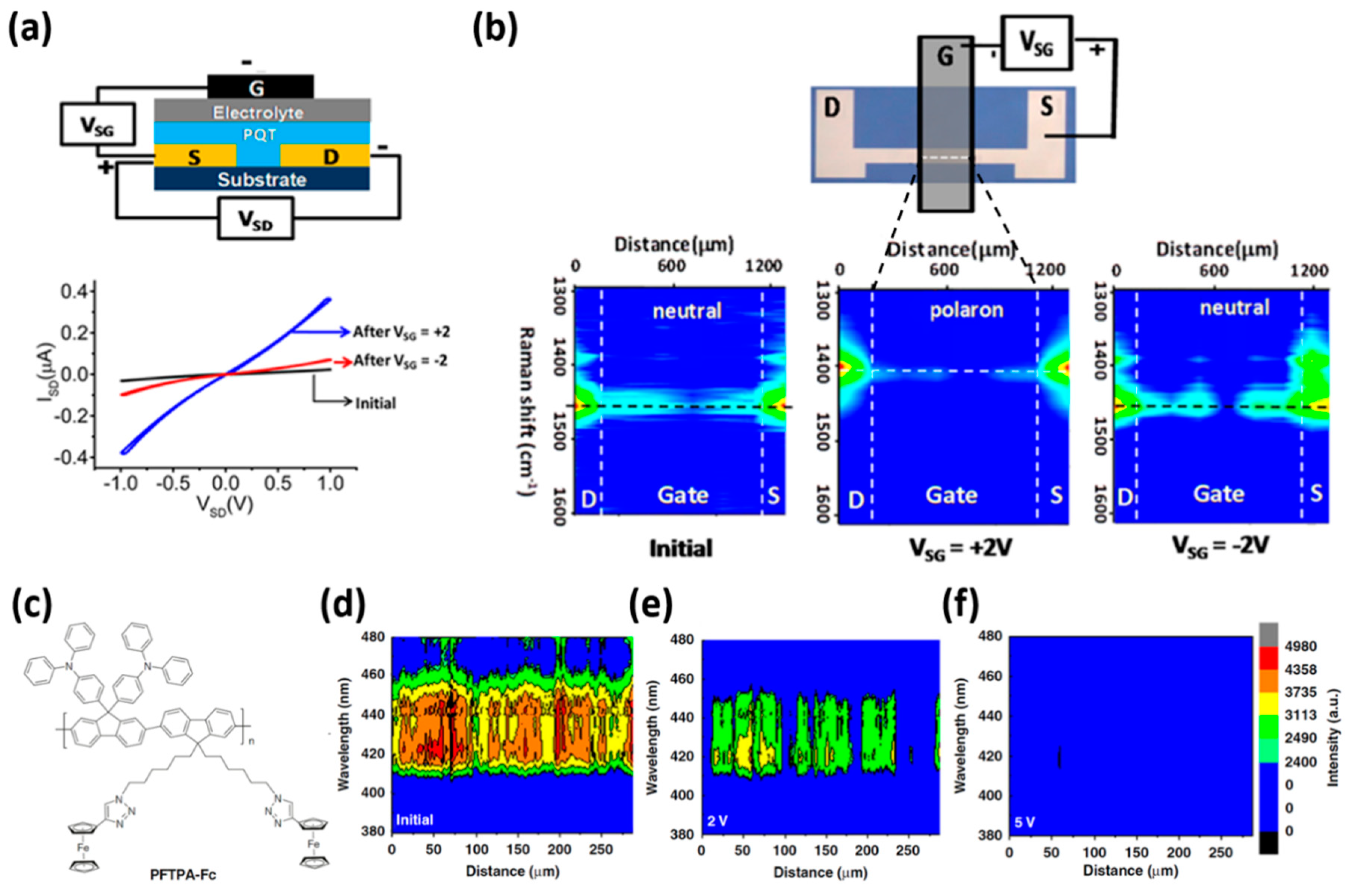
Organic materials including small molecules, polymers and hybrid materials have advantages of low-cost potential, easy processability and chemical tunability and designability, etc. [7,62,63] Many studies have been conducted on mechanistic understanding in the organic-based memristor with intrinsic and extrinsic mechanisms [64,65,66,67,68,69,70], in order to optimize the composition and design of organic materials for commercial translation. The extrinsic mechanisms are active metal electrode ions injecting into organic materials [71,72,73,74], while the intrinsic mechanisms are even more striking, including the charge transfer between the electron donating and accepting [68,75], electrochemical redox reaction [64,66,67,69], and conformational change [65,70]. Some advanced approaches have been exploited to study conduction mechanisms in the organic materials-based memristors, e.g., the in-situ Raman mapping and fluorescence measurements. Understanding the primary driving mechanism in organic resistive memory devices is a challenge and requires in-situ molecular characterization for such devices. Some advanced approaches have been exploited to study conduction mechanisms in the organic materials-based memristors. For example, by constructing a three terminal polythiophene device, McCreery et al. [76] performed direct observation of the working memory device with spatially resolved Raman spectroscopy, and provided direct correlation of conductivity changes with generation of conducting polarons in the polythiophene layer. Polarons are radical cation that formed by losing unbonded electrons from the sulfur atom on the polythiophene during electric field-driven redox reaction process. The source (S)-drain (D) conductivity, which is quite small at initial state, increase significantly after a VSG = +2 V due to formation of conducting polarons in the channel region. At a bias of VSG = −2 V, the remaining polarons were reduced back to their neutral state, resulting in small SD current (Figure 9a). The Raman line scans across the gate region (Figure 9b) indicates that in the initial state the Raman peak at 1460 cm−1 corresponds to the neutral PQT is prominent. However, when a SG bias of 2 V was applied, the main Raman signal intensity from the entire S to D region shifts to the 1405 cm−1 position. The oxidation is reversible, with most of the charged PQT along the SD line reduced back to neutral PQT upon reversal of the bias to VSG = −2 V. This observation provides a direct correlation of polaron generation with device conductivity. Zhang et al. [77] investigated the spatial evolution of the oxidative states of the ferrocene pendant triphenylamine (TPA) and ferrocene (Fc) (PFTPA-Fc) thin film under different applied voltages through fluorescence line scans. Strong emission appeared in the wavelength range of 410–460 nm in initial state with emissions between 430 and 460 nm and between 415 and 430 nm corresponding to Fc and TPA, respectively (Figure 9c). The Fc fluorescence signals attenuates significantly under applied smaller voltage (2 V) (Figure 9d), illustrating that the ferrocene (Fe2+) moieties are partially oxidized into ferrocenium (Fe3+). The TPA emission also weakens under higher voltage (5 V) (Figure 9e), indicating TPA being oxidized. These results state the multilevel electrochemical redox behaviors of the solid-state PFTPA-Fc thin film.
Although excellent work has been reported to reveal an in-depth understanding of the resistive switching mechanism in some organic materials, the complex structures of organic materials still make the general mechanisms of organic-based memristors yet to be further explored to design organic devices with superior performance for commercial translation. For example, the intrinsic factors that are responsible for each important switching parameter of memristors, such as the threshold voltage, hysteresis, thermal stability, and repeatability, are not well understood. Besides, constructing commercial memristor device demands extra ingredients including the ability to form uniform thin film, good mechanical stability, acceptable cell-to-cell uniformity, etc., wherein the underlying mechanisms are scarcely investigated.
3. Influence Factors of Memristive Performances and Optimization Methods
Memristive performances, consisting of uniformity, endurance, power consumption, switching speed and switching voltage values, are affected by many factors including the electrode types, interfaces between electrodes and switching materials, ambient atmosphere (e.g., oxygen and water molecules) and dielectric materials. Besides, the bias scheme, such as the voltages and time employed to program, erase, and read the devices would also be very critical. Memristive performances can be significantly improved by modulating these factors.
3.1. Electrode Engineering
As an integrated and important part of the sandwiched memristors, the memristive performances can be significantly affected by the electrode materials (intrinsic effect and configuration of electrode by designing structured electrodes). For example, high electronegativity and large ionic size (Pt, Au) possess larger OFF/ON ratios and Set voltages (Figure 10a,b) [78], which can be attributed to the lack of the leaking sites in the Pt/Au devices as foreign metallic species and the larger ionic radius leading to a lower activation barrier for diffusion. Yang et al. [33] found that devices with different metal electrodes require different electric fields to drive ions for nanofilament formation. For example, the electrochemical process of Ag ions in SiO2 is the easiest and requires a smaller electric field of <1 MV/cm−1 than Ni and Pt (3–5 MV cm−1). This can be ascribed to the polarizability increasing in the series Ag→Ni→Pt, as well as higher charge numbers and sizes of Ni and Pt ions [78], which leads to their diffusion being difficult in switching layers. As such, Ag−/Cu− species can transport more easily in dielectrics [38] (especially Si [79]), which introduces defect centers into the integrated silicon circuitry [80]. Guha et al. [79] employed first principles calculations for estimating diffusion barriers of active ions in HfOx. It is identified that Sn possesses a slower diffusion barrier without creating active defects, which reduces contamination risk than Cu and Ag. Besides, Sn-based devices show very fast and steep-slope memory switching, making itself a very good choice as CMOS compatible electrode material.
Carefully designing asymmetric devices can significantly improve memristive performances. Chen et al. [80] systematically studied the resistive switching characteristics including VSet/VReset and OFF/ON ratios of TE (Ni, Co, Al, Ti, Zr and Hf) /Ta2O5/Pt memristors. The Al/Ta2O5/Pt and Ti/Ta2O5/Pt devices show the best memristive properties with very concentrated distributions and appropriate amplitudes of all parameters. These results are contributed by oxygen affinities of Ti and Al being comparable to that of Ta, which will lead to forming the thin interfacial layers served as reservoirs of oxygen ions and producing an appropriate amount of VOs accelerating the Set process. Therefore, it is better to choose the metal electrodes with comparable oxygen affinities to the metal in the dielectric layer. This rule also explains excellent endurance in the TiN/TiO2/Pt (>106 cycles) [81], Hf/HfO2/TiN (>1010 cycles) [82] and Ta/TaOx/Pt (>1010 cycles) [83] memristors.
The configurations of electrode were also considered in some studies to modulate electric field for improving memristive performances. Shin et al. [84] designed a structured electrode to realize local enhancement of electric fields and controllable formation of nanofilament. Ag pyramid electrodes were prepared in the Ag/Al2O3/Pt devices, causing the nucleation and growth of Ag nanofilaments at the tip of the pyramid (Figure 10c) with highly enhanced electric fields (Figure 10d). Low and reliable switching voltages were obtained, and the endurance and retention of the device are highly improved [84]. Qian et al. [85] inserted gold nanoparticles between the switching layer (amorphous Si) and inert electrodes to modify electric field distribution and control the growth of the nanofilament (Figure 10e) with great improvement of memristive performances (lower electroforming voltage and higher OFF/ON ratio) [85]. These electrode engineering strategies can be used to well improve the switching properties.
3.2. Interface Engineering
Interface engineering mainly means inserting an additional thin film at the interfaces between electrodes and switching layers or modifying morphology of interfaces to improve the performances of memristors. The additional thin films include AlOx [86,87,88,89,90] resistors and structure-defective graphene [91,92]. For example, Chen et al. [88] obtained a lower operating current memory device TiN/Si/V:SiO2/Pt by inserting a α-Si thin layer at the TiN/V:SiO2 interface and Si thin layer being oxidized to SiOx during Forming/Set process as series resistor of the SiO2. Also, Cho et al. [86] utilized the formation of AlOx layer through oxidation of Al layer by O2 plasma treatment at the PI:PCBM/Al interface to enlarge OFF/ON ratios and reduce operating current in the Al/PI:PCBM/Al devices. Lee et al. [89] designed an asymmetric TaOx-based memristor Pt/Ta2O5/TaOx/Pt to localize resistance switching (Figure 11a) and obtained high switching-speed (10 ns), good endurance (>1012 cycles), good retention (more than 10 years at 85 °C) and lower power-consumption performances. HRTEM and X-ray photoelectron spectroscopy (XPS) show that in Pt/Ta2O5−x (the lighter colour) /TaOx (the darker colour) /Pt device (Figure 11b,c) the metal Ta clusters in the Ta2O5−x layer account for the good device endurance characteristics. Lu et al. [91] optimized the device performance by inserting a structure-defective atomic thickness graphene with nanopores to block the oxygen ions migration and redox reaction processes at the nanoscale in the Ta/graphene/Ta2O5/Pd devices (Figure 11d). The engineered controlling of the graphene nanopore size can effectively modulate the device performance (Figure 11e).
The configuration of the interface can also be changed to modulate and optimize the memristive properties. Gao et al. [90] constructed cone-shaped nanofilaments by using an active Ta metal cathode to improve switching uniformity (Figure 11g). Not like showing in the Pt/Ta2O5/Pt device (Figure 11f), Ta metal can be oxidized spontaneously, which can produce a hazy interface between the cathode and Ta2O5 film as a load resistor to inhibit the overgrowth of nanofilaments. Furthermore, Xue et al. [77] found the forming voltages of the switching devices strongly depend on the roughness of the interface between electrode and switching layer. The smaller forming voltage/free forming process can be obtained in memristors with rougher interface (Figure 11h) [77]. Furthermore, if the rough interfaces are introduced with a controllable manner such as by using lithography, the device performance will be greatly improved without introducing complex device integration.
3.3. Ambient Atmosphere
Ambient atmosphere (e.g., oxygen and water species) has a strong effect on the switching properties [93,94,95,96]. Studying and clarifying the atmosphere effects is an urgent need for understanding the microscopic details of electrochemical reactions during resistive switching and improving switching characteristics. N. Knorr et al. [97] firstly demonstrated that threshold voltages decreased for higher relative humidity (RH) ascribed to the field-induced absorption of ambient water. And, the formation of metallic cations was promoted by the redox of water providing the counter charge supply needed for the ionization of metal [98]. Waser et al. [99] found the electrocatalytic release and reincorporation of oxygen at the Pt/SrTiO3 interface as follows:
which causes the resistance change with large OFF/ON ratio. Rupp et al. [26] stated that the memristive behaviors occur at ambient humidity, but vanish in dry atmosphere in the Pt/SrTiO3-δ/Pt device via cyclic voltammetry. This phenomenon is due to the adsorbed surface water molecules that change the Schottky barrier and the charge transfer in the oxide layer. Valov et al. [27] investigated in detail the effects of the humidity on resistive switching through isotope labeling experiments (Figure 12a) combined with time-of-flight secondary-ion mass spectrometry (ToF-SIMS). It is identified that oxygen, from water molecules or oxygen molecules, is injected into the SrTiO3 layer during the switching operation and influences switching characteristics of SrTiO3-based memristor. 18O− intensity increases near the Pt/SrTiO3 interface after cycling 60 times in N2/H218O atmosphere (Figure 12b), which means 18O is incorporated from the atmosphere into SrTiO3 during switching process. Besides, the endurance of device was improved in humid N2/H218O atmosphere (over 2000 cycles) than that in dry N2 (switching failure after 1000 cycles). The electrochemical Set and Reset processes are as follows:
Therefore, the effects of the humidity on the memristive properties and mechanisms should be considered at air condition.
3.4. Selection of Dielectric Materials
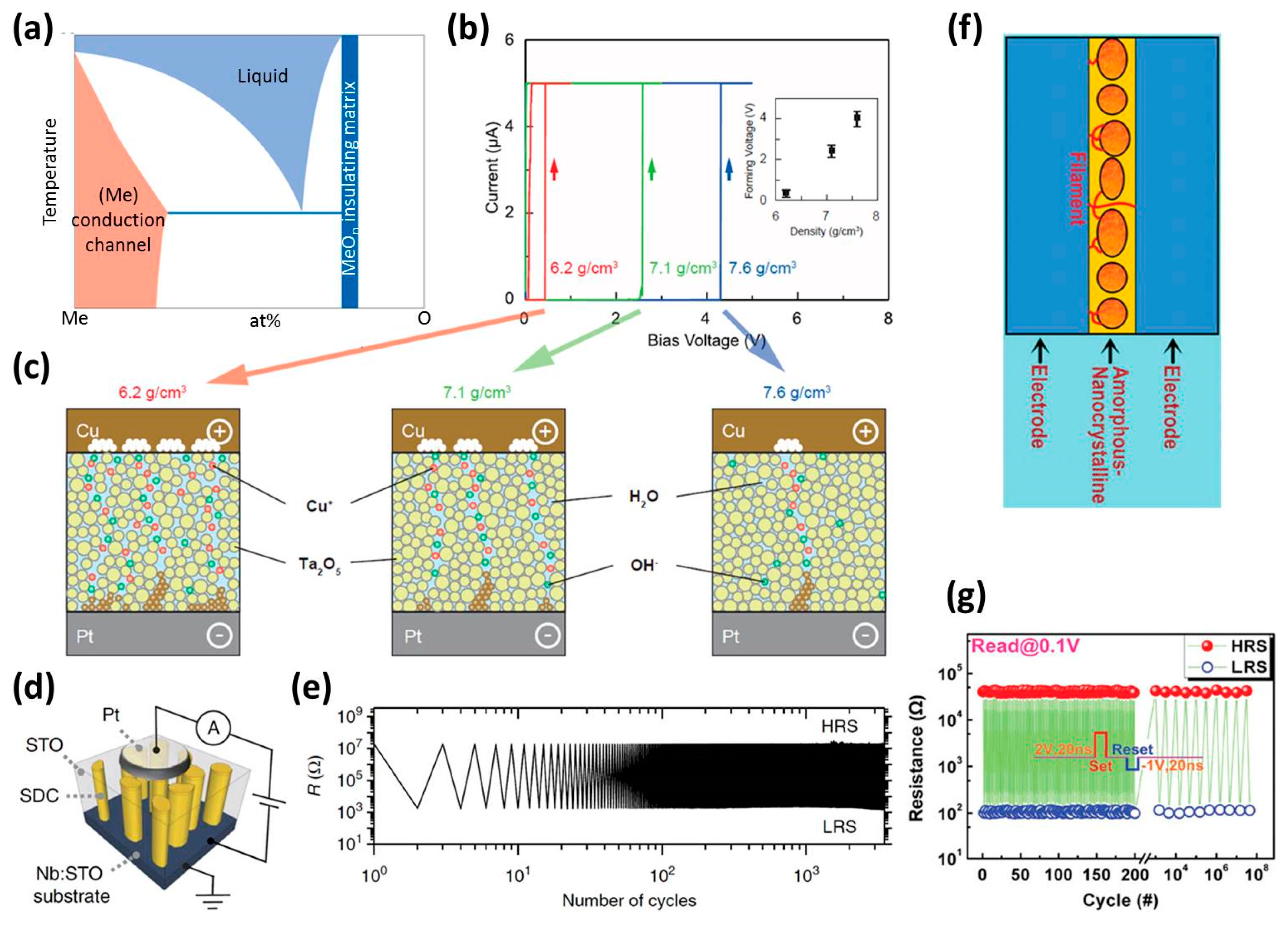
A very large amount of switching materials including oxides, nitrides, tellurides, selenides, amorphous Si, and 2D materials have been reported to date. So, which materials should be selected to get excellent memristive performances? Yang et al. [100] proposed a switching material selection criteria that reliable switching requires a simple material system with only two thermodynamically stable solid-state phases of insulating (MeOn) and conductive (Me) phases, which serve as the switching matrix and conduction nanofilament, respectively. The two phases should not react with each other to form a new phase by Joule heating in the phase diagram, while the conductive phase should also have a large solubility of oxygen (Figure 13a) to accommodate mobile oxygen species during switching. As simple and promising material systems, TaOx and HfOx-based devices have been reported having reliable switching characteristics with over trillion cycles for TaOx [89] and ten billion switching cycles for HfOx [101]. Other material systems satisfying the switching material selection criteria described above should also have outstanding electrical performances.
It is worth noting that the configuration of the switching materials is also an important factor to optimize the memristive performances [102,103,104,105]. Aono et al. [106] explored the impact of Ta2O5 film density on the forming process. When the density of the Ta2O5 film is decreased, the forming voltage is reduced in the Cu/Ta2O5/Pt device (Figure 13b,c). Moreover, self-assembled Sm-doped CeO2 (SDC) and SrTiO3 (STO) switching media [107] (Figure 13d) can control ions drifting to precisely engineer the resistance states with large OFF/ON ratios (~104) and high reproducibility (over 103 cycles) (Figure 13e). Shang et al. [108,109] fabricated an amorphous-nanocrystalline hafnium oxide thin film that can confines the formation of the nanofilament (Figure 13f) to produce reproducible (over 1000 consecutive cycles) resistive switching behavior (Figure 13g). The layered two dimensional (2D) materials can control ion migration to produce excellent memristive properties [110], e.g., free of forming [111], good thermal stability (340 °C) and endurance (over 107 cycles) [112], larger OFF/ON current ratios (106) and lower programming currents/voltages (less than 1 μA/0.1–0.2 V) [113,114]. These results demonstrate that 2D materials are achievable as promising switching layers in the memristor. However, high-quality (less impurities, cracks, and wrinkles introduced during transfer) and complementary metal-oxide semiconductor (CMOS) compatible 2D materials needs to be developed [115].
Overall, the selection and configuration of the switching matrixes are of importance in understanding and controlling switching behavior.
3.5. Bias Scheme
Improved performance during the programming, erasure, and reading of the memristors relies largely on the voltage bias scheme, which confines the shape, distribution, and location of the nanofilaments. For example, Yin et al. [116] proposed a ramped-pulse series operation method to improve switching stability and cycling endurance. They also found that the dispersion of VReset could be minimized by optimizing the amplitude of pulse. Hou et al. [117] found that Roff strongly affects the Set speed and disturb immunity, which cannot be improved simultaneously by monotonously variation of Roff, such Set speed-disturb dilemma demonstrates the importance of accurately controlling the distributions of resistance in the memristor [118].
4. Applications
Memristors have shown great potential in a variety of applications such as biologically inspired computing [11,13,14,15,16,17,18], in-memory computing [8,9,10,11,12], and the unique functionality of memristors [21,119,120,121] past the von Neumann and Moore’s law era. A compact and efficient parallel computing technology can be offered by the memristors, which is applicable to artificial neural networks and high-performance machine learning. In-memory computing can directly process data in the memory, which can enable area- and energy-efficient computation and address memory walls. More memristive applications are emerging including hardware-intrinsic security utilizing underlying stochastic operation (e.g., nonlinear conductance variations of memristors [119] and stochastic delay time of threshold switching), provable key destruction leveraging reconfigurability and variability of memristors [120], and partial differential equation solvers for performing high-precision computing tasks [121].
5. Summary and Perspectives
Over the past decade, great efforts have been devoted to understanding, optimizing, and applying memristors. Through field-driven ionic processes, atomic-level ion movement and electrochemical reaction, the device resistance is modulated reconfigurablly. A number of factors including the electrode, interface between electrode and switching layer, ambient atmosphere, the configuration of switching matrix and bias scheme can all affect memristive switching performances. All these factors need to be considered carefully to optimize device properties used as on-chip memory and storage, biologically inspired computing and in-memory computing. Nevertheless, under extreme conditions (e.g., ultrahigh frequency, ultra-small scale, and electromagnetic radiation), the atomic-level kinetics and thermodynamics of ion await to be investigated, aiming to pursuing the robust devices by developing new material and designing new device architecture. Besides, advanced and utilitarian simulation tools and analytical techniques with high spatial and temporal resolution at room temperature need to make breakthroughs for realizing real-time and nondestructive analysis of the reconfiguration dynamics at the atomic scale, which speeds up the material and device developments along with precise control of ions, ultimately achieve excellent comprehensive performances in a single device and expand its novel functional applications.
Author Contributions
Writing—original draft preparation, W.H.X.; writing—review and editing, G.L., X.-H.X. and W.H.X.; supervision, X.-H.X. and G.L.
Funding
We are grateful for the financial support of the National Natural Science Foundation of China (61434002, 61674153 and 61722407), the National Key R&D Program of China (2017YFB0405703 and 2017YFB0405604), and the Natural Science Foundation of Shanxi Normal University.
Conflicts of Interest
The authors declare no conflict of interest.
References
- Chua, L. Memristor-the missing circuit element. IEEE Trans. Circuit Theory 1971, 18, 507–519. [Google Scholar] [CrossRef]
- Strukov, D.B.; Snider, G.S.; Stewart, D.R.; Williams, R.S. The missing memristor found. Nature 2008, 453, 80–83. [Google Scholar] [CrossRef] [PubMed]
- Yang, Y.C.; Pan, F.; Liu, Q.; Liu, M.; Zeng, F. Ultrafast and high-density memory application. Nano Lett. 2009, 9, 1636–1643. [Google Scholar] [CrossRef] [PubMed]
- Miao, F.; Strachan, J.P.; Yang, J.J.; Zhang, M.X.; Goldfarb, I.; Torrezan, A.C.; Eschbach, P.; Kelley, R.D.; Medeiros-Ribeiro, G.; Williams, R.S. Anatomy of a nanoscale conduction channel reveals the mechanism of a high-performance memristor. Adv. Mater. 2011, 23, 5633–5640. [Google Scholar] [CrossRef] [PubMed]
- Li, C.; Han, L.; Jiang, H.; Jang, M.H.; Lin, P.; Wu, Q.; Barnell, M.; Yang, J.J.; Xin, H.L.; Xia, Q. Three-dimensional crossbar arrays of self-rectifying Si/SiO2/Si memristors. Nat. Commun. 2017, 8, 15666. [Google Scholar] [CrossRef] [PubMed]
- Pi, S.; Li, C.; Jiang, H.; Xia, W.; Xin, H.; Yang, J.J.; Xia, Q. Memristor crossbar arrays with 6-nm half-pitch and 2-nm critical dimension. Nat. Nanotech. 2018, 14, 35–39. [Google Scholar] [CrossRef] [PubMed]
- Gao, S.; Yi, X.; Shang, J.; Liu, G.; Li, R.W. Organic and hybrid resistive switching materials and devices. Chem. Soc. Rev. 2018. [Google Scholar] [CrossRef] [PubMed]
- Borghetti, J.; Snider, G.S.; Kuekes, P.J.; Yang, J.J.; Stewart, D.R.; Williams, R.S. ‘Memristive’ switches enable ‘stateful’ logic operations via material implication. Nature 2010, 464, 873–876. [Google Scholar] [CrossRef]
- Hasegawa, T.; Terabe, K.; Tsuruoka, T.; Aono, M. Atomic switch: Atom/ion movement controlled devices for beyond von-neumann computers. Adv. Mater. 2012, 24, 252–267. [Google Scholar] [CrossRef] [PubMed]
- Kumar, S.; Strachan, J.P.; Williams, R.S. Chaotic dynamics in nanoscale NbO2 Mott memristors for analogue computing. Nature 2017, 548, 318–321. [Google Scholar] [CrossRef] [PubMed]
- van de Burgt, Y.; Melianas, A.; Keene, S.T.; Malliaras, G.; Salleo, A. Organic electronics for neuromorphic computing. Nat. Electron. 2018, 1, 386–397. [Google Scholar] [CrossRef]
- Wong, H.S.; Salahuddin, S. Memory leads the way to better computing. Nat. Nanotech. 2015, 10, 191–194. [Google Scholar] [CrossRef] [PubMed]
- Ohno, T.; Hasegawa, T.; Tsuruoka, T.; Terabe, K.; Gimzewski, J.K.; Aono, M. Short-term plasticity and long-term potentiation mimicked in single inorganic synapses. Nat. Mater. 2011, 10, 591–595. [Google Scholar] [CrossRef] [PubMed]
- Zhu, L.Q.; Wan, C.J.; Guo, L.Q.; Shi, Y.; Wan, Q. Artificial synapse network on inorganic proton conductor for neuromorphic systems. Nat. Commun. 2014, 5, 3158. [Google Scholar] [CrossRef] [PubMed] [Green Version]
- Wang, Z.; Joshi, S.; Savel’ev, S.; Song, W.; Midya, R.; Li, Y.; Rao, M.; Yan, P.; Asapu, S.; Zhuo, Y.; et al. Fully memristive neural networks for pattern classification with unsupervised learning. Nat. Electron. 2018, 1, 137–145. [Google Scholar] [CrossRef]
- Wang, Z.; Joshi, S.; Savel’ev, S.E.; Jiang, H.; Midya, R.; Lin, P.; Hu, M.; Ge, N.; Strachan, J.P.; Li, Z.; et al. Memristors with diffusive dynamics as synaptic emulators for neuromorphic computing. Nat. Mater. 2017, 16, 101–108. [Google Scholar] [CrossRef] [PubMed]
- Li, C.; Belkin, D.; Li, Y.; Yan, P.; Hu, M.; Ge, N.; Jiang, H.; Montgomery, E.; Lin, P.; Wang, Z.; et al. Efficient and self-adaptive in-situ learning in multilayer memristor neural networks. Nat. Commun. 2018, 9, 2385. [Google Scholar] [CrossRef]
- van de Burgt, Y.; Lubberman, E.; Fuller, E.J.; Keene, S.T.; Faria, G.C.; Agarwal, S.; Marinella, M.J.; Alec Talin, A.; Salleo, A. A non-volatile organic electrochemical device as a low-voltage artificial synapse for neuromorphic computing. Nat. Mater. 2017, 16, 414–418. [Google Scholar] [CrossRef] [PubMed]
- Li, C.; Hu, M.; Li, Y.; Jiang, H.; Ge, N.; Montgomery, E.; Zhang, J.; Song, W.; Dávila, N.; Graves, C.E.; et al. Analogue signal and image processing with large memristor crossbars. Nat. Electron. 2017, 1, 52–59. [Google Scholar] [CrossRef] [Green Version]
- Zidan, M.A.; Strachan, J.P.; Lu, W.D. The future of electronics based on memristive systems. Nat. Electron. 2018, 1, 22–29. [Google Scholar] [CrossRef] [Green Version]
- Jiang, H.; Belkin, D.; Savel’ev, S.E.; Lin, S.; Wang, Z.; Li, Y.; Joshi, S.; Midya, R.; Li, C.; Rao, M.; et al. A novel true random number generator based on a stochastic diffusive memristor. Nat. Commun. 2017, 8, 882. [Google Scholar] [CrossRef] [Green Version]
- Yang, J.J.; Pickett, M.D.; Li, X.; Ohlberg, D.A.; Stewart, D.R.; Williams, R.S. Memristive switching mechanism for metal/oxide/metal nanodevices. Nat. Nanotech. 2008, 3, 429–433. [Google Scholar] [CrossRef]
- Waser, R.; Aono, M. Nanoionics-based resistive switching memories. Nat. Mater. 2007, 6, 833–840. [Google Scholar] [CrossRef]
- Valov, I. Redox-based resistive switching memories (ReRAMs): Electrochemical systems at the atomic scale. Chem. Electro. Chem. 2014, 1, 26–36. [Google Scholar] [CrossRef]
- Pan, F.; Gao, S.; Chen, C.; Song, C.; Zeng, F. Recent progress in resistive random access memories: Materials, switching mechanisms, and performance. Mater. Sci. Eng. R 2014, 83, 1–59. [Google Scholar] [CrossRef]
- Messerschmitt, F.; Kubicek, M.; Rupp, J.L.M. How does moisture affect the physical property of memristance for anionic-electronic resistive switching memories? Adv. Funct. Mater. 2015, 25, 5117–5125. [Google Scholar] [CrossRef]
- Heisig, T.; Baeumer, C.; Gries, U.N.; Mueller, M.P.; La Torre, C.; Luebben, M.; Raab, N.; Du, H.; Menzel, S.; Mueller, D.N.; et al. Oxygen exchange processes between oxide memristive devices and water molecules. Adv. Mater. 2018, 30, 1800957. [Google Scholar] [CrossRef]
- Lee, J.; Lu, W.D. On-demand reconfiguration of nanomaterials: When electronics meets ionics. Adv. Mater. 2017, 30, 1702770. [Google Scholar] [CrossRef]
- Tappertzhofen, S.; Mündelein, H.; Valov, I.; Waser, R. Nanoionic transport and electrochemical reactions in resistively switching silicon dioxide. Nanoscale 2012, 4, 3040. [Google Scholar] [CrossRef] [Green Version]
- Tappertzhofen, S.; Menzel, S.; Valov, I.; Waser, R. Redox processes in silicon dioxide thin films using copper microelectrodes. Appl. Phys. Lett. 2011, 99, 203103. [Google Scholar] [CrossRef] [Green Version]
- Valov, I.; Sapezanskaia, I.; Nayak, A.; Tsuruoka, T.; Bredow, T.; Hasegawa, T.; Staikov, G.; Aono, M.; Waser, R. Atomically controlled electrochemical nucleation at superionic solid electrolyte surfaces. Nat. Mater. 2012, 11, 530–535. [Google Scholar] [CrossRef] [PubMed]
- Valov, I.; Staikov, G. Nucleation and growth phenomena in nanosized electrochemical systems for resistive switching memories. J. Solid State Electrochem. 2012, 17, 365–371. [Google Scholar] [CrossRef]
- Yang, Y.; Gao, P.; Li, L.; Pan, X.; Tappertzhofen, S.; Choi, S.; Waser, R.; Valov, I.; Lu, W.D. Electrochemical dynamics of nanoscale metallic inclusions in dielectrics. Nat. Commun. 2014, 5, 4232. [Google Scholar] [CrossRef] [PubMed] [Green Version]
- Kozicki, M.N.; Park, M.; Mitkova, M. Nanoscale memory elements based on solid-state electrolytes. IEEE Trans. Nanotechnol. 2005, 4, 331–338. [Google Scholar] [CrossRef]
- Choi, S.J.; Park, G.S.; Kim, K.H.; Cho, S.; Yang, W.Y.; Li, X.S.; Moon, J.H.; Lee, K.J.; Kim, K. In situ observation of voltage-induced multilevel resistive switching in solid electrolyte memory. Adv. Mater. 2011, 23, 3272–3277. [Google Scholar] [CrossRef] [PubMed]
- Yang, Y.; Gao, P.; Gaba, S.; Chang, T.; Pan, X.; Lu, W. Observation of conducting filament growth in nanoscale resistive memories. Nat. Commun. 2012, 3, 732. [Google Scholar] [CrossRef] [Green Version]
- Terabe, K.; Hasegawa, T.; Nakayama, T.; Aono, M. Quantized conductance atomic switch. Nature 2005, 433, 47. [Google Scholar] [CrossRef]
- Nandakumar, S.R.; Minvielle, M.; Nagar, S.; Dubourdieu, C.; Rajendran, B. A 250 mV Cu/SiO2/W memristor with half-integer quantum conductance states. Nano Lett. 2016, 16, 1602. [Google Scholar] [CrossRef]
- Zhu, X.; Su, W.; Liu, Y.; Hu, B.; Pan, L.; Lu, W.; Zhang, J.; Li, R.-W. Observation of conductance quantization in oxide-based resistive switching memory. Adv. Mater. 2012, 24, 3941–3946. [Google Scholar] [CrossRef]
- Xue, W.; Gao, S.; Shang, J.; Yi, X.; Liu, G.; Li, R.-W. Recent Advances of Quantum Conductance in Memristors. Adv. Electron. Mater. 2019. [Google Scholar] [CrossRef]
- Waser, R.; Dittmann, R.; Staikov, G.; Szot, K. Redox-based resistive switching memories—Nanoionic mechanisms, prospects, and challenges. Adv. Mater. 2009, 21, 2632–2663. [Google Scholar] [CrossRef]
- Sharath, S.U.; Vogel, S.; Molina-Luna, L.; Hildebrandt, E.; Wenger, C.; Kurian, J.; Duerrschnabel, M.; Niermann, T.; Niu, G.; Calka, P.; et al. Control of switching modes and conductance quantization in oxygen engineered HfOx based memristive devices. Adv. Funct. Mater. 2017, 27, 1700432. [Google Scholar] [CrossRef]
- Chen, J.Y.; Hsin, C.L.; Huang, C.W.; Chiu, C.H.; Huang, Y.T.; Lin, S.J.; Wu, W.W.; Chen, L.J. Dynamic evolution of conducting nanofilament in resistive switching memories. Nano Lett. 2013, 13, 3671–3677. [Google Scholar] [CrossRef] [PubMed]
- Kwon, D.H.; Kim, K.M.; Jang, J.H.; Jeon, J.M.; Lee, M.H.; Kim, G.H.; Li, X.S.; Park, G.S.; Lee, B.; Han, S.; et al. Atomic structure of conducting nanofilaments in TiO2 resistive switching memory. Nat. Nanotech. 2010, 5, 148–153. [Google Scholar] [CrossRef] [PubMed]
- Xue, W.; Liu, G.; Zhong, Z.; Dai, Y.; Shang, J.; Liu, Y.; Yang, H.; Yi, X.; Tan, H.; Pan, L.; et al. A 1D vanadium dioxide nanochannel constructed via electric-field-induced ion transport and its superior metal-insulator transition. Adv. Mater. 2017, 29, 1702162. [Google Scholar] [CrossRef]
- Kumar, S.; Wang, Z.; Huang, X.; Kumari, N.; Davila, N.; Strachan, J.P.; Vine, D.; Kilcoyne, A.L.D.; Nishi, Y.; Williams, R.S. Conduction channel formation and dissolution due to oxygen thermophoresis/diffusion in hafnium oxide memristors. ACS Nano 2016, 10, 11205. [Google Scholar] [CrossRef] [PubMed]
- Yang, Y.; Zhang, X.; Qin, L.; Zeng, Q.; Qiu, X.; Huang, R. Probing nanoscale oxygen ion motion in memristive systems. Nat. Commun. 2017, 8, 15173. [Google Scholar] [CrossRef] [Green Version]
- Li, C.; Gao, B.; Yao, Y.; Guan, X.; Shen, X.; Wang, Y.; Huang, P.; Liu, L.; Liu, X.; Li, J.; et al. Direct observations of nanofilament evolution in switching processes in HfO2-based resistive random access memory by in situ TEM studies. Adv. Mater. 2017, 29, 1602976. [Google Scholar] [CrossRef] [PubMed]
- Zhu, X.; Ong, C.S.; Xu, X.; Hu, B.; Shang, J.; Yang, H.; Katlakunta, S.; Liu, Y.; Chen, X.; Pan, L.; et al. Direct observation of lithium-ion transport under an electrical field in LixCoO2 nanograins. Sci. Rep. 2013, 3, 1084. [Google Scholar] [CrossRef]
- Zhu, X.; Lee, J.; Lu, W.D. Iodine vacancy redistribution in organic-inorganic halide perovskite films and resistive switching effects. Adv. Mater. 2017, 29, 1700527. [Google Scholar] [CrossRef]
- Zhu, X.; Lu, W.D. Optogenetics-inspired tunable synaptic functions in memristors. ACS Nano 2018, 12, 1242–1249. [Google Scholar] [CrossRef] [PubMed]
- Sangwan, V.K.; Jariwala, D.; Kim, I.S.; Chen, K.S.; Marks, T.J.; Lauhon, L.J.; Hersam, M.C. Gate-tunable memristive phenomena mediated by grain boundaries in single-layer MoS2. Nat. Nanotech. 2015, 10, 403–406. [Google Scholar] [CrossRef]
- Sangwan, V.K.; Lee, H.S.; Bergeron, H.; Balla, I.; Beck, M.E.; Chen, K.S.; Hersam, M.C. Multi-terminal memtransistors from polycrystalline monolayer molybdenum disulfide. Nature 2018, 554, 500–504. [Google Scholar] [CrossRef] [PubMed] [Green Version]
- Bisri, S.Z.; Shimizu, S.; Nakano, M.; Iwasa, Y. Endeavor of iontronics: From fundamentals to applications of ion-controlled electronics. Adv. Mater. 2017, 29, 1607054. [Google Scholar] [CrossRef] [PubMed]
- Leighton, C. Electrolyte-based ionic control of functional oxides. Nat. Mater. 2019, 18, 13–18. [Google Scholar] [CrossRef] [PubMed]
- Yang, C.S.; Shang, D.S.; Liu, N.; Fuller, E.J.; Agrawal, S.; Talin, A.A.; Li, Y.-Q.; Shen, B.-G.; Sun, Y. All-solid-state synaptic transistor with ultralow conductance for neuromorphic computing. Adv. Funct. Mater. 2018, 28, 1804170. [Google Scholar] [CrossRef]
- Zhu, J.; Yang, Y.; Jia, R.; Liang, Z.; Zhu, W.; Rehman, Z.U.; Bao, L.; Zhang, X.; Cai, Y.; Song, L.; et al. Ion gated synaptic transistors based on 2D van der waals crystals with tunable diffusive dynamics. Adv. Mater. 2018, 30, 1800195. [Google Scholar] [CrossRef] [PubMed]
- Yu, Y.; Yang, F.; Lu, X.F.; Yan, Y.J.; Cho, Y.H.; Ma, L.; Niu, X.; Kim, S.; Son, Y.W.; Feng, D.; et al. Gate-tunable phase transitions in thin flakes of 1T-TaS2. Nat. Nanotech. 2015, 10, 270–276. [Google Scholar] [CrossRef] [PubMed]
- Kuzminskii, Y.V.; Voronin, B.M.; Redin, N.N. Iron and nickel phosphorus trisulfides as electroactive materials for primary lithium batteries. J. Power Sources 1995, 55, 133–141. [Google Scholar] [CrossRef]
- Rouxel, J.; Brec, R. Low-dimensional chalcogenides as secondary cathodic materials: Some geometric and electronic aspects. Ann. Rev. Mater. Sci. 1986, 16, 137–162. [Google Scholar] [CrossRef]
- Yang, J.T.; Ge, C.; Du, J.Y.; Huang, H.Y.; He, M.; Wang, C.; Lu, H.B.; Yang, G.Z.; Jin, K.J. Artificial synapses emulated by an electrolyte-gated tungsten-oxide transistor. Adv. Mater. 2018, 1801548. [Google Scholar] [CrossRef] [PubMed]
- Liu, G.; Chen, Y.; Gao, S.; Zhang, B.; Li, R.-W.; Zhuang, X. Recent advances in resistive switching materials and devices: From memories to memristors. Eng. Sci. 2018, 4, 4–43. [Google Scholar] [CrossRef]
- Goswami, S.; Matula, A.J.; Rath, S.P.; Hedstrom, S.; Saha, S.; Annamalai, M.; Sengupta, D.; Patra, A.; Ghosh, S.; Jani, H.; et al. Robust resistive memory devices using solution-processable metal-coordinated azo aromatics. Nat. Mater. 2017, 16, 1216–1224. [Google Scholar] [CrossRef] [PubMed]
- Zhang, W.; Wang, C.; Liu, G.; Zhu, X.; Chen, X.; Pan, L.; Tan, H.; Xue, W.; Ji, Z.; Wang, J.; et al. Thermally-stable resistive switching with a large ON/OFF ratio achieved in poly(triphenylamine). Chem. Commun. 2014, 50, 11856–11858. [Google Scholar] [CrossRef] [PubMed]
- Liu, G.; Zhang, B.; Chen, Y.; Zhu, C.X.; Zeng, L.; Chan, D.S.H.; Neoh, K.G. Electrical conductivity switching and memory effects in poly(n-vinylcarbazole) derivatives with pendant azobenzene chromophores and terminal electron acceptor moieties. J. Mater. Chem. 2011, 21, 6027. [Google Scholar] [CrossRef]
- Liu, G.; Wang, C.; Zhang, W.; Pan, L.; Zhang, C.; Yang, X.; Fan, F.; Chen, Y.; Li, R.-W. Organic biomimicking memristor for information storage and processing applications. Adv. Electron. Mater. 2016, 2, 1500298. [Google Scholar] [CrossRef]
- Zhang, C.; Shang, J.; Xue, W.; Tan, H.; Pan, L.; Yang, X.; Guo, S.; Hao, J.; Liu, G.; Li, R.-W. Convertible resistive switching characteristics between memory switching and threshold switching in a single ferritin-based memristor. Chem. Commun. 2016, 52, 4828. [Google Scholar] [CrossRef] [PubMed]
- Ling, Q.; Lim, S.-L.; Song, Y.; Zhu, C.-X.; Chan, D.S.-H.; Kang, E.-T.; Neoh, K.-G. Nonvolatile polymer memory device based on bistable electrical switching in a thin film of poly(n-vinylcarbazole) with covalently bonded C60. Langmuir 2007, 23, 312–319. [Google Scholar] [CrossRef] [PubMed]
- Choi, T.L.; Lee, K.H.; Joo, W.J.; Lee, S.; Chae, M.Y. Synthesis and nonvolatile memory behavior of redox-active conjugated polymer-containing ferrocene. J. Am. Chem. Soc. 2007, 129, 9842–9843. [Google Scholar] [CrossRef]
- Xie, L.H.; Ling, Q.D.; Hou, X.Y.; Wei, H. An effective friedel-crafts postfunctionization of poly(n-vinylcarbazole) to tune carrier transportation of supramolecular organic semiconductors based on pi-stacked polymers for nonvolatile flash memory cell. J. Am. Chem. Soc. 2008, 130, 2120–2121. [Google Scholar] [CrossRef]
- Gao, S.; Song, C.; Chen, C.; Zeng, F.; Pan, F. Dynamic processes of resistive switching in metallic filament-based organic memory devices. J. Phys. Chem. C 2012, 116, 17955–17959. [Google Scholar] [CrossRef]
- Gao, S.; Song, C.; Chen, C.; Zeng, F.; Pan, F. Formation process of conducting filament in planar organic resistive memory. Appl. Phys. Lett. 2013, 102, 141606. [Google Scholar] [CrossRef]
- Krishnan, K.; Muruganathan, M.; Tsuruoka, T.; Mizuta, H.; Aono, M. Highly reproducible and regulated conductance quantization in a polymer-based atomic switch. Adv. Funct. Mater. 2017, 27, 1605104. [Google Scholar] [CrossRef]
- Krishnan, K.; Tsuruoka, T.; Mannequin, C.; Aono, M. Mechanism for conducting filament growth in self-assembled polymer thin films for redox-based atomic switches. Adv. Mater. 2016, 28, 640–648. [Google Scholar] [CrossRef] [PubMed]
- Hu, B.; Zhu, X.; Chen, X.; Pan, L.; Peng, S.; Wu, Y.; Shang, J.; Liu, G.; Yan, Q.; Li, R.-W. A multilevel memory based on proton-doped polyazomethine with an excellent uniformity in resistive switching. J. Am. Chem. Soc. 2012, 134, 17408–17411. [Google Scholar] [CrossRef] [PubMed]
- Kumar, R.; Pillai, R.G.; Pekas, N.; Wu, Y.; McCreery, R.L. Spatially resolved Raman spectroelectrochemistry of solid-state polythiophene/viologen memory devices. J. Am. Chem. Soc. 2012, 134, 14869–14876. [Google Scholar] [CrossRef] [PubMed]
- Zhang, B.; Fan, F.; Xue, W.; Liu, G.; Fu, Y.; Zhuang, X.; Xu, X.-H.; Gu, J.; Li, R.-W.; Chen, Y. Redox gated polymer memristive processing memory unit. Nat. Commun. 2019, 10, 736. [Google Scholar] [CrossRef] [PubMed]
- Xue, W.; Xiao, W.; Shang, J.; Chen, X.X.; Zhu, X.J.; Pan, L.; Tan, H.W.; Zhang, W.B.; Ji, Z.H.; Liu, G.; et al. Intrinsic and interfacial effect of electrode metals on the resistive switching behaviors of zinc oxide films. Nanotechnology 2014, 25, 425204. [Google Scholar] [CrossRef]
- Sonde, S.; Chakrabarti, B.; Liu, Y.; Sasikumar, K.; Lin, J.; Stan, L.; Divan, R.; Ocola, L.E.; Rosenmann, D.; Choudhury, P.; et al. Silicon compatible Sn-based resistive switching memory. Nanoscale 2018, 10, 9441–9449. [Google Scholar] [CrossRef]
- Chen, C.; Gao, S.; Zeng, F.; Tang, G.S.; Li, S.Z.; Song, C.; Fu, H.D.; Pan, F. Migration of interfacial oxygen ions modulated resistive switching in oxide-based memory devices. J. Appl. Phys. 2013, 114, 014502. [Google Scholar] [CrossRef]
- Yoshida, C.; Tsunoda, K.; Noshiro, H.; Sugiyama, Y. High speed resistive switching in Pt/TiO2/TiN film for nonvolatile memory application. Appl. Phys. Lett. 2007, 91, 223510. [Google Scholar] [CrossRef]
- Chen, Y.Y.; Gou, L.; Clima, S.; Govoreanu, B.; Degraeve, R.; Kar, G.S.; Fantini, A.; Groeseneken, G.; Wouters, D.J.; Jurczak, M. Endurance/Retention Trade-off on HfO2/Metal Cap 1T1R Bipolar RRAM. IEEE Trans. Electron Dev. 2013, 60, 1114. [Google Scholar] [CrossRef]
- Yang, J.J.; Zhang, M.-X.; Strachan, J.P.; Miao, F.; Pickett, M.D.; Kelley, R.D.; Medeiros-Ribeiro, G.; Williams, R.S. High switching endurance in TaOx memristive devices. Appl. Phys. Lett. 2010, 97, 232102. [Google Scholar] [CrossRef]
- Shin, K.-Y.; Kim, Y.; Antolinez, F.V.; Ha, J.S.; Lee, S.-S.; Park, J.H. Controllable formation of nanofilaments in resistive memories via tip-enhanced electric fields. Adv. Electron. Mater. 2016, 2, 1600233. [Google Scholar] [CrossRef]
- Qian, K.; Nguyen, V.C.; Chen, T.; Lee, P.S. Amorphous-Si-based resistive switching memories with highly reduced electroforming voltage and enlarged memory window. Adv. Electron. Mater. 2016, 2, 1500370. [Google Scholar] [CrossRef]
- Cho, B.; Song, S.; Ji, Y.; Lee, T. Electrical characterization of organic resistive memory with interfacial oxide layers formed by O2 plasma treatment. Appl. Phys. Lett. 2010, 97, 063305. [Google Scholar] [CrossRef]
- Tan, H.; Liu, G.; Zhu, X.; Yang, H.; Chen, B.; Chen, X.; Shang, J.; Lu, W.D.; Wu, Y.; Li, R.-W. An optoelectronic resistive switching memory with integrated demodulating and arithmetic functions. Adv. Mater. 2015, 27, 2797–2803. [Google Scholar] [CrossRef] [PubMed]
- Chen, Y.-T.; Chang, T.-C.; Peng, H.-K.; Tseng, H.-C.; Huang, J.-J.; Yang, J.-B.; Chu, A.-K.; Young, T.-F.; Sze, S.M. Insertion of a Si layer to reduce operation current for resistive random access memory applications. Appl. Phys. Lett. 2013, 102, 252902. [Google Scholar] [CrossRef]
- Lee, M.J.; Lee, C.B.; Lee, D.; Lee, S.R.; Chang, M.; Hur, J.H.; Kim, Y.B.; Kim, C.J.; Seo, D.H.; Seo, S.; et al. A fast, high-endurance and scalable non-volatile memory device made from asymmetric Ta2O5−x/TaO2−x bilayer structures. Nat. Mater. 2011, 10, 625–630. [Google Scholar] [CrossRef]
- Gao, S.; Liu, G.; Chen, Q.; Xue, W.; Yang, H.; Shang, J.; Chen, B.; Zeng, F.; Song, C.; Pan, F.; et al. Improving unipolar resistive switching uniformity with cone-shaped conducting filaments and its logic-in-memory application. ACS Appl. Mater. Interfaces 2018, 10, 6453–6462. [Google Scholar] [CrossRef]
- Lee, J.; Du, C.; Sun, K.; Kioupakis, E.; Lu, W.D. Tuning ionic transport in memristive devices by graphene with engineered nanopores. ACS Nano 2016, 10, 3571–3579. [Google Scholar] [CrossRef] [PubMed]
- Zhao, X.; Ma, J.; Xiao, X.; Liu, Q.; Shao, L.; Chen, D.; Liu, S.; Niu, J.; Zhang, X.; Wang, Y.; et al. Breaking the current-retention dilemma in cation-based resistive switching devices utilizing graphene with controlled defects. Adv. Mater. 2018, 30, 1705193. [Google Scholar] [CrossRef] [PubMed]
- Lubben, M.; Karakolis, P.; Ioannou-Sougleridis, V.; Normand, P.; Dimitrakis, P.; Valov, I. Graphene-modified interface controls transition from VCM to ECM switching modes in Ta/TaOx based memristive devices. Adv. Mater. 2015, 27, 6202–6207. [Google Scholar] [CrossRef] [PubMed]
- Lübben, M.; Wiefels, S.; Waser, R.; Valov, I. Processes and effects of oxygen and moisture in resistively switching TaOx and HfOx. Adv. Electron. Mater. 2018, 4, 1700458. [Google Scholar] [CrossRef]
- Jeong, D.S.; Schroeder, H.; Breuer, U.; Waser, R. Characteristic electroforming behavior in Pt/TiO2/Pt resistive switching cells depending on atmosphere. J. Appl. Phys. 2008, 104, 123716. [Google Scholar] [CrossRef]
- Tsuruoka, T.; Terabe, K.; Hasegawa, T.; Valov, I.; Waser, R.; Aono, M. Effects of moisture on the switching characteristics of oxide-based, gapless-type atomic switches. Adv. Funct. Mater. 2012, 22, 70–77. [Google Scholar] [CrossRef]
- Knorr, N.; Wirtz, R.; Rosselli, S.; Nelles, G. Field-absorbed water induced electrochemical processes in organic thin film junctions. J. Phys. Chem. C 2010, 114, 15791–15796. [Google Scholar] [CrossRef]
- Tappertzhofen, S.; Valov, I.; Tsuruoka, T.; Hasegawa, T.; Waser, R.; Aono, M. Generic relevance of counter charges for cation-based nanoscale resistive switching memories. ACS Nano 2013, 7, 6396–6402. [Google Scholar] [CrossRef]
- Cooper, D.; Baeumer, C.; Bernier, N.; Marchewka, A.; La Torre, C.; Dunin-Borkowski, R.E.; Menzel, S.; Waser, R.; Dittmann, R. Anomalous resistance hysteresis in oxide ReRAM: Oxygen evolution and reincorporation revealed by in situ TEM. Adv. Mater. 2017, 29, 1700212. [Google Scholar] [CrossRef]
- Yang, J.J.; Strukov, D.B.; Stewart, D.R. Memristive devices for computing. Nat. Nanotech. 2013, 8, 13–24. [Google Scholar] [CrossRef]
- Lee, H.Y.; Chen, Y.S.; Chen, P.S.; Gu, P.Y.; Hsu, Y.Y.; Wang, S.M.; Liu, W.H.; Tsai, C.H.; Sheu, S.S.; Chiang, P.C.; et al. Evidence and solution of over-RESET problem for HfOx based resistive memory with sub-ns switching speed and high endurance. In Proceedings of the 2010 International Electron Devices Meeting, San Francisco, CA, USA, 6–8 December 2010; pp. 19.7.1–19.7.4. [Google Scholar]
- Choi, S.; Tan, S.H.; Li, Z.; Kim, Y.; Choi, C.; Chen, P.Y.; Yeon, H.; Yu, S.; Kim, J. SiGe epitaxial memory for neuromorphic computing with reproducible high performance based on engineered dislocations. Nat. Mater. 2018, 17, 335–340. [Google Scholar] [CrossRef]
- Pan, L.; Liu, G.; Li, H.; Meng, S.; Han, L.; Shang, J.; Chen, B.; Platero-Prats, A.E.; Lu, W.; Zou, X.; et al. A resistance-switchable and ferroelectric metal-organic framework. J. Am. Chem. Soc. 2014, 136, 17477–17483. [Google Scholar] [CrossRef]
- Pan, L.; Ji, Z.; Yi, X.; Zhu, X.; Chen, X.; Shang, J.; Liu, G.; Li, R.-W. Metal-organic framework nanofilm for mechanically flexible information storage applications. Adv. Funct. Mater. 2015, 25, 2677–2685. [Google Scholar] [CrossRef]
- Nayak, A.; Unayama, S.; Tai, S.; Tsuruoka, T.; Waser, R.; Aono, M.; Valov, I.; Hasegawa, T. Nanoarchitectonics for controlling the number of dopant atoms in solid electrolyte nanodots. Adv. Mater. 2018, 30, 1703261. [Google Scholar] [CrossRef]
- Tsuruoka, T.; Valov, I.; Tappertzhofen, S.; van den Hurk, J.; Hasegawa, T.; Waser, R.; Aono, M. Redox reactions at Cu,Ag/Ta2O5 interfaces and the effects of Ta2O5 film density on the forming process in atomic switch structures. Adv. Funct. Mater. 2015, 25, 6374–6381. [Google Scholar] [CrossRef]
- Cho, S.; Yun, C.; Tappertzhofen, S.; Kursumovic, A.; Lee, S.; Lu, P.; Jia, Q.; Fan, M.; Jian, J.; Wang, H.; et al. Self-assembled oxide films with tailored nanoscale ionic and electronic channels for controlled resistive switching. Nat. Commun. 2016, 7, 12373. [Google Scholar] [CrossRef] [Green Version]
- Shang, J.; Liu, G.; Yang, H.; Zhu, X.; Chen, X.; Tan, H.; Hu, B.; Pan, L.; Xue, W.; Li, R.-W. Thermally stable transparent resistive random access memory based on all-oxide heterostructures. Adv. Funct. Mater. 2014, 24, 2171–2179. [Google Scholar] [CrossRef]
- Shang, J.; Xue, W.; Ji, Z.; Liu, G.; Niu, X.; Yi, X.; Pan, L.; Zhan, Q.; Xu, X.H.; Li, R.-W. Highly flexible resistive switching memory based on amorphous-nanocrystalline hafnium oxide films. Nanoscale 2017, 9, 7037–7046. [Google Scholar] [CrossRef]
- Zhu, X.; Li, D.; Liang, X.; Lu, W.D. Ionic modulation and ionic coupling effects in MoS2 device for neuromorphic computing. Nat. Mater. 2018, 18, 141–148. [Google Scholar] [CrossRef]
- Pan, C.; Ji, Y.; Xiao, N.; Hui, F.; Tang, K.; Guo, Y.; Xie, X.; Puglisi, F.M.; Larcher, L.; Miranda, E.; et al. Coexistence of grain-boundaries-assisted bipolar and threshold resistive switching in multilayer hexagonal boron nitride. Adv. Funct. Mater. 2017, 27, 1604811. [Google Scholar] [CrossRef]
- Wang, M.; Cai, S.; Pan, C.; Wang, C.; Lian, X.; Zhuo, Y.; Xu, K.; Cao, T.; Pan, X.; Wang, B.; et al. Robust memristors based on layered two-dimensional materials. Nat. Electron. 2018, 1, 130–136. [Google Scholar] [CrossRef] [Green Version]
- Bessonov, A.A.; Kirikova, M.N.; Petukhov, D.I.; Allen, M.; Ryhanen, T.; Bailey, M.J. Layered memristive and memcapacitive switches for printable electronics. Nat. Mater. 2015, 14, 199–204. [Google Scholar] [CrossRef]
- Zhang, F.; Zhang, H.; Krylyuk, S.; Milligan, C.A.; Zhu, Y.; Zemlyanov, D.Y.; Bendersky, L.A.; Burton, B.P.; Davydov, A.V.; Appenzeller, J. Electric-field induced structural transition in vertical MoTe2- and Mo1−xWxTe2-based resistive memories. Nat. Mater. 2019, 18, 55–61. [Google Scholar] [CrossRef] [PubMed]
- Lanza, M.; Wong, H.S.P.; Pop, E.; Ielmini, D.; Strukov, D.; Regan, B.C.; Larcher, L.; Villena, M.A.; Yang, J.J.; Goux, L.; et al. Recommended methods to study resistive switching devices. Adv. Electron. Mater. 2018, 1800143. [Google Scholar] [CrossRef]
- Yin, M.; Zhou, P.; Lv, H.B.; Xu, J.; Song, Y.L.; Fu, X.F.; Tang, T.A.; Chen, B.A.; Lin, Y.Y. Improvement of resistive switching in CuxO using new RESET mode. IEEE Trans. Electron Dev. 2008, 29, 681–683. [Google Scholar] [CrossRef]
- Luo, W.-C.; Liu, J.-C.; Lin, Y.-C.; Lo, C.-L.; Huang, J.-J.; Lin, K.-L.; Hou, T.-H. Statistical model and rapid prediction of RRAM set speed–disturb dilemma. IEEE Trans. Electron Dev. 2013, 60, 3760–3766. [Google Scholar] [CrossRef]
- Zhang, M.; Wang, G.; Long, S.; Yu, Z.; Li, Y.; Xu, D.; Lv, H.; Liu, Q.; Miranda, E.; Suñé, J.; et al. A physical model for the statistics of the set switching time of resistive RAM measured with the width-adjusting pulse operation method. IEEE Trans. Electron Dev. 2015, 36, 1303–1305. [Google Scholar] [CrossRef]
- Nili, H.; Adam, G.C.; Hoskins, B.; Prezioso, M.; Kim, J.; Mahmoodi, M.R.; Bayat, F.M.; Kavehei, O.; Strukov, D.B. Hardware-intrinsic security primitives enabled by analogue state and nonlinear conductance variations in integrated memristors. Nat. Electron. 2018, 1, 197–202. [Google Scholar] [CrossRef]
- Jiang, H.; Li, C.; Zhang, R.; Yan, P.; Lin, P.; Li, Y.; Yang, J.J.; Holcomb, D.; Xia, Q. A provable key destruction scheme based on memristive crossbar arrays. Nat. Electron. 2018, 1, 548–554. [Google Scholar] [CrossRef]
- Zidan, M.A.; Jeong, Y.; Lee, J.; Chen, B.; Huang, S.; Kushner, M.J.; Lu, W.D. A general memristor-based partial differential equation solver. Nat. Electron. 2018, 1, 411–420. [Google Scholar] [CrossRef]
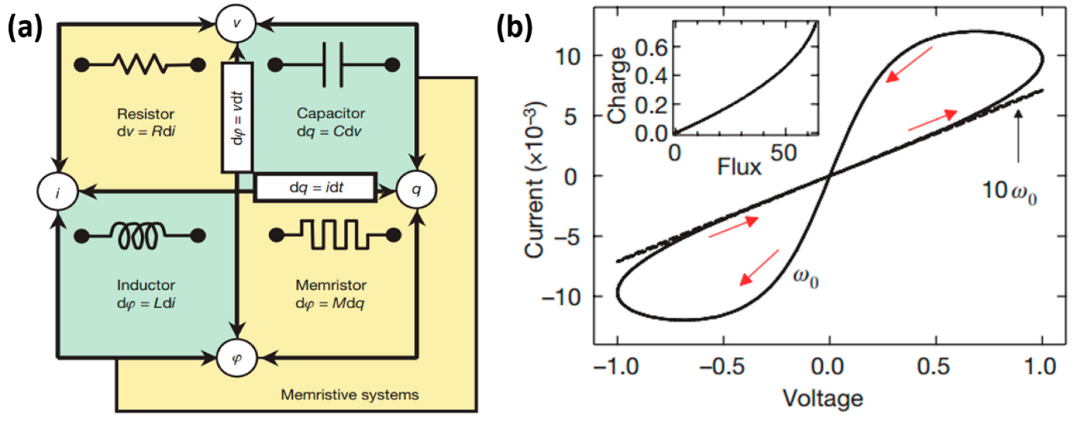
Figure 1.
(a) Theoretical propose of memristor as one of the four fundamental two-terminal circuit elements; (b) physical realization of the memristor through a titanium dioxide device and its electrical characteristics. Reproduced with permission from [2]. Copyright 2008 Springer Nature.
Figure 1.
(a) Theoretical propose of memristor as one of the four fundamental two-terminal circuit elements; (b) physical realization of the memristor through a titanium dioxide device and its electrical characteristics. Reproduced with permission from [2]. Copyright 2008 Springer Nature.

Figure 2.
Schematic illustration of active electrode ion evolution during resistive switching process in electrochemical metallization (ECM) device. Reproduced with permission from [28]. Copyright 2017 John Wiley & Sons, Inc.
Figure 2.
Schematic illustration of active electrode ion evolution during resistive switching process in electrochemical metallization (ECM) device. Reproduced with permission from [28]. Copyright 2017 John Wiley & Sons, Inc.

Figure 3.
(a) Cyclic voltammetry of a Cu/SiO2/Pt device with positive and negative current density peaks corresponding to oxidation and reduction processes of Cu ions, respectively. Reproduced with permission from [29]. Copyright 2017 Royal Society of Chemistry. (b) Current density peak value versus the voltage sweeping rate. Reproduced with permission from [30]. Copyright 2011 AIP Publishing.

Figure 4.
Scanning tunneling microscope (STM) images of RbAg4I5 surface (a) before applying a voltage pulse and (b) after the Ag cluster being formed; (c) detecting the smallest Ag nanofilament. Reproduced with permission from [31]. Copyright 2012 Springer Nature. (d–g) Nanofilament growth dynamics in different kinetic parameters; (h–l) transition between different nanofilament growth dynamics. Reproduced with permission from [33]. Copyright 2014 Springer Nature.
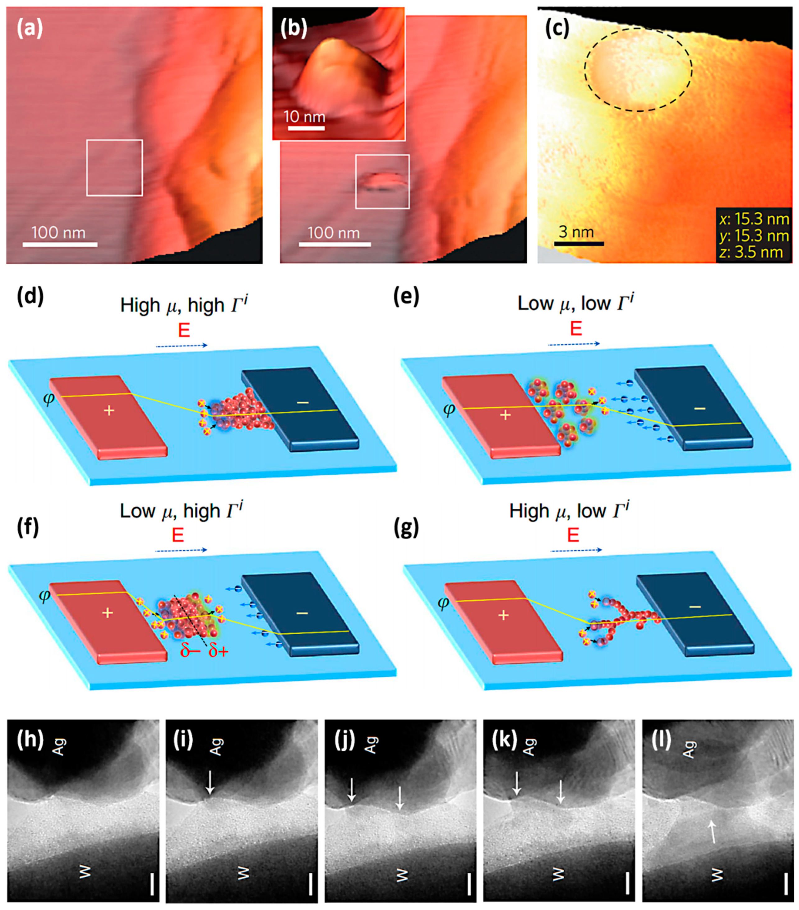
Figure 5.
(a) Schematic illustration of native oxygen ion evolution during resistive switching process in valence change memory (VCM) devices. Reproduced with permission from [28]. Copyright 2017 John Wiley & Sons, Inc. In-situ TEM and HRTEM images of (b,c) the formed and (d,e) ruptured filaments in Pt/ZnO/Pt device. The zinc (Zn) conductive filaments formed after Forming and the conductive filaments converted back to ZnO1−x after Reset. Reproduced with permission from [43]. Copyright 2013 American Chemical Society. The Reset induced (f) Ti4O7 Magnéli structure disappearing and transforming to (g) TiO2 phase in Pt/TiO2/Pt cell. Reproduced with permission from [44]. Copyright 2010 Springer Nature. (h) The VO2 nanochannel formed in the fully electroformed Pt/V2O5/Pt device. Reproduced with permission from [45]. Copyright 2017 John Wiley & Sons, Inc.
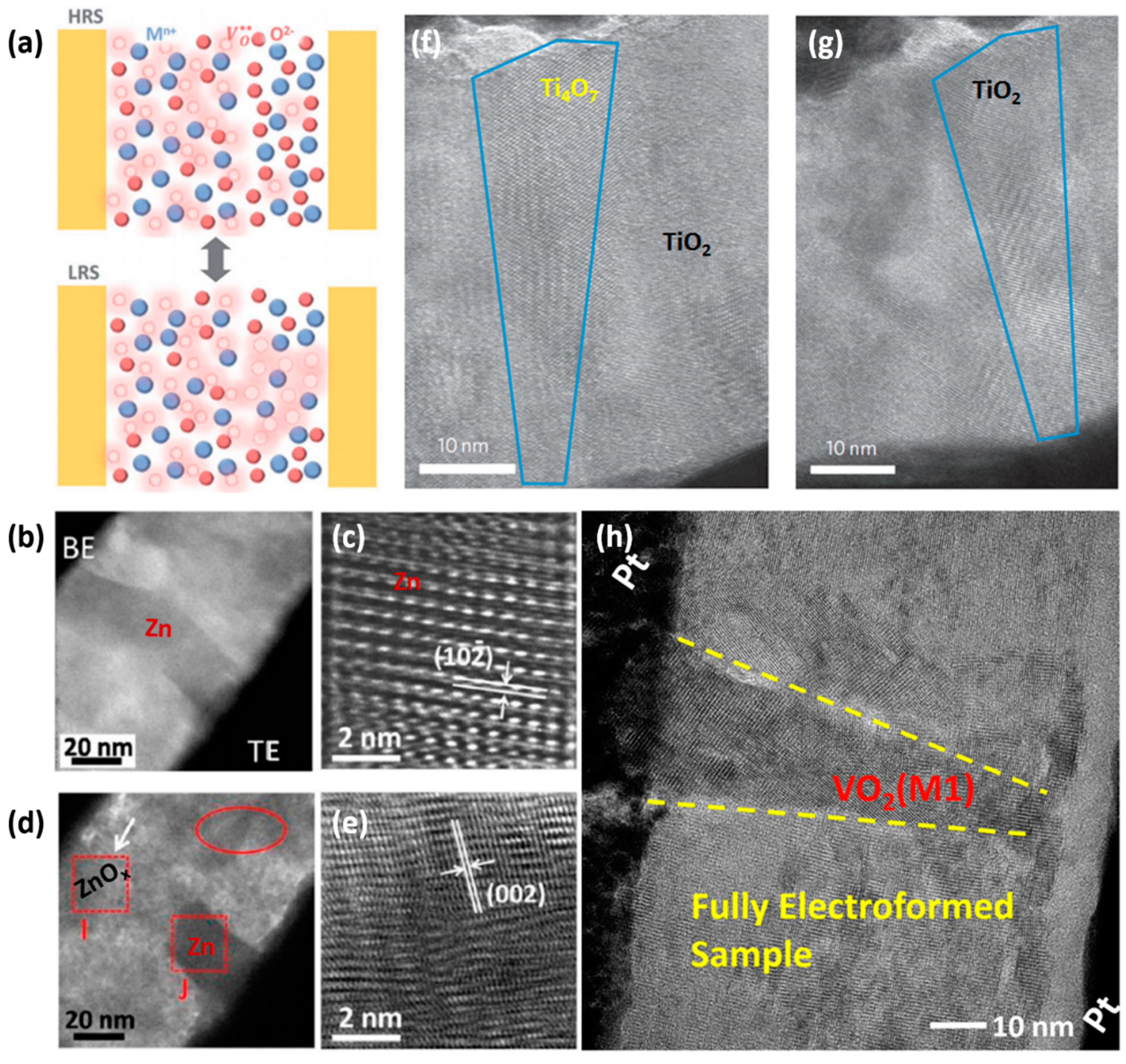
Figure 6.
Detection of native oxygen migration. (a) Electron holography images of the TiN/HfOx/AlOy/Pt device before Forming, after Forming and Reset; (b) the low-energy-filtered images at the low resistance state showing oxygen concentration reducing. Reproduced with permission from [48]. Copyright 2017 John Wiley & Sons, Inc. (c) Topographic of the HfO2/TiN sample showing positions of applied different bias; (d) 1ω and (e) 2ω results of corresponding to (c) through electrostatic force microscopy (EFM) measurement; (f) schematic illustration of formation and dissolution processes of oxygen-deficient nanofilament by electric field induced oxygen ions moving in VCM device. Reproduced under the terms of the Creative Commons Attribution 4.0 International License from [47] Copyright 2017 the authors.
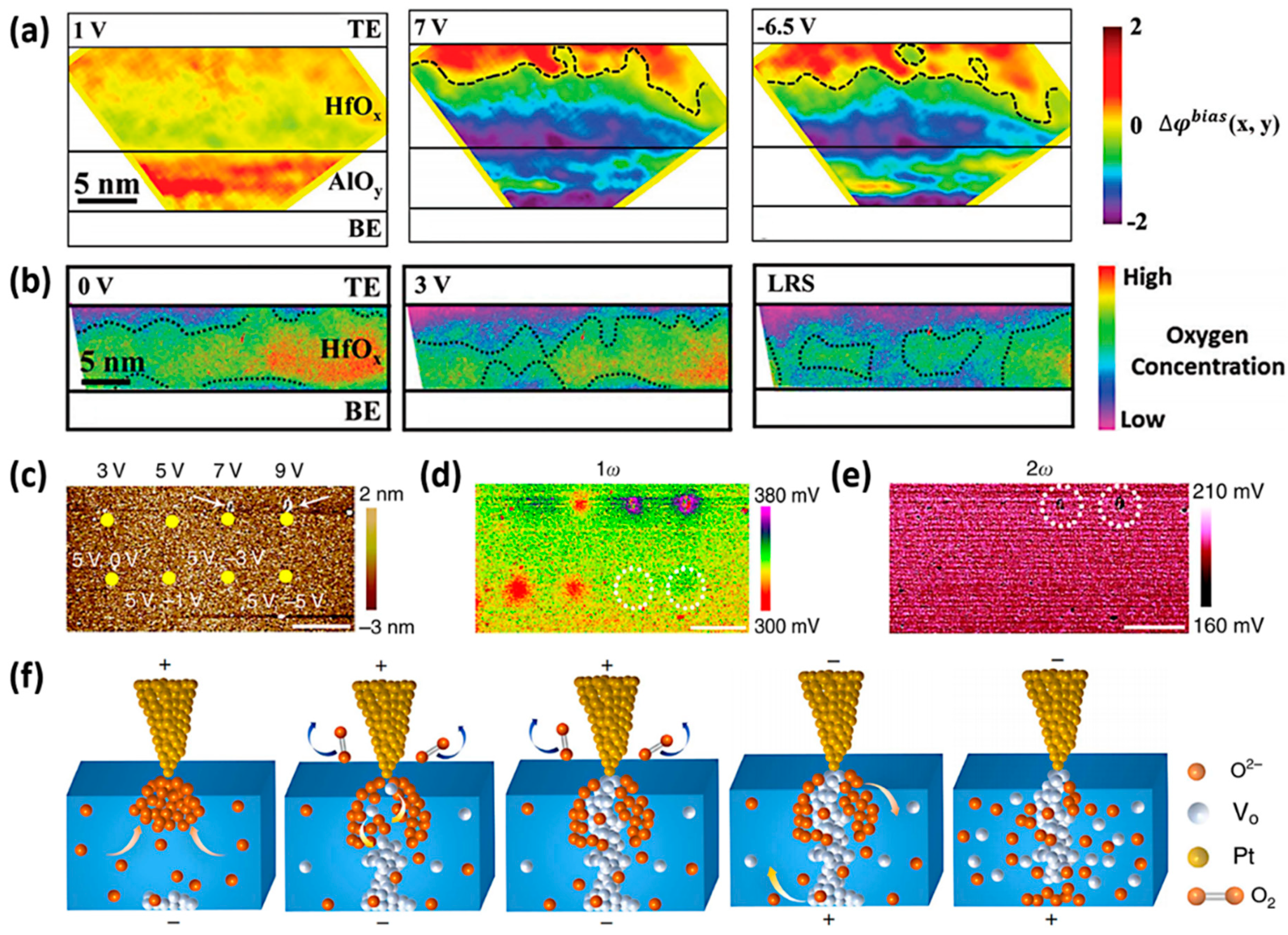
Figure 7.
(a) Conductive atomic force microscopy (C-AFM) images of LixCoO2 film under various voltage biases indicating Li ions preferentially migrating at the grain boundary; (b) morphology of a LixCoO2 grain and (c) threshold forming voltages at different positions away from the grain boundaries in the same nanocrystal; (d) location dependence of the threshold voltage. Reproduced under the terms of the Creative Commons Attribution 3.0 International License from [49] Copyright 2013 the authors. (f) EDX analysis of I elemental distributions at locations 1–4 (e) in electroformed Ag/ CH3NH3PbI3 (MAPbI3)/Ag devices; (g) I/Pb concentration ratio at four locations in the pristine, low resistance and high resistance states; (h) schematics of I ions moving and VI conductive channel forming. Reproduced with permission from [50]. Copyright 2017 John Wiley & Sons, Inc.

Figure 8.
(a) Injection of Li ion into the α-MoO3 channel by positive gate voltage and (b) extraction of Li ion back to the electrolyte by negative gate voltage. Reproduced with permission from [56]. Copyright 2018 John Wiley & Sons, Inc. high resolution TEM (HRTEM) observations of the WSe2 channel under (c,d) 60 and (f,g) 7500 gate pulses, showing that larger numbers of the applied gate pulses can lead to more significant structural disorders. Schematic illustrations of (e) Li+ adsorption on the surface of the WSe2 and (h) subsequent Li+ intercalations into the WSe2 layer. Reproduced with permission from [57]. Copyright 2018 John Wiley & Sons, Inc. (i) The formation of an EDL under applying a lower positive VG (VG < VT) and (j) H+ ions intercalation from aqueous solution into WO3 film with a larger positive VG (VG > VT). Reproduced with permission from [61]. Copyright 2018 John Wiley & Sons, Inc.
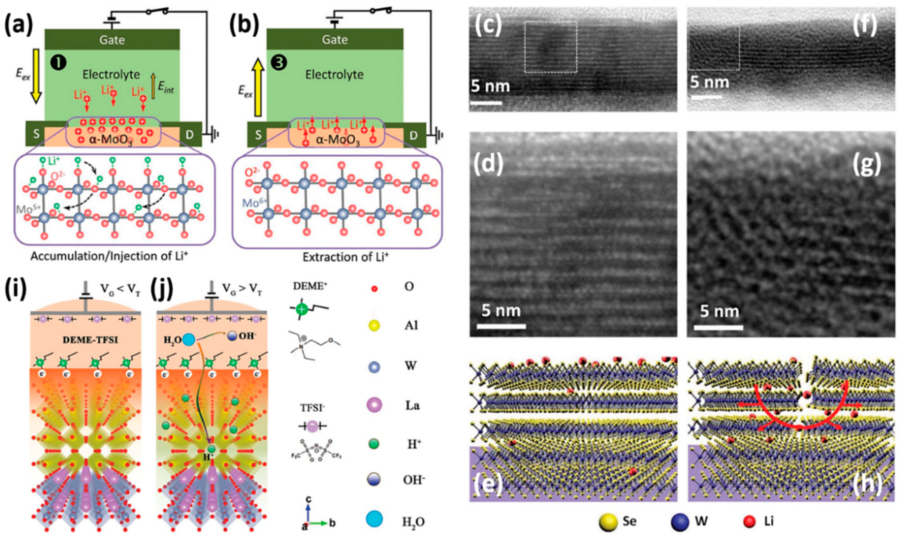
Figure 9.
(a) Schematic illustration and I-V properties of the PQT/[EV(ClO4)2]-based device; (b) Raman images of the device under different voltage biases. Reproduced with permission from [76]. Copyright 2012 American Chemical Society. (c) Molecular structure of pendants of triphenylamine (TPA) and ferrocene (Fc) (PFTPA-Fc); (d) fluorescence line scans of PFTPA-Fc-based devices (d) in the initial state, (e) under applied smaller voltage (2 V) and (f) under applied higher voltage (5 V). Reproduced under the terms of the Creative Commons Attribution 4.0 International License from [77] Copyright 2019 the authors.

Figure 10.
(a) OFF/ON ratios and (b) Set/Reset switching voltages of ZnO-based devices with various electrodes. Reproduced with permission from [78]. Copyright 2014 IOP Publishing. (c) Schematic illustration of resistive switching in the Ag pyramid modified Ag/Al2O3/Pt memristive device; (d) distribution of the electric field near the tip in the pyramid structure. Reproduced with permission from [84]. Copyright 2016 John Wiley & Sons, Inc. (e) Cross sectional TEM images of electroformed device implanted by the Au NPs with incomplete nanofilaments. Reproduced with permission from [85]. Copyright 2016 John Wiley & Sons, Inc.
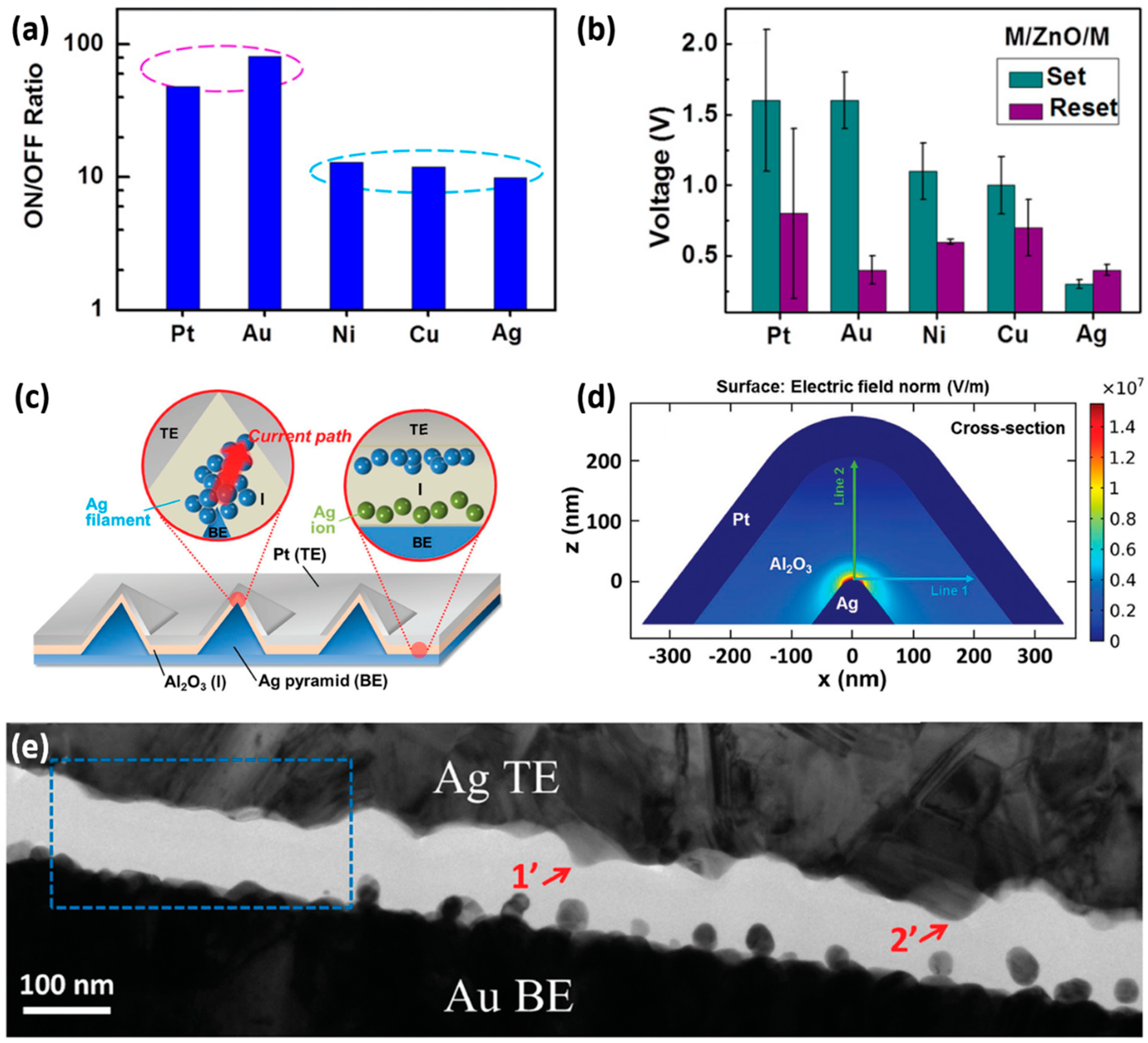
Figure 11.
(a) The native oxygen ions moving induced resistive switching in the Pt/Ta2O5−x/TaO2−x/Pt memristive device; (b) HRTEM images of the (top left) uncycled and (top right) cycled samples; metal Ta clusters were found in the cycled sample by energy-filtered; (c) XPS depth profiles of the A (Ta2O5−x) and B (TaO2−x) regions. Reproduced with permission from [89]. Copyright 2011 Springer Nature. (d) HRTEM image of the Ta/multilayer graphene/Ta2O5/Pd device; the inset shows formation of controllable oxygen vacancies nanofilament in the graphene-inserted device by oxygen ions passing only a nanopore created in the graphene; (e) tuning of the I−V characteristics by the size of nanopores fabricated in the graphene. Reproduced with permission from [91]. Copyright 2016 American Chemical Society. TEM images of electroformed (f) Pt/Ta2O5/Pt and (g) Ta/Ta2O5/Pt samples where cone-shaped nanofilament formed in the Ta-based device with uniform memristive performance. Reproduced with permission from [90]. Copyright 2018 American Chemical Society. (h) Forming voltages dependence on roughness of ZnO deposited on various electrodes. Reproduced with permission from [78]. Copyright 2014 IOP Publishing.

Figure 12.
(a) The setup of isotope labeling measurements in the Pt/SrTiO3/Nb:SrTiO3 device with N2/H218O atmosphere; (b) Secondary-ion mass spectrometry of 18O− depth profile in the different cycled SrTiO3 samples. Endurance performances of memristive devices in (c) humid N2 and (d) dry N2 atmospheres. Reproduced with permission from [27]. Copyright 2018 John Wiley & Sons, Inc.
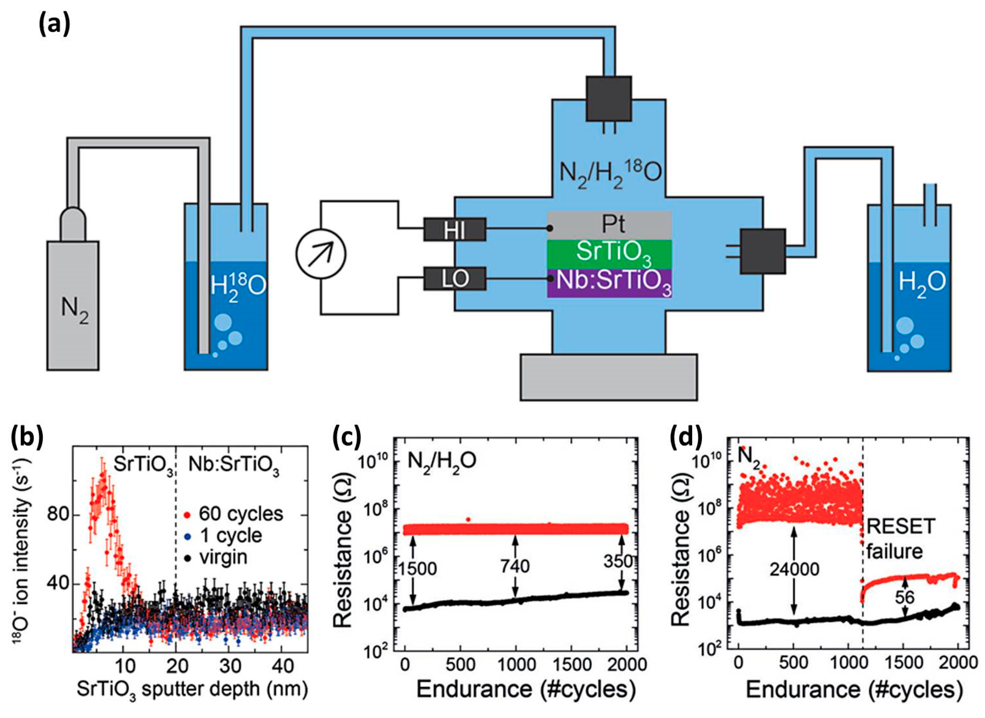
Figure 13.
(a) Phase diagram of a metal-oxygen (Me-O) system with high endurance and repeatability. Reproduced with permission from [100]. Copyright 2013 Springer Nature. (b) The forming voltages of the memristive device (Cu/Ta2O5/Pt) with different Ta2O5 film densities and (c) the effect of Ta2O5 film density on the Cu ions evolution. Reproduced with permission from [106]. Copyright 2015 John Wiley & Sons, Inc. (d) Schematic illustration of self-assembled Sm-doped CeO2 (SDC): SrTiO3 (STO) oxide films and the electric measurement setup; (e) uniform memristive cycles (over 103) in the self-assembled film-based device. Reproduced with permission from [107]. Copyright 2016 Springer Nature. (f) Schematic illustration of the formation of nanofilaments in the amorphous-nanocrystalline HfOx films and (g) endurance performance of the device. Reproduced with permission from [109]. Copyright 2014 Royal Society of Chemistry.

© 2019 by the authors. Licensee MDPI, Basel, Switzerland. This article is an open access article distributed under the terms and conditions of the Creative Commons Attribution (CC BY) license (http://creativecommons.org/licenses/by/4.0/).
Share and Cite
MDPI and ACS Style
Xue, W.; Xu, X.-H.; Liu, G. Solid-State Electrochemical Process and Performance Optimization of Memristive Materials and Devices. Chemistry 2019, 1, 44-68. https://doi.org/10.3390/chemistry1010005
AMA Style
Xue W, Xu X-H, Liu G. Solid-State Electrochemical Process and Performance Optimization of Memristive Materials and Devices. Chemistry. 2019; 1(1):44-68. https://doi.org/10.3390/chemistry1010005
Chicago/Turabian StyleXue, Wuhong, Xiao-Hong Xu, and Gang Liu. 2019. "Solid-State Electrochemical Process and Performance Optimization of Memristive Materials and Devices" Chemistry 1, no. 1: 44-68. https://doi.org/10.3390/chemistry1010005