A Soft-Switched DC/DC Converter Using Integrated Dual Half-Bridge with High Voltage Gain and Low Voltage Stress for DC Microgrid Applications


Abstract
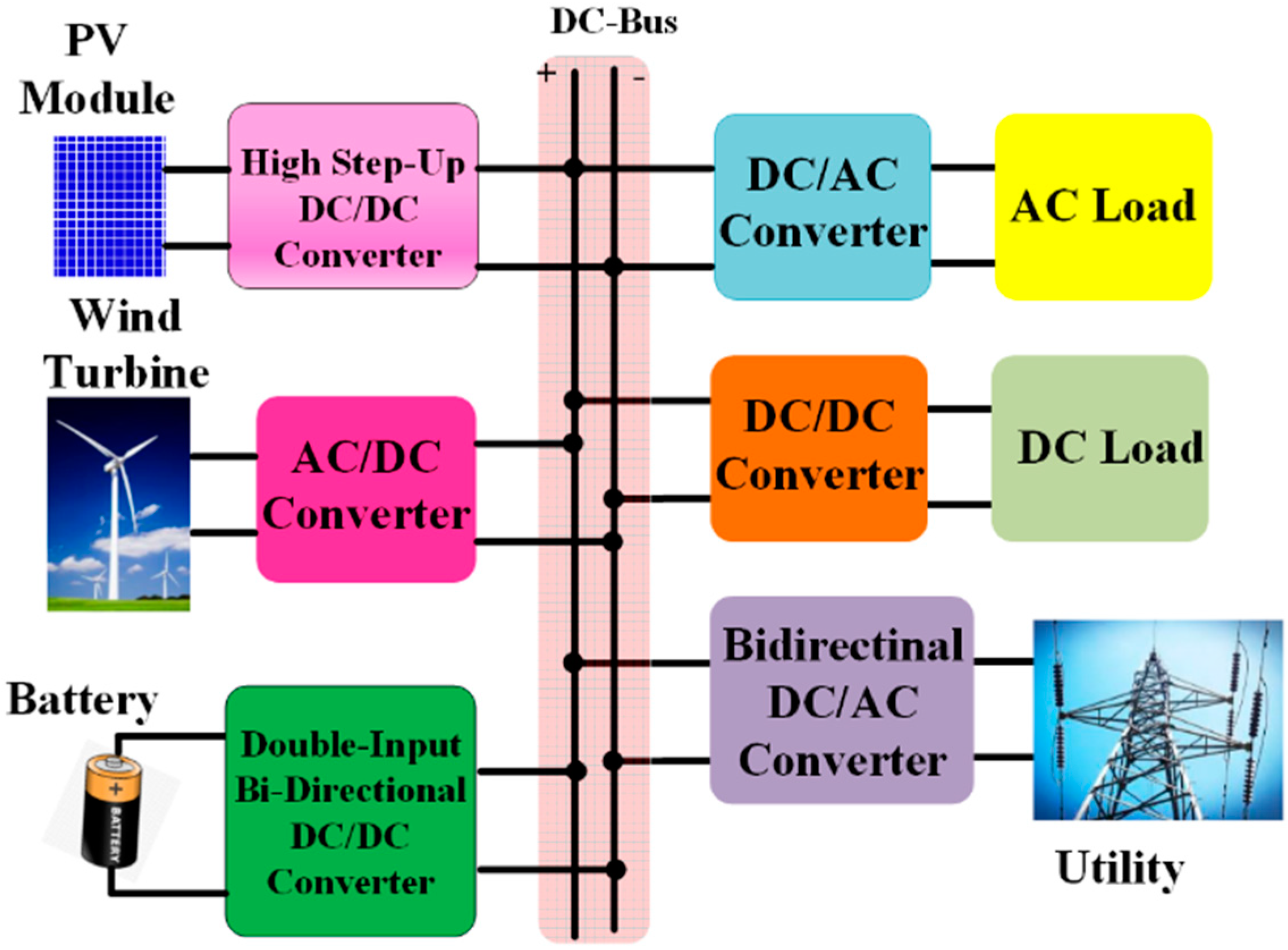
:1. Introduction
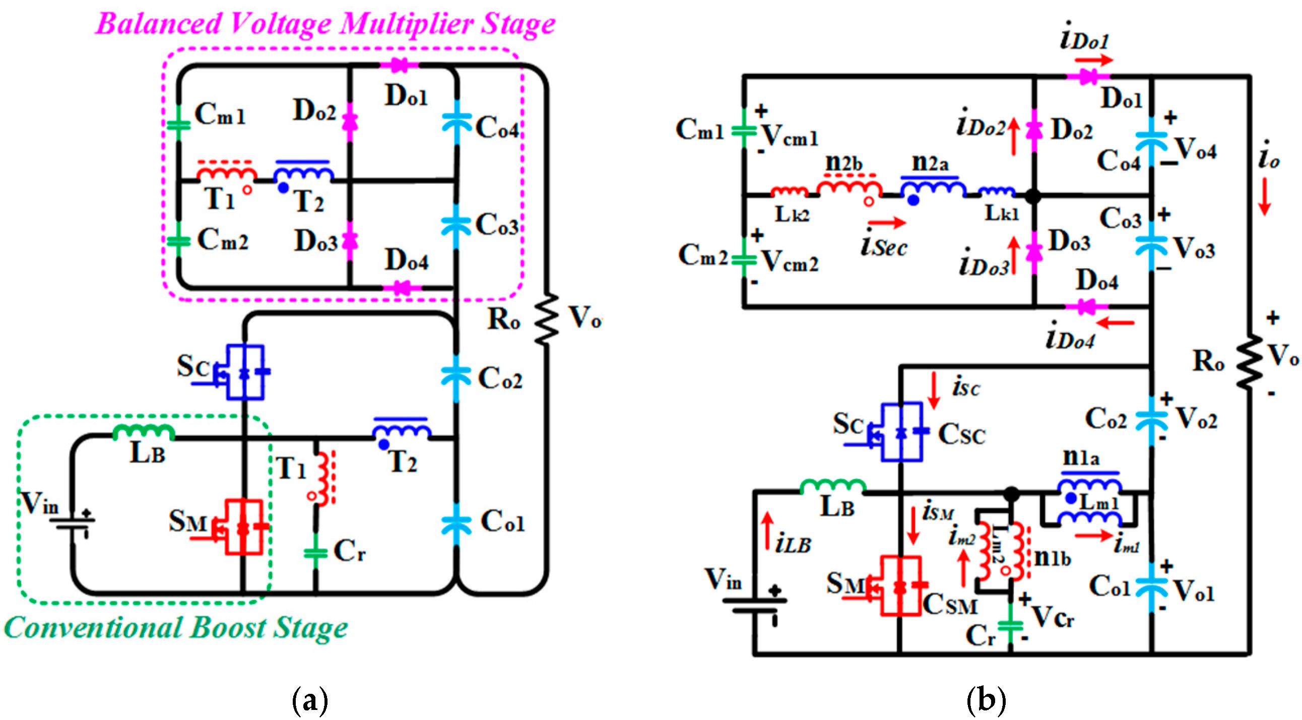
2. Structure and Operating Principles of the Proposed Converter
2.1. General Structure
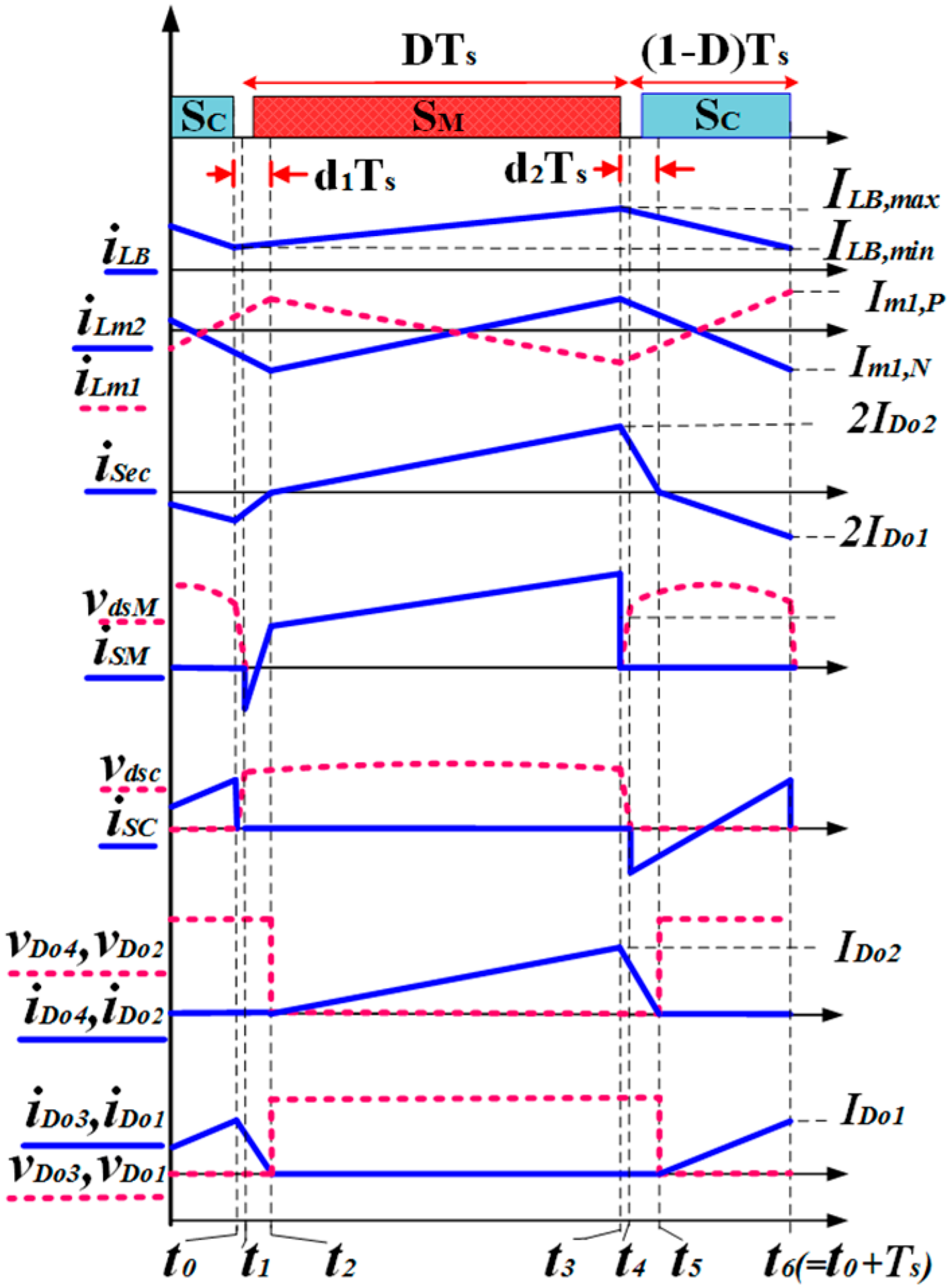
2.2. Operation Modes
- (1)
- The inductor Lk shows the total inductance of leakage inductors Lk1 and Lk2.
- (2)
- all passive and active semiconductors are considered ideal; and
- (3)
- the capacitors are large enough to assume that their voltage is constant during one switching period.
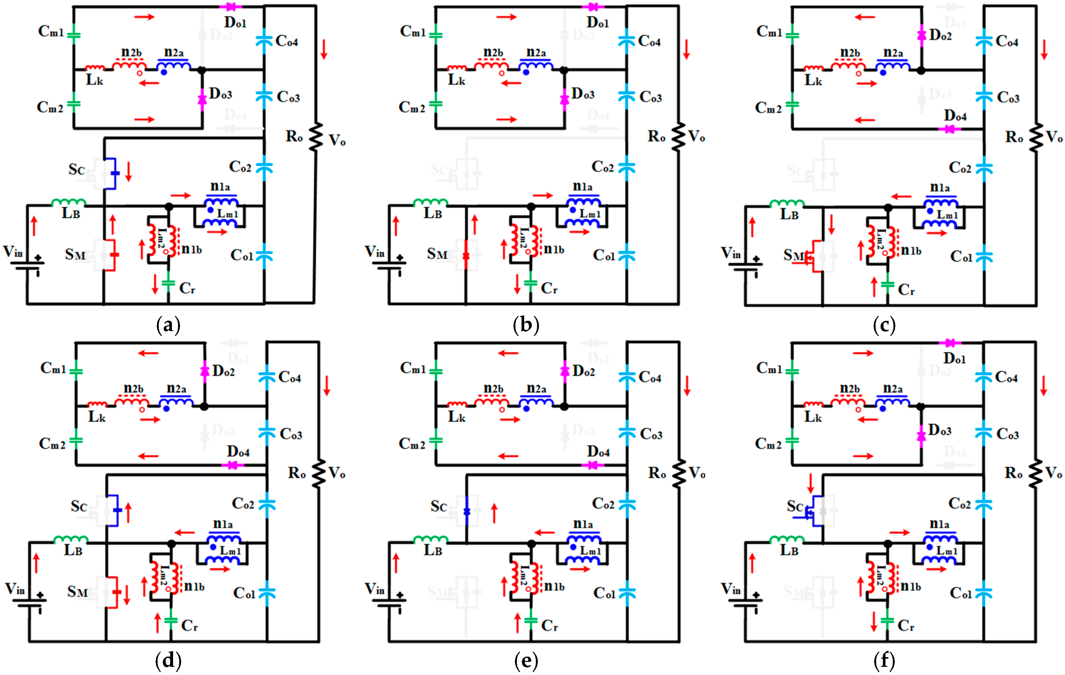
2.2.1. Mode 1 [t0–t1]
2.2.2. Mode 2 [t1–t2]
2.2.3. Mode 3 [t2–t3]
2.2.4. Mode 4 [t3–t4]
2.2.5. Mode 5 [t4–t5]
2.2.6. Mode 6 [t5–t6]
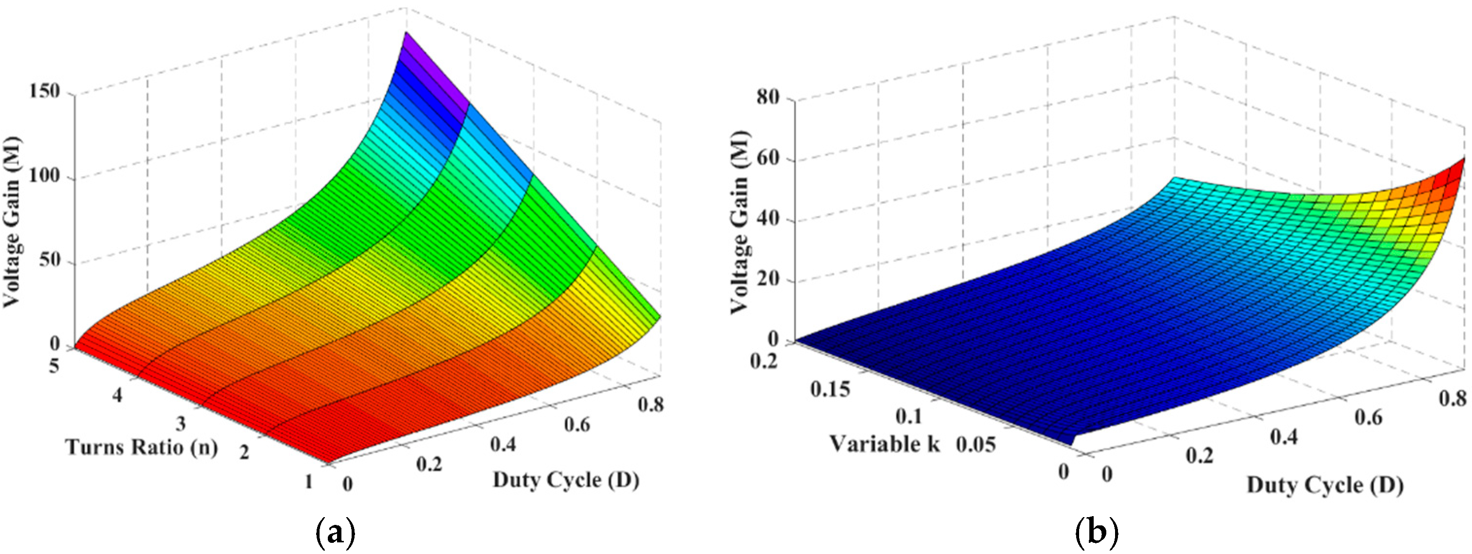
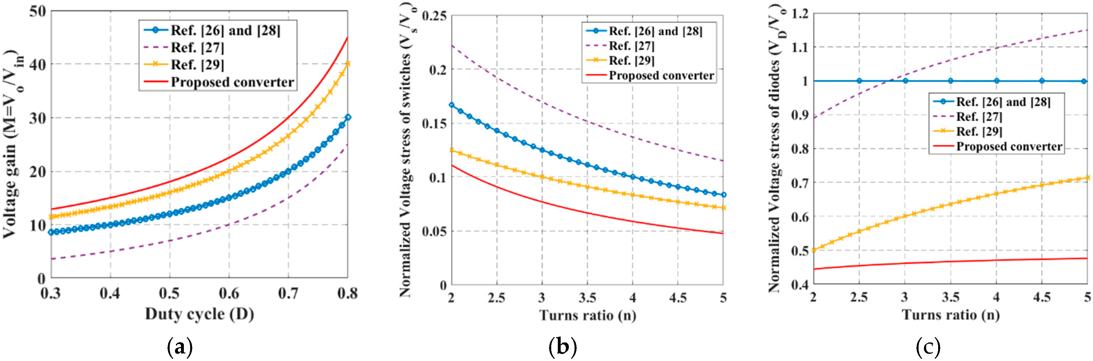
2.3. Voltage Gain
2.4. Voltage Stress Across Switches and Diodes
2.5. The Magnetizing Inductor Minimum and Maximum Currents im1 and im2
2.6. ZVS Soft-Switching Conditions for Switches SM and SC
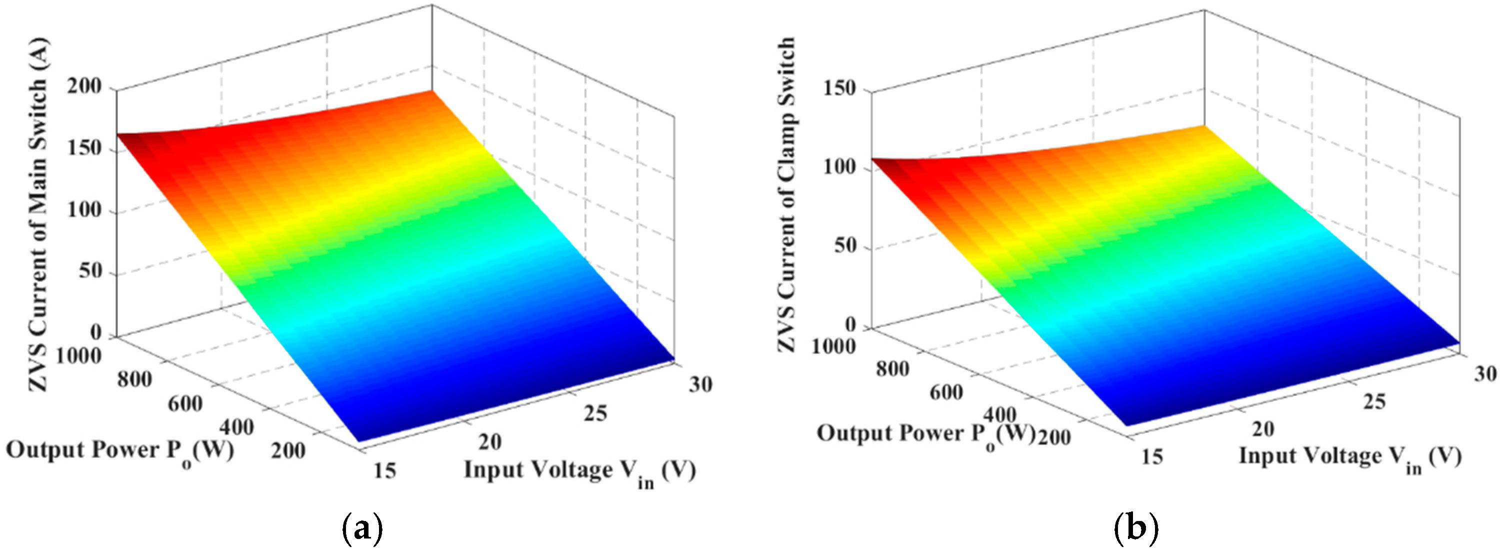
2.7. Current Stress of Power Switches and Diodes
2.8. Comparison with Other High Step-Up Converters
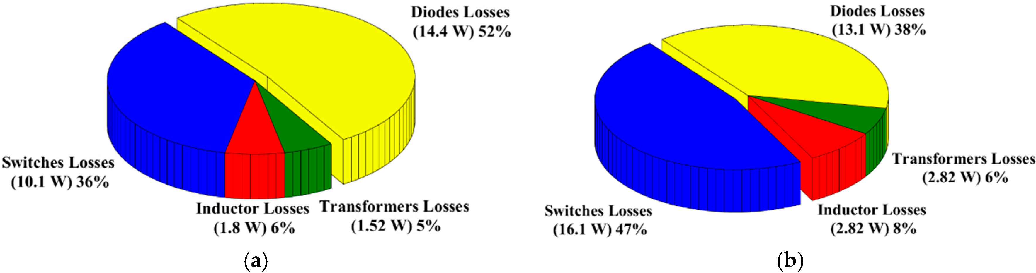
2.9. Loss Analysis of Proposed Converter
2.9.1. Conduction Loss of Switches
2.9.2. Switching Loss of Transistors
2.9.3. Diode Losses
2.9.4. Inductor Losses
2.9.5. Transformer Losses
3. Design Considerations
3.1. Selection of Turns Ratio
3.2. Choice of Leakage Inductance
3.3. Choice of Magnetizing Inductance
3.4. Choice of Boost Inductance
3.5. Design of Capacitors
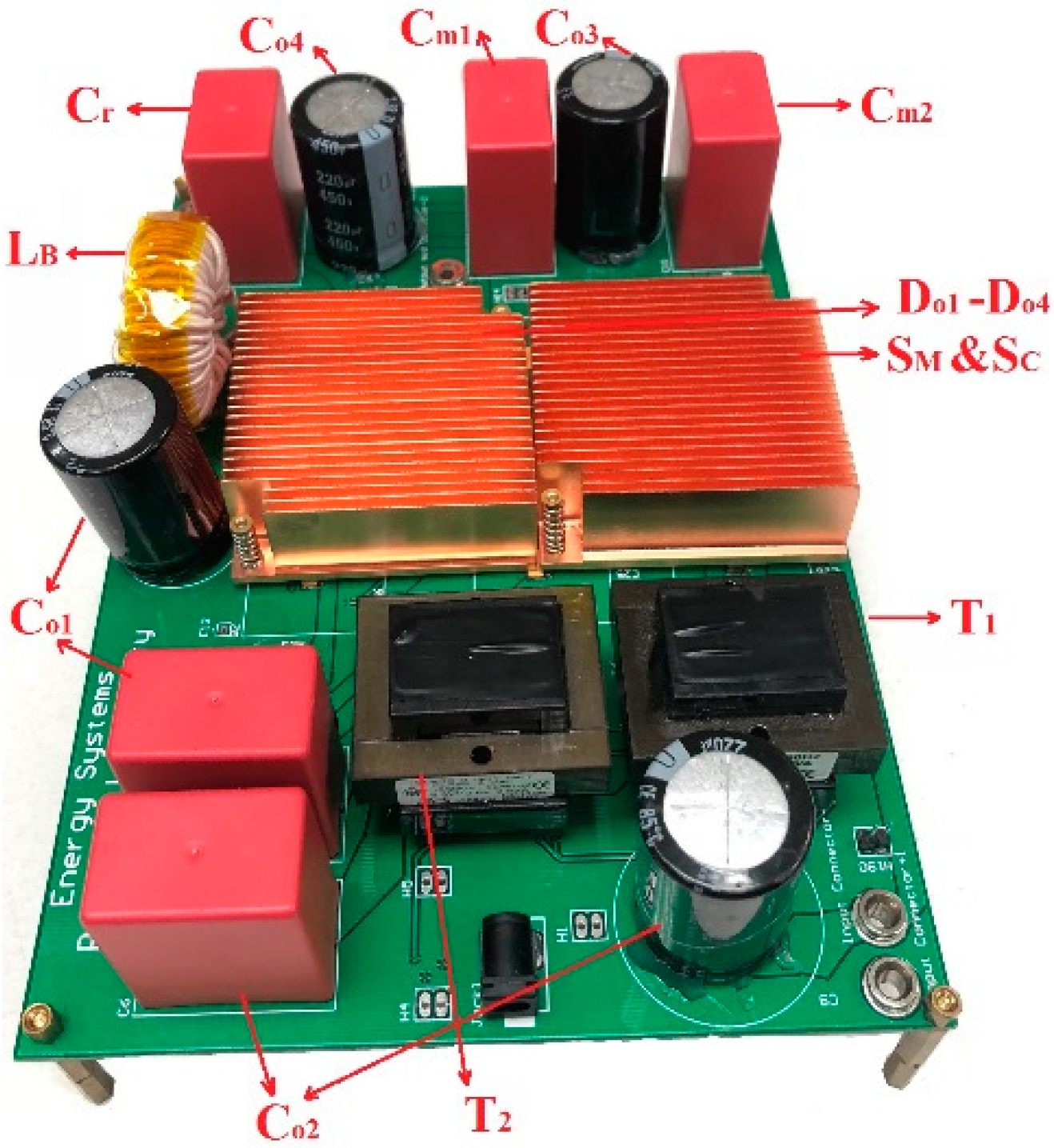
4. Simulation and Experimental Results
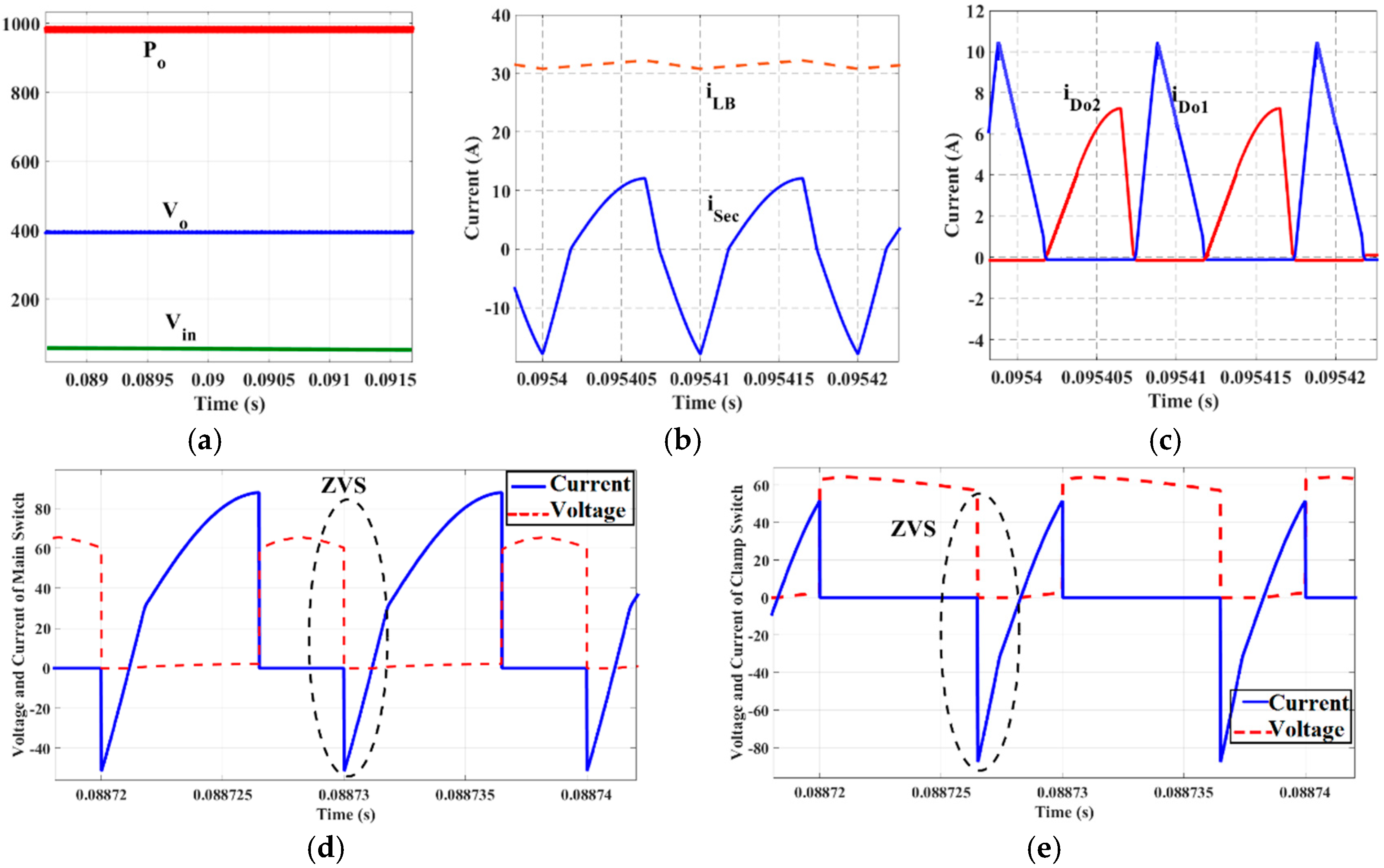
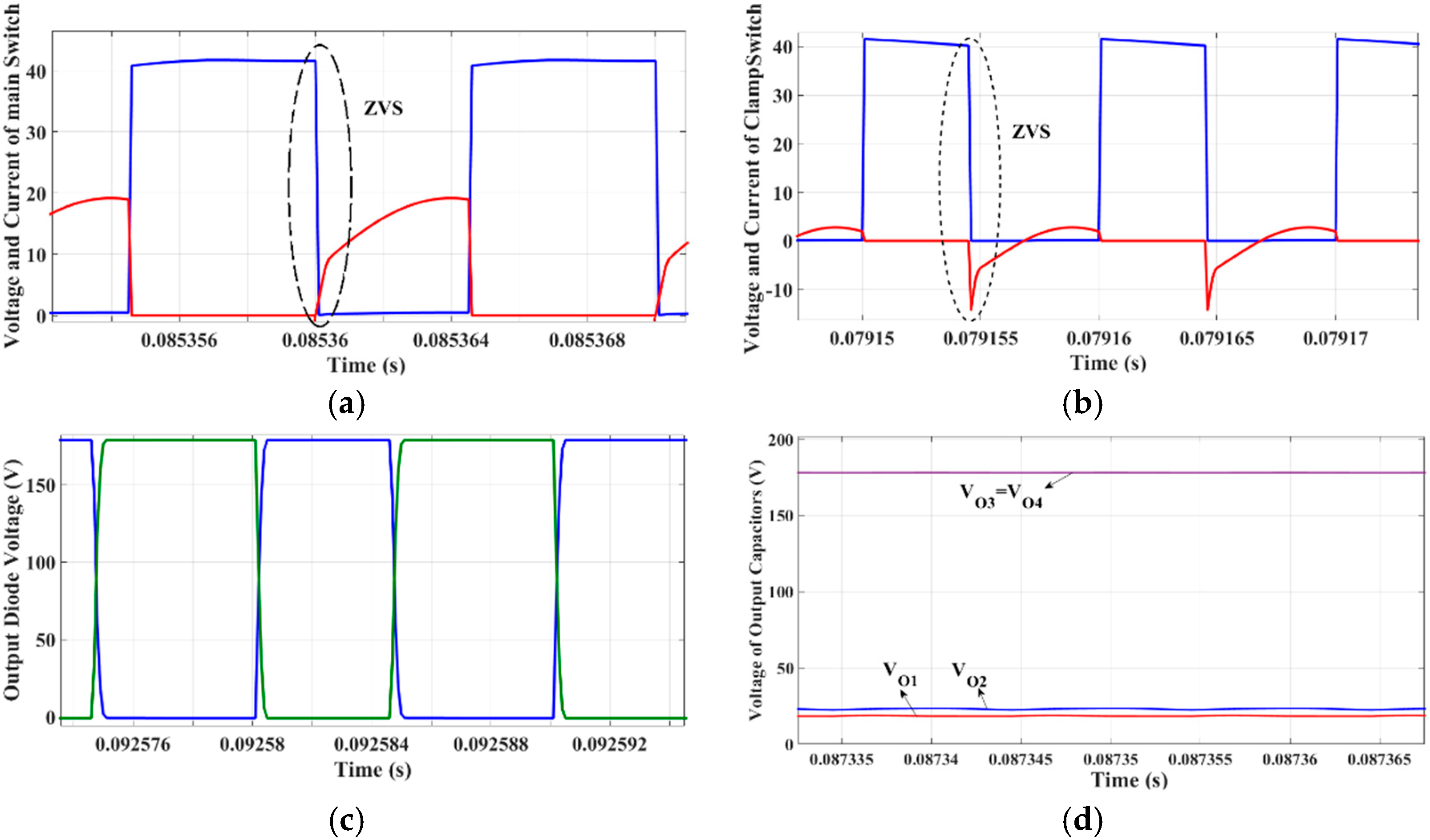
4.1. Simulation Results
4.1.1. Full Load Condition (Vin = 22 V, Po = 1000 W, and D = 0.65)
4.1.2. Light Load condition (Vin = 22 V, Po = 100 W, and D = 0.48)
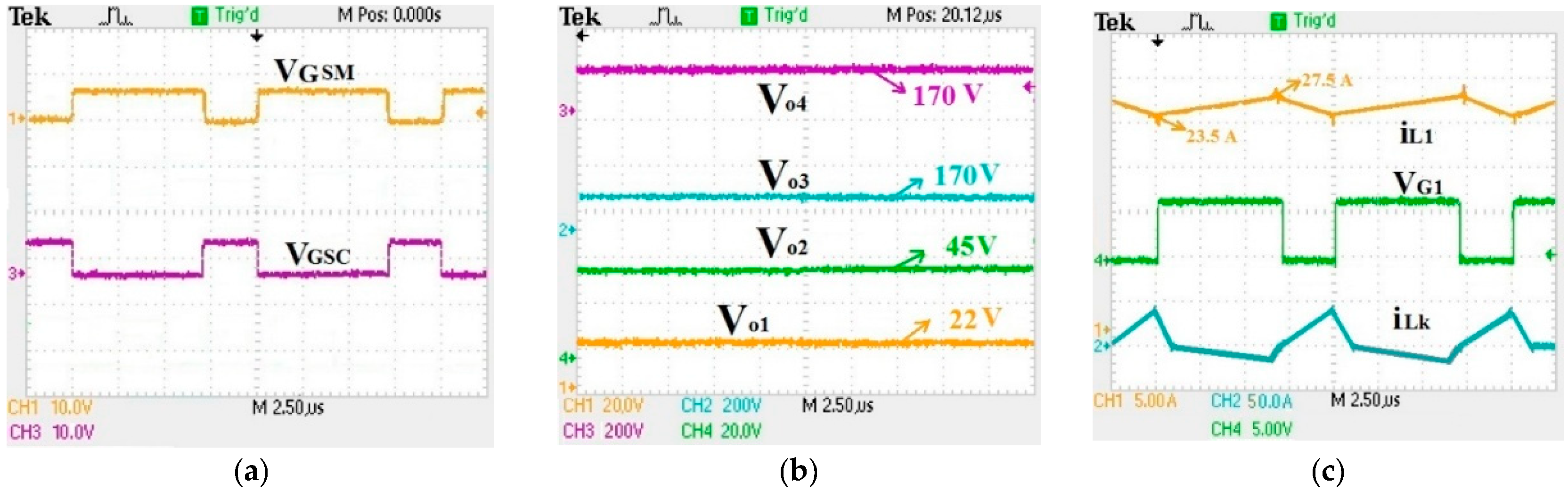
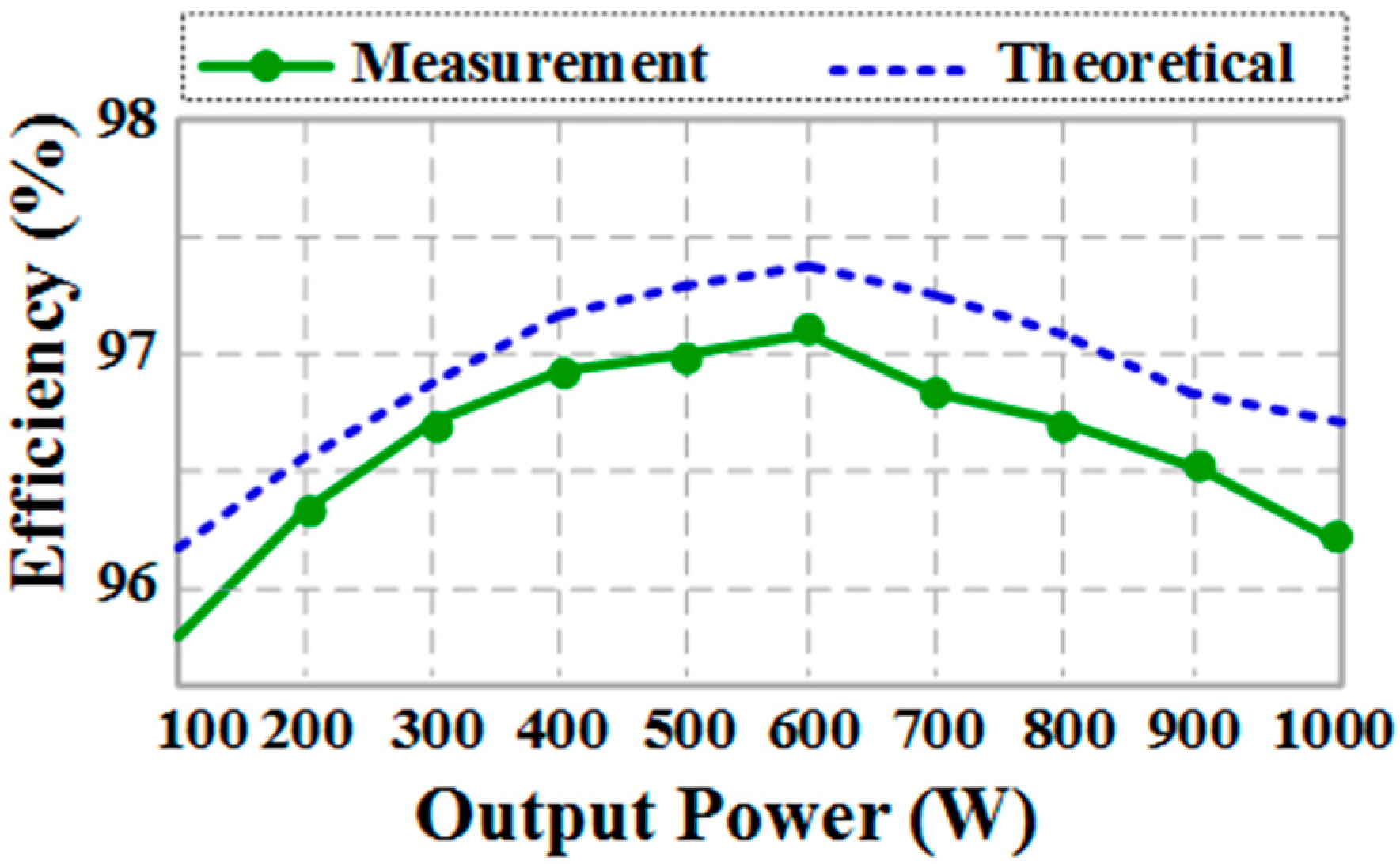
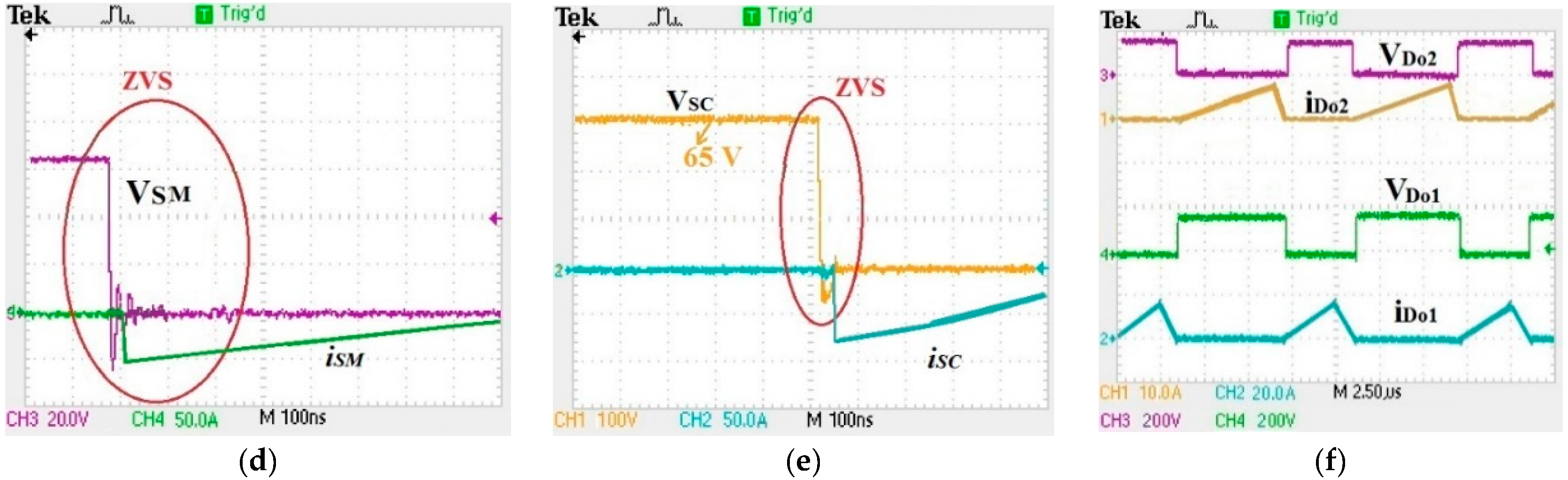
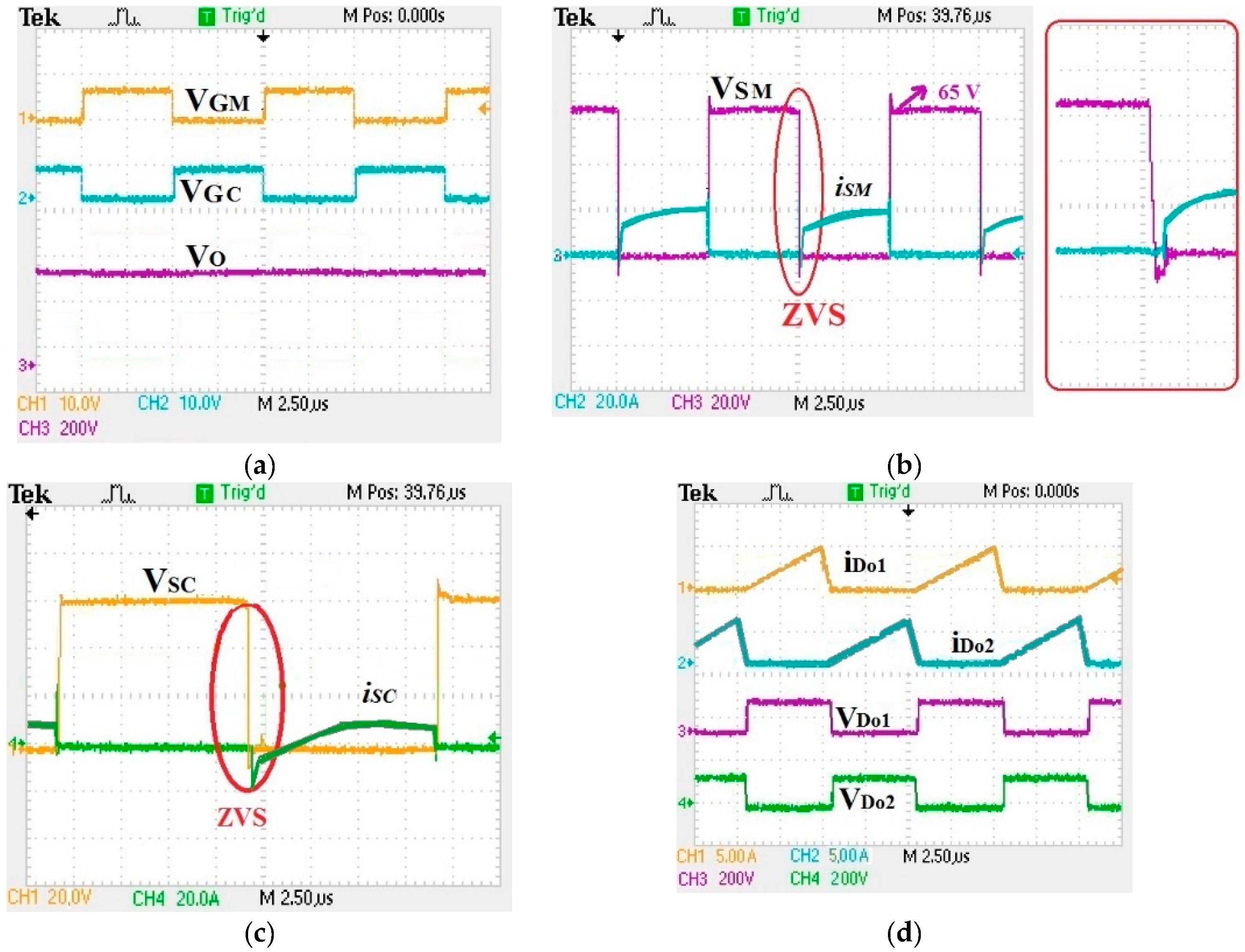
4.2. Experimental Results
5. Conclusions
Author Contributions
Funding
Conflicts of Interest
References
- Chirapongsananurak, P.; Santoso, S. Inventions and Innovation in Integration of Renewable Energy Systems. Inventions 2018, 3, 28. [Google Scholar] [CrossRef]
- Sathyan, S.; Suryawanshi, H.M.; Shitole, A.B.; Ballal, M.S.; Borghate, V.B. Soft-Switched Interleaved DC/DC Converter as Front-End of Multi-Inverter Structure for Micro Grid Applications. IEEE Trans. Power Electron. 2018, 33, 7645–7655. [Google Scholar] [CrossRef]
- Pilz, M.; Al-Fagih, L.; Pfluegel, E.I. Energy Storage Scheduling with an Advanced Battery Model: A Game–Theoretic Approach. Inventions 2017, 2, 30. [Google Scholar] [CrossRef]
- Ebrahim, A.F.; Mohammed, O.A. Pre-Processing of Energy Demand Disaggregation Based Data Mining Techniques for Household Load Demand Forecasting. Inventions 2018, 3, 45. [Google Scholar] [CrossRef]
- Zhang, Y.; Fu, C.; Sumner, M.; Wang, P. A Wide Input-Voltage Range Quasi-Z-Source Boost DC–DC Converter with High-Voltage Gain for Fuel Cell Vehicles. IEEE Trans. Ind. Electron. 2018, 65, 5201–5212. [Google Scholar] [CrossRef]
- Tseng, K.C.; Cheng, C.A.; Chen, C.T. High Step-Up Interleaved Boost Converter for Distributed Generation Using Renewable and Alternative Power Sources. IEEE J. Emerg. Sel. Top. Power Electron. 2017, 5, 713–722. [Google Scholar] [CrossRef]
- Mira, M.C.; Zhang, Z.; Knott, A.; Andersen, M.A.E. Analysis, Design, Modeling, and Control of an Interleaved-Boost Full-Bridge Three-Port Converter for Hybrid Renewable Energy Systems. IEEE Trans. Power Electron. 2017, 32, 1138–1155. [Google Scholar] [CrossRef]
- Wu, B.; Li, S.; Liu, Y.A. New Hybrid Boosting Converter for Renewable Energy Applications. IEEE Trans. Power Electron. 2016, 31, 1203–1215. [Google Scholar] [CrossRef]
- Zhao, B.; Song, Q.; Liu, W.; Sun, Y. Overview of dual-active bridge isolated bidirectional DC-DC converter for high-frequency-link power-conversion system. IEEE Trans. Power Electron. 2014, 29, 4091–4106. [Google Scholar] [CrossRef]
- Chu, E.; Hou, X.; Zhang, H.; Wu, M.; Liu, X. Novel zero-voltage and zero-current switching (ZVZCS) PWM three-level DC/DC converter using output coupled inductor. IEEE Trans. Power Electron. 2014, 29, 1082–1093. [Google Scholar]
- Tseng, K.C.; Huang, C.C.; Cheng, C.A. A high step-up converter with voltage-multiplier modules for sustainable energy applications. IEEE J. Emerg. Sel. Top. Power Electron. 2015, 3, 1100–1108. [Google Scholar] [CrossRef]
- Baddipadiga, B.P.R.; Prabhala, V.A.; Ferdowsi, M. A Family of High-Voltage-Gain DC-DC Converters Based on a Generalized Structure. IEEE Trans. Power Electron. 2018, 33, 8399–8411. [Google Scholar] [CrossRef]
- Nejad, M.L.; Poorali, B.; Adib, E.; Birjandi, A.A.M. New cascade boost converter with reduced losses. IET Power Electron. 2016, 9, 1213–1219. [Google Scholar] [CrossRef]
- Zhang, Y.; Shi, J.; Zhou, L. Wide Input-Voltage Range Boost Three-Level DC–DC Converter with Quasi-Z Source for Fuel Cell Vehicles. IEEE Trans. Power Electron. 2017, 32, 6728–6738. [Google Scholar] [CrossRef]
- Forouzesh, M.; Siwakoti, Y.P.; Gorji, S.A. Step-Up DC–DC Converters: A Comprehensive Review of Voltage-Boosting Techniques, Topologies, and Applications. IEEE Trans. Power Electron. 2017, 32, 9143–9178. [Google Scholar] [CrossRef]
- Lee, J.H.; Liang, T.J.; Chen, J.F. Isolated coupled-inductor integrated DC-DC converter with nondissipative snubber for solar energy applications. IEEE Trans. Ind. Electron. 2014, 61, 3337–3348. [Google Scholar] [CrossRef]
- Kang, H.; Cha, H. A New Nonisolated High-Voltage-Gain Boost Converter with Inherent Output Voltage Balancing. IEEE Trans. Ind. Electron. 2018, 65, 2189–2198. [Google Scholar] [CrossRef]
- Mousavi, A.; Das, P.; Moschopoulos, G. A comparative study of a new ZCS DC–DC full-bridge boost converter with a ZVS active-clamp converter. IEEE Trans. Power Electron. 2012, 27, 1347–1358. [Google Scholar] [CrossRef]
- Chen, Y.; Huang, A.Q.; Yu, X. A high step-up three-port DC-DC converter for stand-alone PV/battery power systems. IEEE Trans. Power Electron. 2013, 28, 5049–5062. [Google Scholar] [CrossRef]
- Zhao, Q.; Lee, F.C. High-efficiency, high step-up DC-DC converters. IEEE Trans. Power Electron. 2003, 18, 65–73. [Google Scholar] [CrossRef]
- Wai, R.J.; Liaw, J.J. High-efficiency-isolated single-input multiple output bidirectional converter. IEEE Trans. Power Electron. 2015, 30, 4914–4930. [Google Scholar] [CrossRef]
- Shahir, F.M.; Babaei, E.; Farsadi, M. Voltage-Lift Technique Based Non-isolated Boost DC-DC Converter: Analysis and Design. IEEE Trans. Power Electron. 2017, 33, 5917–5926. [Google Scholar] [CrossRef]
- Lai, C.-M. Development of a Novel Bidirectional DC/DC Converter Topology with High Voltage Conversion Ratio for Electric Vehicles and DC-Microgrids. Energies 2016, 9, 410. [Google Scholar] [CrossRef]
- Wang, P.; Zhou, L.; Zhang, Y.; Li, J.; Sumner, M. Input-Parallel Output-Series DC-DC Boost Converter with a Wide Input Voltage Range for Fuel Cell Vehicles. IEEE Trans. Veh. Tech. 2017, 66, 7771–7781. [Google Scholar] [CrossRef]
- Moradisizkoohi, H.; Milimonfared, J.; Taheri, M.; Salehi, S. A high step-up half-bridge DC/DC converter with a special coupled inductor for input current ripple cancelation and extended voltage doubler circuit for power conditioning of fuel cell systems. Int. J. Circuit Theory Appl. 2015, 44, 1290–1307. [Google Scholar] [CrossRef]
- Muhammad, M.; Armstrong, M.; Elgendy, M.A. A Nonisolated Interleaved Boost Converter for High-Voltage Gain Applications. IEEE J. Emerg. Sel. Top. Power Electron. 2016, 4, 352–362. [Google Scholar] [CrossRef]
- Liu, H.; Li, F. A novel high step-up converter with a quasi-active switched-inductor structure for renewable energy systems. IEEE Trans. Power Electron. 2016, 31, 5030–5039. [Google Scholar] [CrossRef]
- Li, W.; Xiang, X.; Li, C.; Li, W.; He, X. Interleaved high step-up ZVT converter with built-in transformer voltage doubler cell for distributed PV generation system. IEEE Trans. Power Electron. 2013, 28, 300–313. [Google Scholar] [CrossRef]
- Chen, S.-J.; Yang, S.-P.; Huang, C.-M.; Chou, H.-M.; Shen, M.-J. Interleaved High Step-Up DC-DC Converter Based on Voltage Multiplier Cell and Voltage-Stacking Techniques for Renewable Energy Applications. Energies 2018, 11, 1632. [Google Scholar] [CrossRef]
- Liu, H.; Zhang, D. Two-phase interleaved inverse-coupled inductor boost without right half plane zeros. IEEE Trans. Power Electron. 2017, 32, 1844–1859. [Google Scholar] [CrossRef]
- Moradi sizkohi, H.; Milimonfared, J.; Taheri, M.; Salehi, S.; Mohammadi, M. Non-isolated high step-up converter based on combination of Flyback and Forward for power conditioning of photovoltaic and fuel-cell systems. In Proceedings of the 6th Power Electronics, Drive Systems & Technologies Conference (PEDSTC2015), Tehran, Iran, 3–4 February 2015; pp. 661–666. [Google Scholar]


| Item | Converter Cited in [26] | Converter Cited in [27] | Converter Cited in [28] | Converter Cited in [29] | Proposed Converter | |
|---|---|---|---|---|---|---|
| Voltage gain | ||||||
| Switch voltage stress | ||||||
| Diode voltage stress | ||||||
| No. of Components | S 1 | 4 | 2 | 4 | 2 | 2 |
| D 2 | 2 | 3 | 4 | 6 | 4 | |
| C 3 | 4 | 3 | 5 | 6 | 7 | |
| L 4 | 0 | 0 | 2 | 0 | 1 | |
| No. of Transformer or coupled inductors | 2 | 2 | 1 | 2 | 2 | |
| Soft-switching | Soft switching (ZVS) | Hard switching | Soft switching (ZVS) | Hard switching | Soft switching (ZVS) | |
| Control circuit | Complex | Simple | Complex | Simple | Simple | |
| Parameter | Value |
|---|---|
| Input DC-voltage (Vin) | 15–30 V |
| Output voltage (Vo) | 400 V |
| Output power (Po) | 1000 W |
| Switching frequency (fs) | 100 kHz |
| Magnetizing inductance (Lm1 and Lm2) | 100 µH |
| Leakage inductance (Lk1 and Lk2) | 10 µH |
| Turns ratio of coupled inductors (n) | 1.5 |
| Switches | EPC2047 (200 V, 160 A, 10 mΩ) |
| Diodes | C3D10065E |
| Output capacitors (Co1, Co2, Co3, and Co4) | 47 µF |
| Switched capacitors (Cm1 and Cm2) | 10 µF |
© 2018 by the authors. Licensee MDPI, Basel, Switzerland. This article is an open access article distributed under the terms and conditions of the Creative Commons Attribution (CC BY) license (http://creativecommons.org/licenses/by/4.0/).
Share and Cite
Moradisizkoohi, H.; Elsayad, N.; Mohammed, O. A Soft-Switched DC/DC Converter Using Integrated Dual Half-Bridge with High Voltage Gain and Low Voltage Stress for DC Microgrid Applications. Inventions 2018, 3, 63. https://doi.org/10.3390/inventions3030063
Moradisizkoohi H, Elsayad N, Mohammed O. A Soft-Switched DC/DC Converter Using Integrated Dual Half-Bridge with High Voltage Gain and Low Voltage Stress for DC Microgrid Applications. Inventions. 2018; 3(3):63. https://doi.org/10.3390/inventions3030063
Chicago/Turabian StyleMoradisizkoohi, Hadi, Nour Elsayad, and Osama Mohammed. 2018. "A Soft-Switched DC/DC Converter Using Integrated Dual Half-Bridge with High Voltage Gain and Low Voltage Stress for DC Microgrid Applications" Inventions 3, no. 3: 63. https://doi.org/10.3390/inventions3030063