1. Introduction
There is a growing global interest in reducing greenhouse gases by developing new clean energy technologies that address the challenges associated with the increasing penetration of renewable energy systems and the need to reduce fossil fuel consumption. The increasing number of automobiles worldwide is a growing problem, because they contribute to air pollution. A lot of research and development is being targeted to develop new fully electric vehicles (EVs) powered by clean energies. Fuel cell-powered EVs are a big contributor to the electrification of automobiles. Fuel cells, as a source of electrical energy, have the following features: pollution-free operation, high-density current output, and high efficiency [
1]. The fuel cell has a low output voltage, which requires a step-up dc–dc converter with a high-voltage gain to solve the voltage mismatch between the fuel cell and the dc-link bus of the three-phase inverter inside a car [
2,
3,
4,
5,
6,
7,
8,
9]. Fuel cells are unlike batteries, as they have soft output characteristics, in that their output voltage drops drastically when the output current increases [
2]. The architecture of a fuel cell-powered EV with a step-up converter is shown in
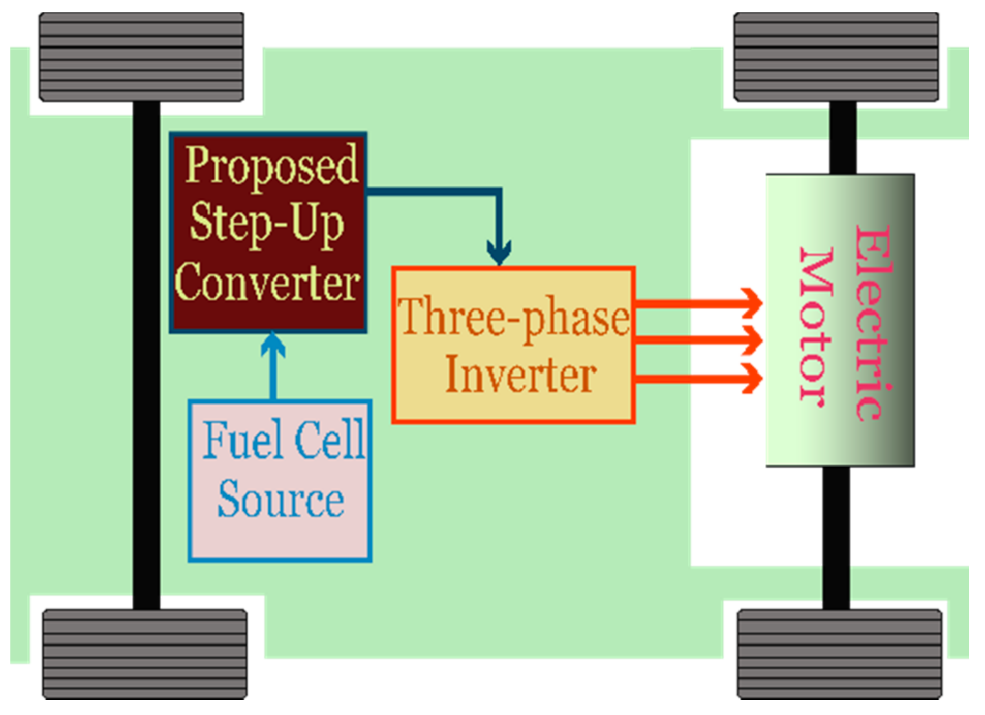
Figure 1. This converter steps up the voltage of the fuel cell to the level required by the three-phase inverter, and the inverter drives the electric motor. The step-up converter should have the following features: wide voltage gain range, high efficiency, small size, low weight, and low input current ripple [
10].
The conventional boost converter, theoretically, has an infinite voltage gain at unity duty cycle; however, due to the parasitic resistance in the passive component, the maximum gain is much lower, and the maximum gain keeps decreasing as the load current increases [
11,
12].
Many of the topologies of high-gain step-up dc–dc converters have been introduced in the literature [
9,
13,
14,
15,
16,
17,
18,
19,
20]. Some of these topologies rely on switched capacitor networks [
16,
17,
21] and voltage lift networks [
18,
19] to extend the voltage gain. The main disadvantage of these topologies is the high current flowing through the semiconductor devices due to the capacitor networks, which result in reduced efficiency.
Other topologies rely on magnetic coupling to obtain a high-voltage gain [
10,
14,
22,
23]. The main drawback of these topologies is the high voltage spikes across the main switches because of the leakage inductance of the magnetic coupling component. Also, the size of the magnetic coupling component decreases the power density and the specific power of the step-up dc–dc converter.
Multilevel architectures have gained a lot of interest, especially, in the past decade, as they distribute the voltage stress across semiconductor devices, which enables the utilization of semiconductor devices with low-rated voltage; thus, the efficiency can be enhanced.
The conventional three-level boost (TLB) was discussed in [
20]. This TLB converter reduces the voltage stress across the semiconductor devices to half the output voltage, which enables the utilization of low-voltage transistors with low on-resistance (R
on), resulting in higher efficiency and lower cooling system requirement. Also, this TLB converter has an input current with double the switching frequency; hence, a smaller input inductor can be used. The conventional TLB converter has two major drawbacks:
- (1)
It has the same voltage gain of the conventional boost converter, which means it has a limited maximum voltage gain; and
- (2)
It requires an external voltage balancing controller (to balance out the voltages across the power switches), which increases the system complexity.
The flying-capacitor switching network is the most commonly adopted multilevel architecture due to its simple circuit structure and inherent voltage balance without the need for extra circuitries.
In this paper, a new non-isolated three-level flying-capacitor boost converter with an integrated LC2D output network is proposed. This proposed converter has a higher voltage gain and puts less voltage stress on the power switches compared with the conventional three-level flying-capacitor boost converter. An experimental prototype was built and tested to verify the performance of the proposed converter.
This paper is divided into six sections and organized as follows:
Section 2 discusses the structure and the operating principles of the proposed converter,
Section 3 presents the components’ parameters design,
Section 4 shows the loss analysis of the various components,
Section 5 presents the experimental results, and finally, the conclusion is presented in
Section 6.
2. Structure and Operating Principles of the Proposed Converter
2.1. General Structure of the Proposed Converter
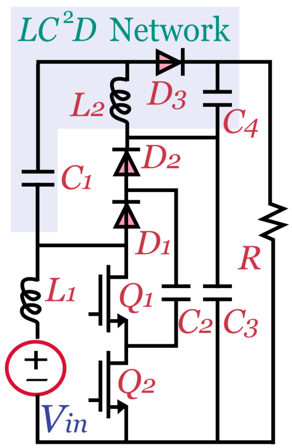
The proposed converter is presented in
Figure 2, where it is composed of two active switches (
Q1,
Q2), three diodes (
D1,
D2,
D3), two inductors (
L1,
L2), and four capacitors (
C1,
C2,
C3,
C4). The fuel cell is depicted as a dc voltage source (
Vin). The network of (
Q1,
Q2,
D1,
D2,
C2,
C3) forms a three-level flying-capacitor switching cell. The
LC2D output network enhances the voltage gain and reduces the voltage stress on the power switches.
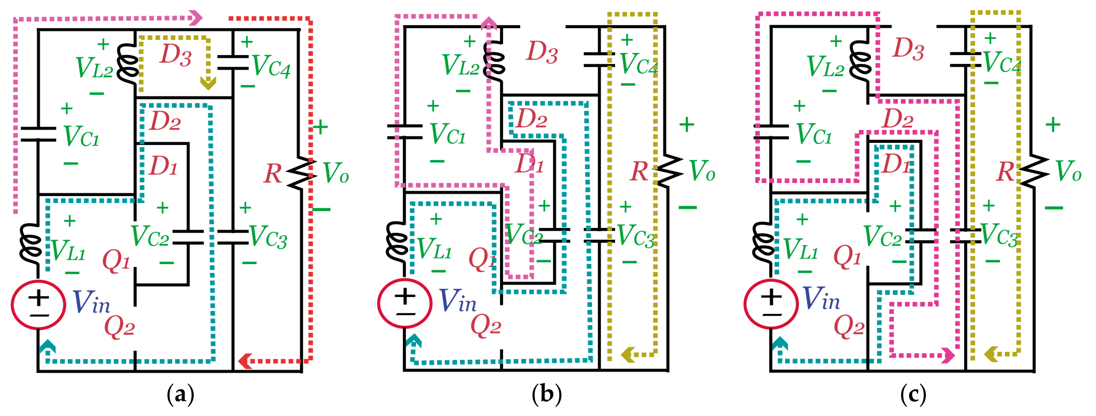
2.2. Operation Modes
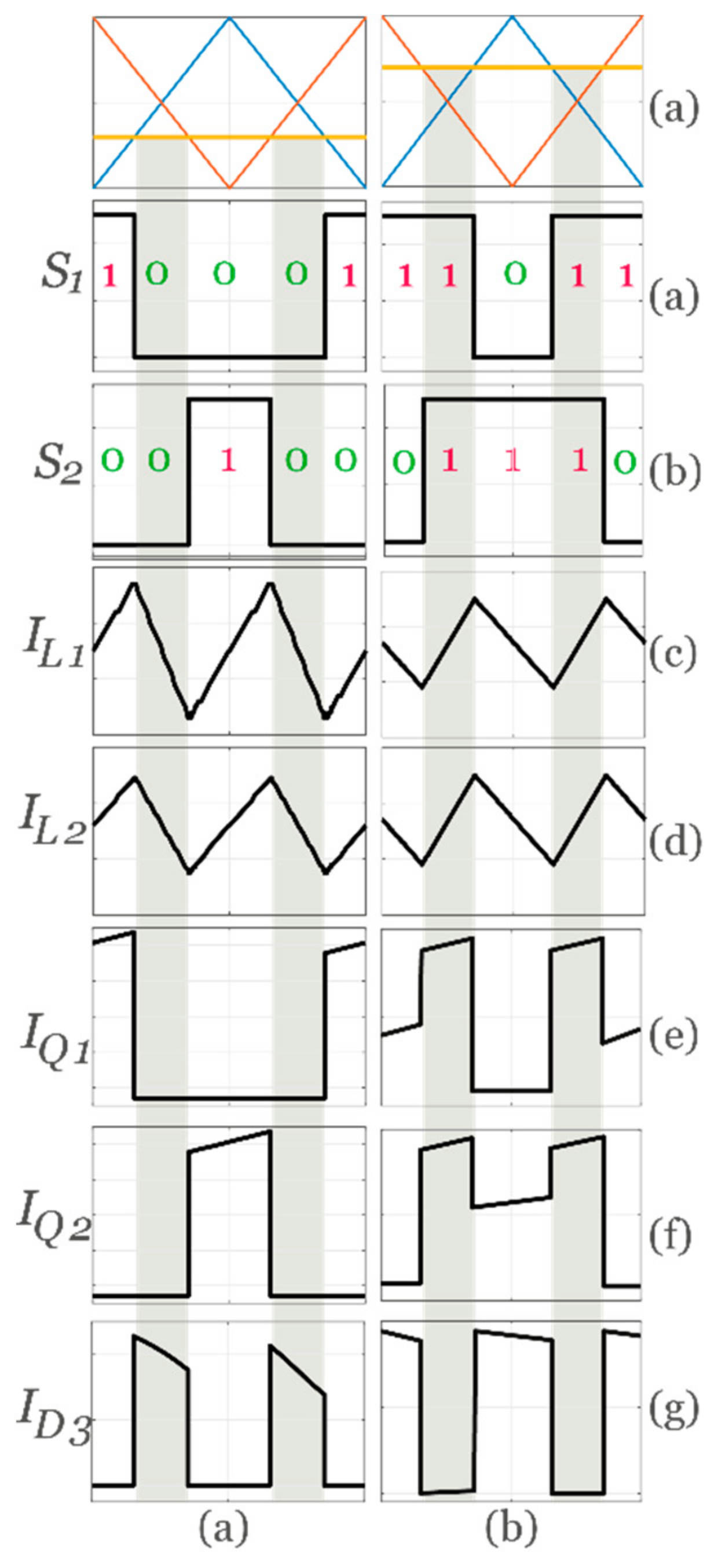
The proposed converter has two active switches; hence, it has four possible switching states for Q1 and Q2. These switching states are S1S2 = {00, 01, 10, and 11}, as S1 and S2 are the triggering signals of Q1 and Q2, respectively.
The triggering signals
S1 and
S2 are generated via comparing two phase-shifted 180° carrier signals with a modulation signal (
D). This means that there are three possible switching sequences based on the value of
D. When
D > 0.5, the switching sequence of
S1S2 is {10, 11, 01, 11, and 10}. When
D < 0.5, the switching sequence of
S1S2 is {10, 00, 01, 00, and 10}. When
D = 0.5, the switching sequence of
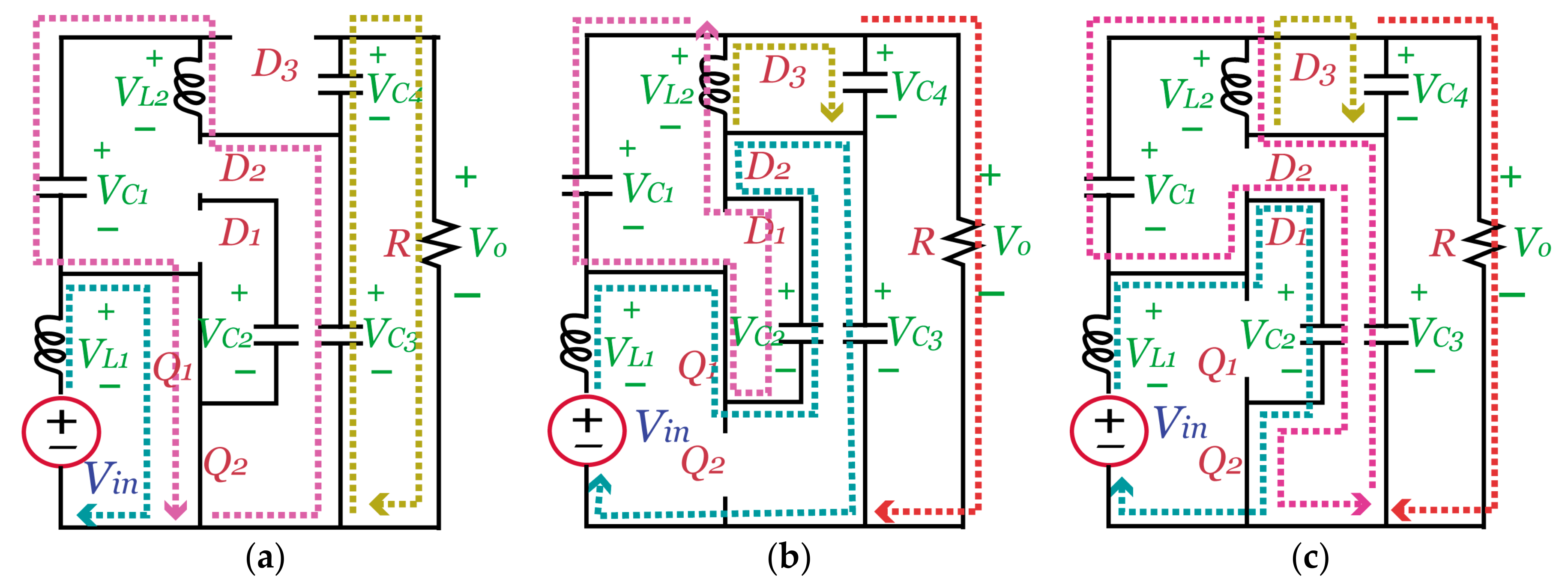
S1S2 is {10, 01, and 10}. The current flow paths when
D < 0.5 and
D > 0.5 are shown in
Figure 3 and
Figure 4, respectively, and the key waveforms of the proposed TLB converter are presented in
Figure 5.
2.3. Analysis of the Switching States
In this subsection, the proposed converter is analyzed during each of the four switching states to be used after that in calculating the voltage gain and the voltage stress associated with each switching sequence.
When
S1S2 = 01, as shown in
Figure 3c and
Figure 4c, by applying the Kirchhoff’s voltage law (KVL), we obtain Equations (1) and (2).
When
S1S2 = 10, as shown in
Figure 3b and
Figure 4b, by applying the KVL, we obtain Equations (3) and (4).
When
S1S2 = 11, as shown in
Figure 4a, by applying the KVL, we obtain Equations (5) and (6).
When
S1S2 = 00, as shown in
Figure 3a, by applying the KVL, we obtain Equations (7) and (8).
2.4. Wide Voltage Gain
In this subsection, the voltage gain of the proposed converter is derived for
D > 0.5 and
D < 0.5. To simplify the analysis, all the inductors and capacitors are assumed to be ideal and very large to apply the small ripple approximation. When
D > 0.5, as shown in
Figure 6b, the switching sequence of
S1S2 is {10, 11, 01, 11, and 10}. In this switching sequence the time of state {01},
T01, the time of state {10},
T10, and the time of state {11},
T11, are defined as shown in Equation (9):
As T is the periodic time of the carrier signals.
By applying the volt-second balance rule on
L1 and
L2, we obtain Equations (10) and (11):
The output voltage
Vo can be defined as the biggest value of the sum of “
VC3” and “
VL2”. Thus, when
D > 0.5,
Vo can be calculated as the following:
Because
C2 and
C3 are the two capacitors of a three-level flying capacitor network,
VC2 is half
VC3; hence, the following is true:
By substituting by Equations (10) and (11) in Equation (13), we obtain the following:
Thus, the voltage gain,
M, is defined by Equation (15) as follows:
When
D < 0.5, as shown in
Figure 6a, the switching sequence of
S1S2 is {10, 00, 01, 00, and 10}. In this switching sequence
T01,
T10, and the time of state {00},
T00, are defined as follows:
By applying the volt-second balance rule on
L1 and
L2, we obtains Equations (17) and (18):
In this switching sequence
Vo can be defined as the biggest value of the sum of “
VC3” and “
−VL2”. Thus, when
D < 0.5,
Vo can be calculated as the following:
By substituting by Equations (17) and (18) in Equation (19), we obtain the following:
Thus, the voltage gain,
M, is defined by Equation (21):
The equations derived for the D > 0.5 case can be applied for D = 0.5.
When
S1S2 is {10, or 01}, the states of
L1 and
L2 depend on the value of
D. From Equations (1)–(4), the voltage across
L1 and
L2 can be defined as the following:
By means of Equations (22) and (23) and the voltage polarities shown in
Figure 3 and
Figure 4, both
L1 and
L2 are charging when
D is less than 0.5, while they are discharging when
D is greater than 0.5.
2.5. Voltage Stress Analysis
2.5.1. Voltage Stress across the Capacitors
The voltages across
C4 equals (
Vo −
VC3). The voltages across
C1,
C2, and
C3 are described by Equations (24) and (25) as follows:
2.5.2. Voltage Stress across the Semiconductor Devices
The voltage across
Q1,
Q2,
D1,
D2, and
D3 can be expressed by Equation (26).
2.6. Current Stress Analysis
In this subsection the current stresses on both the semiconductor devices and inductors are derived. The analysis is divided into two parts, depending on the value of D. In the following equations, the output load current is Io, the average currents of inductors L1 and L2 are IL1 and IL2, respectively, the average charging currents of capacitors C1, C2, C3, and C4 are IC1_ch, IC2_ch, IC3_ch, and IC4_ch, respectively, and the average discharging currents of capacitors C1, C2, C3, and C4 are IC1_disch, IC2_disch, IC3_disch, and IC4_disch, respectively.
2.6.1. For D > 0.5
The current stresses can be obtained as follows.
In the
S1S2 = 11 switching state,
C3 discharges,
C1 charges,
C2 neither charges nor discharges, and
C4 discharges. Diode
D3 is reverse biased. By applying Kirchhoff’s current law (KCL), the relationships between the inductor and capacitor currents can be expressed as follows:
In the
S1S2 = 10 switching state,
C3 charges,
C1 discharges,
C2 discharges, and
C4 charges. Diode
D3 is forward biased. Thus, we obtain the following equations:
In the
S1S2 = 01 switching state,
C3 discharges,
C1 discharges,
C2 charges, and
C4 charges. Diode
D3 is forward biased. We obtain the following equations:
By using the capacitor charge-second balance rule on capacitors
C1,
C2,
C3, and
C4, the following relationships can be obtained:
Assuming a lossless operation, the relationship between
Io and
IL1 can be obtained as follows:
When
D > 0.5, diode
D3 conducts only during
S1S2 = {10, and 10}, and the instantaneous current flowing through
D3 during
T01 and
T10 is
ID3. During
S1S2 = {11}, the instantaneous current flowing through
Q1 and
Q2 is
IQ_11. During
S1S2 = {10}, the instantaneous currents flowing through
Q1,
Q2,
D1, and
D2 are
IQ1_10,
IQ2_10,
ID1_10, and
ID2_10, respectively. During
S1S2 = {01}, the instantaneous currents flowing through
Q1,
Q2,
D1, and
D2 are
IQ1_01,
IQ2_01,
ID1_01, and
ID2_01, respectively.
The root-mean-square (rms) values of currents flowing through the components of the converter are essential for loss analysis. The rms values of
IQ1,
IQ2,
ID1,
ID2,
ID3,
IC1,
IC2,
IC3, and
IC4 are
IQ1_rms,
IQ2_rms,
ID1_rms,
ID2_rms,
ID3_rms,
IC1_rms,
IC2_rms,
IC3_rms, and
IC4_rms, respectively. Using Equations (9), (27)–(46) we can obtain the following equations:
2.6.2. For D < 0.5
The current stresses can be obtained as follows.
In the
S1S2 = 00 switching state,
C3 charges,
C1 discharges,
C2 neither charges nor discharges, and
C4 charges. Diode
D3 is forward biased. By applying the KCL rule, the relationships between the inductor and capacitor currents can be expressed as follows:
In the
S1S2 = 10 switching state,
C3 charges,
C1 charges,
C2 discharges, and
C4 discharges. Diode
D3 is reverse biased. We obtain the following equations:
In the
S1S2 = 01 switching state,
C3 discharges,
C1 charges,
C2 charges, and
C4 discharges. Diode
D3 is reverse biased. We obtain the following equations:
By using the capacitor charge-second balance rule on capacitors
C1,
C2,
C3, and
C4, the following relationships can be obtained:
Assuming a lossless operation and using Equation (41), the relationship between
Io and
IL1 can be obtained by the following:
When
D < 0.5, diode
D3 conducts only during
S1S2 = {00}, and the instantaneous current flowing through
D3 during
T00 is
ID3_00. During
S1S2 = {00}, the instantaneous current flowing through
D3 is
ID3_00. The relationship between the transistor, diode, and inductor currents can be obtained by the following:
Using Equations (16), (52)–(66) the rms values of the transistor, diode, and capacitor currents can be expressed as the following:
2.7. Comparison with Other Multilevel Step-Up Converters
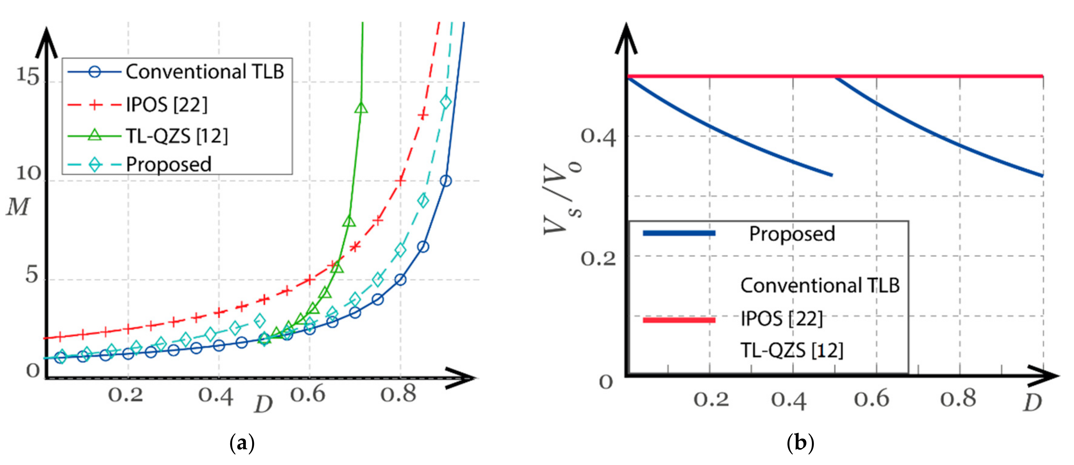
Based on the derived Equations (15), (21), and (26), which define the voltage gain and stress of the proposed converter, comparative analysis can be made between the proposed converter and other multilevel converters, as shown in
Table 1. In this comparison, the proposed converter is compared with the conventional TLB converter, a three-level quasi-z-source (TL-QZS) converter in [
9], and an input-parallel-output-series (IPOS) converter in [
24].
The conventional TLB converter has an ideal voltage gain of 1/(1-
D). The voltage stress across the semiconductor devices of the conventional TLB converter is
Vo/2. In [
9], this converter has a voltage gain of 2/(3-4
D), and the voltage stress across the semiconductor devices is
Vo/2. The duty cycle of this converter is limited between 50% and 75%, which makes the converter very sensitive to any change in duty. In [
24], the converter discussed in this paper has a voltage gain of 2/(1-
D), and the voltage stress across the power switches is
Vo/2.
Table 1 presents a peer-to-peer comparison between the proposed converter, the TL-QZS converter in [
9], and the IPOS converter in [
24].
Figure 6a,b show a comparison of the voltage gain
M versus duty cycle
D and the normalized voltage stress (
Vs/
Vo) versus
D among the four converters, respectively. This comparison shows that the proposed converter has a higher voltage gain compared with the conventional TLB converter. The TL-QZS converter has a higher voltage gain compared with the proposed converter, but the main drawback for the TL-QZS converter is its limited operational range (0.5 ≤
D < 0.75). The IPOS converter in [
24] has the highest voltage gain; however, the proposed converter has the least voltage stress on the semiconductor devices, which means that it can be built using semiconductor devices with lower rated voltage, leading to higher efficiency, and a lower cooling system requirement and hence, higher power density.
From Equation (26), the stress voltage in the proposed converter depends on both Vo and D, and the stress voltage swings between 50% of Vo and 33.33% of Vo.
4. Loss Analysis
The losses in the proposed converter can be divided into the following major contributors, namely: conduction and switching losses of the transistors Q1 and Q2, losses of the diodes D1, D2, and D3, losses of the inductors (L1 and L2), and losses of the capacitors (C1, C2, C3, and C4).
4.1. Conduction and Switching Losses of Transistors
Because the rms currents flowing through
Q1 and
Q2 are the same, as shown in Equations (47) and (68), and assuming that both transistors have the same on-resistance,
Ron, the total conduction loss of both
Q1 and
Q2 can be calculated by Equation (84) as follows
In a typical transistor, there are four major contributors to the switching loss, namely: (1) the overlap of the transistor current and voltage at the instant of turning on and off; (2) gate charge losses, which is caused by the charge stored in the gate capacitance; (3) the loss caused by the parasitic capacitance of the transistor, which is caused by the energy stored in
COSS when the transistor is off; and (4) the loss caused by the reverse recovery charge of the body diode of the transistor (because the experimental work was implemented with GaN E-HEMTs, which do not have body diodes and have zero reverse recover charges, this loss component can be neglected). Equation (85) describes the total switching loss of the two transistors of the proposed converter, where
fs is the switching frequency,
tr and
tf are the rise and fall times of the transistor, respectively,
QT is the gate charge, and
VG is the gate driver voltage. The drain-to-source voltage of the E-HEMTs equals half
VC3 and is thus depicted as
VC2.
4.2. Diode’s Losses
Because the experimental setup is implemented using SiC Schottky diodes, the reverse recovery switching loss of the diodes is neglected; however, the loss caused by the capacitive charge (
QC) of the Schottky diodes is considered. The conduction loss of these diodes depends on the forward voltage and the rms currents flowing through the diodes. Equation (86) calculates the total losses of the three diodes of the proposed converter:
where
Vfd and
QC are the forward voltage and the total capacitive charge of the SiC diode, respectively.
4.3. Inductors’ Losses
The inductors have two main loss components, namely the conduction loss, and the core loss. The conduction loss is caused by the dc current component flowing in the inductors’ windings, while the core loss is caused by the inductors’ ripple currents. The core loss equation should be provided by the core manufacturer. The inductors’ total conduction loss,
PL_cond, can be calculated using Equation (87), the inductors’ core loss,
PL_core, can be calculated using Equation (88), and the total losses in the inductors,
PL_tot, can be calculated using Equation (89).
where
RL1 and
RL2 are the series parasitic resistances of
L1 and
L2, respectively.
Equation (88) is provided by “Micrometals” (the manufacturer of the inductor cores used in the experimental prototype), where the equation’s parameters can be derived from the datasheet of each specific core size and dimension:
4.4. Capacitors’ Losses
The losses of the capacitors in the proposed converter are calculated as the conduction loss of these capacitors caused by their equivalent series resistance (ESR). The power loss of the four capacitors of the proposed converter,
PC, is expressed by Equation (90), where
ESRC1,
ESRC2,
ESRC3, and
ESRC4 are the equivalent series resistances of the four capacitors.
5. Experimental Results and Analysis
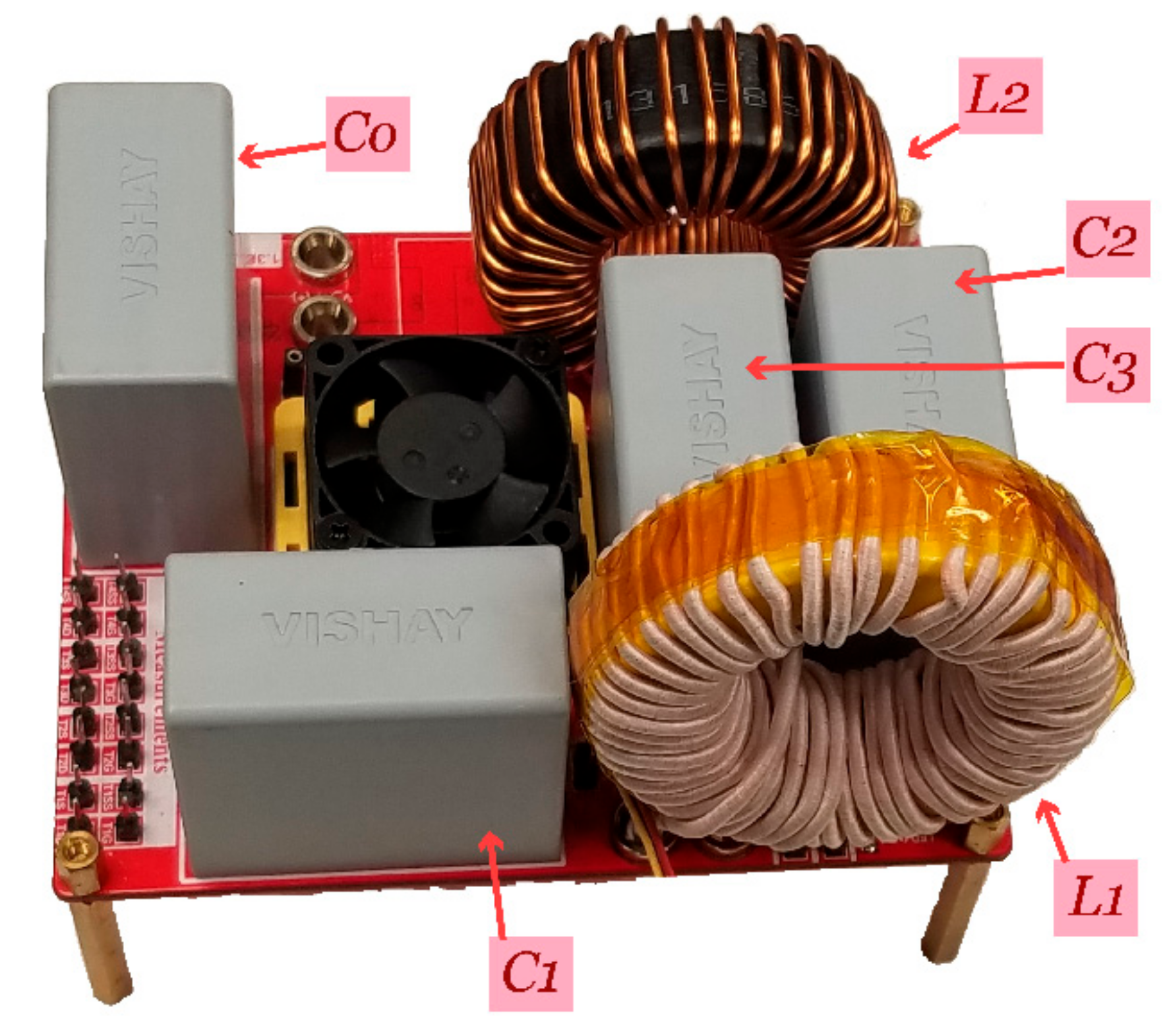
A scaled-down experimental prototype was built, as shown in
Figure 7, in order to validate the proposed converter topology and its theoretical analysis. In this experimental work, the fuel cell is depicted by a dc-voltage source. The converter is controlled by a TMS320f28377s microcontroller, and the currents are sensed by a hall-effect current transducer ACS730KLCTR-40AB-T. The power circuit is constructed using GS66508T E-HEMTs (rated voltage is 650 V, and rated current is 30 A) and C3D10065E SiC Schottky diodes (rated voltage is 650 V, and rated current is 32 A). The switching frequency,
fs, is 100 kHz, and the values of the two inductors
L1 and
L2 are 350 µH and 250 µH, respectively. The capacitors
C1,
C2,
C3, and
C4 have the same value (capacitance = 80 µF, and rated dc-voltage = 700 V). The load is represented by a 120 Ω resistance,
RL. The main experimental parameters of the proposed converter prototype are shown in
Table 3.
In this experimental work, two case studies are investigated:
- (1)
Case study I: Vin = 200 V, D = 0.3, RL = 120 Ω; and
- (2)
Case study II: Vin = 100 V, D = 0.7, RL = 120 Ω
The experimental results of case study I are intended to verify the theoretical analysis of the converter when
D < 0.5 and are presented in
Figure 8, while the experimental results of case study II are intended to verify the theoretical analysis of the converter when
D > 0.5 and are presented in
Figure 9.
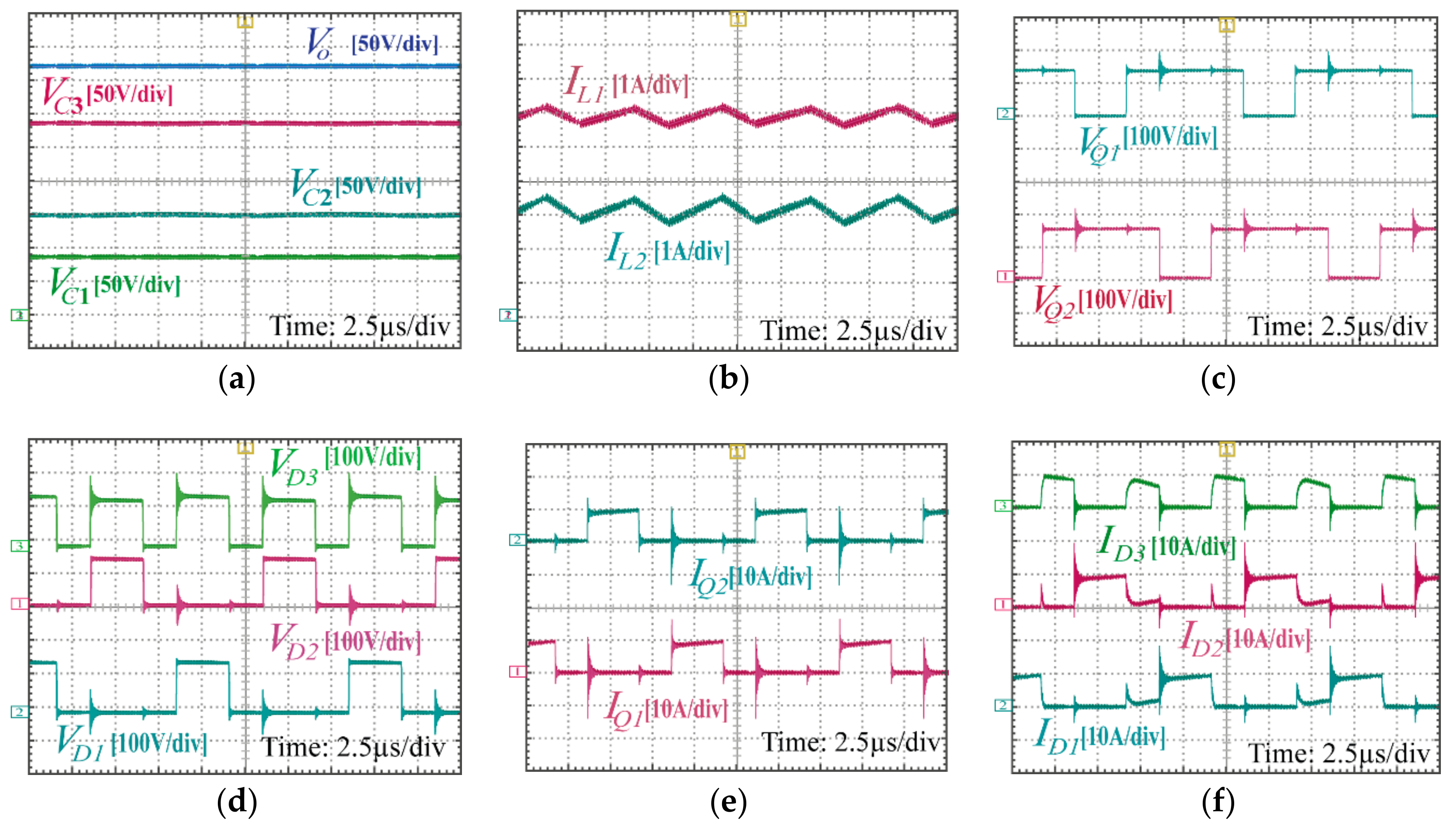
5.1. Case Study I (D = 0.3, Vin = 200 V, RL = 120 Ω)
When
D is less than 0.5, Equations (18), (20), and (24) describe the four capacitors’ voltages, and hence, they can be calculated as the following:
VC1 = 85.7 V,
VC2 = 142.9 V,
VC3 = 285.7 V, and
Vo = 371.4 V.
Figure 8a validates these findings. The two inductor currents,
IL1 and
IL2, are shown in
Figure 8b, and the frequency of the ripple currents is 200 kHz, which is double the switching frequency. The currents flowing through the two inductors
IL1 and
IL2, are close to 5.5 A and 3 A, respectively, which comply with the theoretical Equations (64) and (70). The voltage stresses across the E-HEMTs (
Q1 and
Q2) and the diodes (
D1,
D2, and
D3) are shown in
Figure 8c,d, respectively, where the voltage stresses swing between 0 V and 140 V (=
VC2), which comply with Equation (26).
Figure 8e,f show the currents flowing through the E-HEMTs, and the diodes, where the currents of (
Q1,
Q2,
D1, and
D2) swing between 0 A and 9 A, which comply with Equations (66) and (67). Also,
Figure 8e shows
ID3, where
D3 conducts only when both
Q1 and
Q2 are off, and the magnitude of
ID3 during conduction is close to 7.5 A, which complies with Equation (65). It is worth noting that the semiconductor devices should be selected with higher rated voltage and current to assure operating in the safe operation area (SOA) of these devices and account for the voltage spikes (caused by the parasitic inductance of the PCB) and current spikes (caused by the parasitic capacitance of the SiC Schottky diodes).
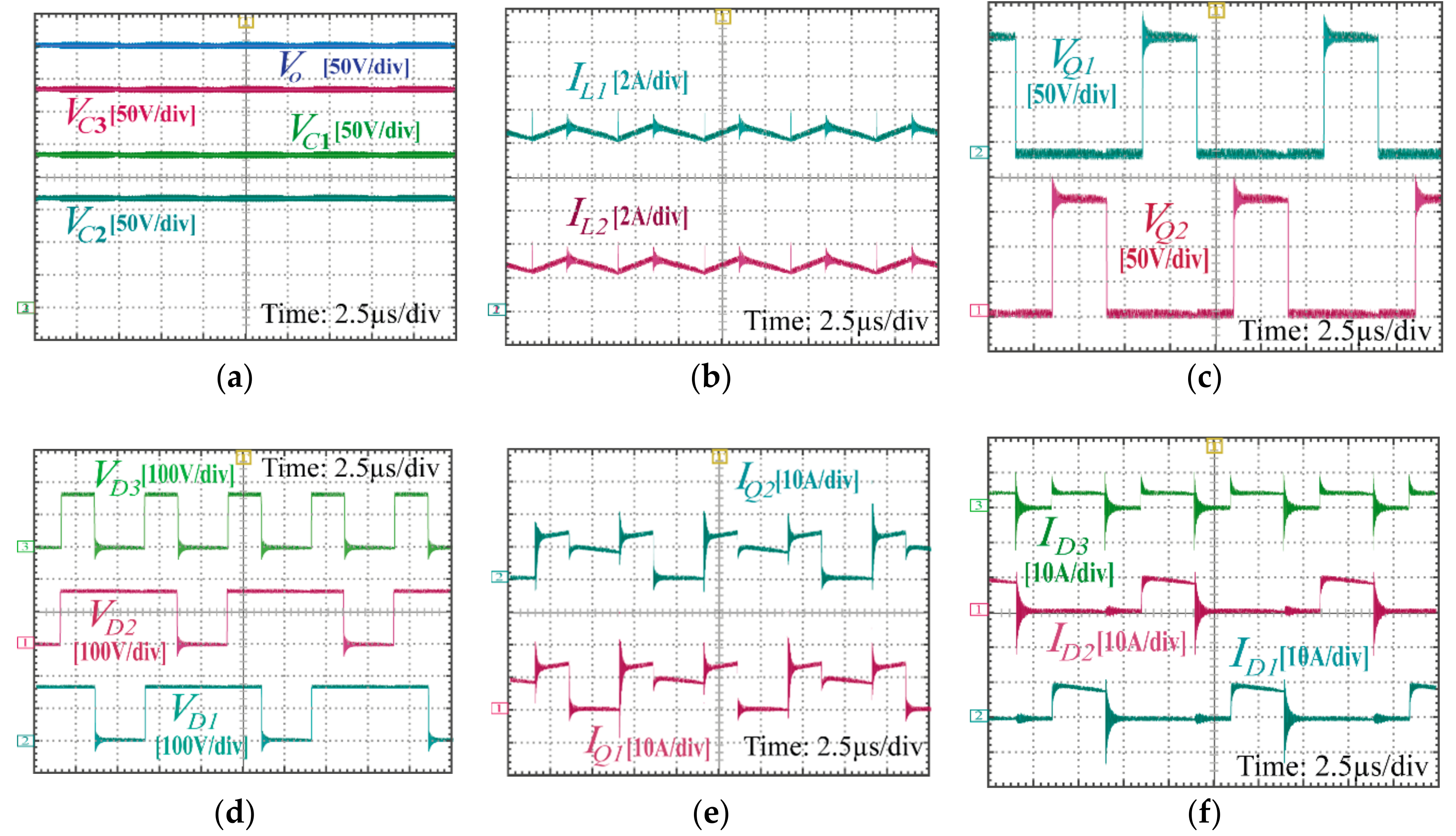
5.2. Case Study II (D = 0.7, Vin = 100 V, RL = 120 Ω)
From Equations (11), (15), and (24), the voltage across the four capacitors can be calculated as follows:
VC1 = 233.33 V,
VC2 = 166 V,
VC3 = 333 V, and
Vo = 400 V. These findings are verified by
Figure 9a.
Figure 9b shows the currents flowing through the two inductors,
IL1 and
IL2, which have ripple currents with frequencies equal to double the switching frequency of the converter (the periodic time of the ripple currents = 5 µS, and the periodic time of the switching = 10 µS). From
Figure 9b,
IL2 is close to 3.3 A, and
IL1 is close to 13 A, which verify Equations (40) and (42).
Figure 9c,d show the voltage stress across the E-HEMTs (
Q1 and
Q2) and the diodes (
D1,
D2, and
D3), respectively, where the voltage stress swings between 0 V and 166 V, namely between 0 V and half the voltage across
C3, which verifies Equation (26). The currents of the E-HEMTs (
Q1 and
Q2) are shown in
Figure 9e; each current swings between three levels, 0 A (the E-HEMT is off, and the other one is on), 11 A (the E-HEMT is on, and the other one is off), and 16 A (both of the E-HEMTs are on), which verify Equations (37), (44), and (45).
Figure 9e,f show the currents flowing through the diodes (
D1,
D2, and
D3). From Equations (45) and (46), diode
D1 conducts only when
S1S2 = {01}, while diode
D2 conducts only when
S1S2 = {10}, and the magnitude of the current flowing during conduction =
IL1 − ((2
D − 1)
IL2/(2
D − 2)) = 11 A, which is verified by
Figure 9f.
Figure 9e shows that
D3 conducts only when either of the E-HEMTs is off, and the current flowing during conduction is close to 6 A, which verifies Equation (43).
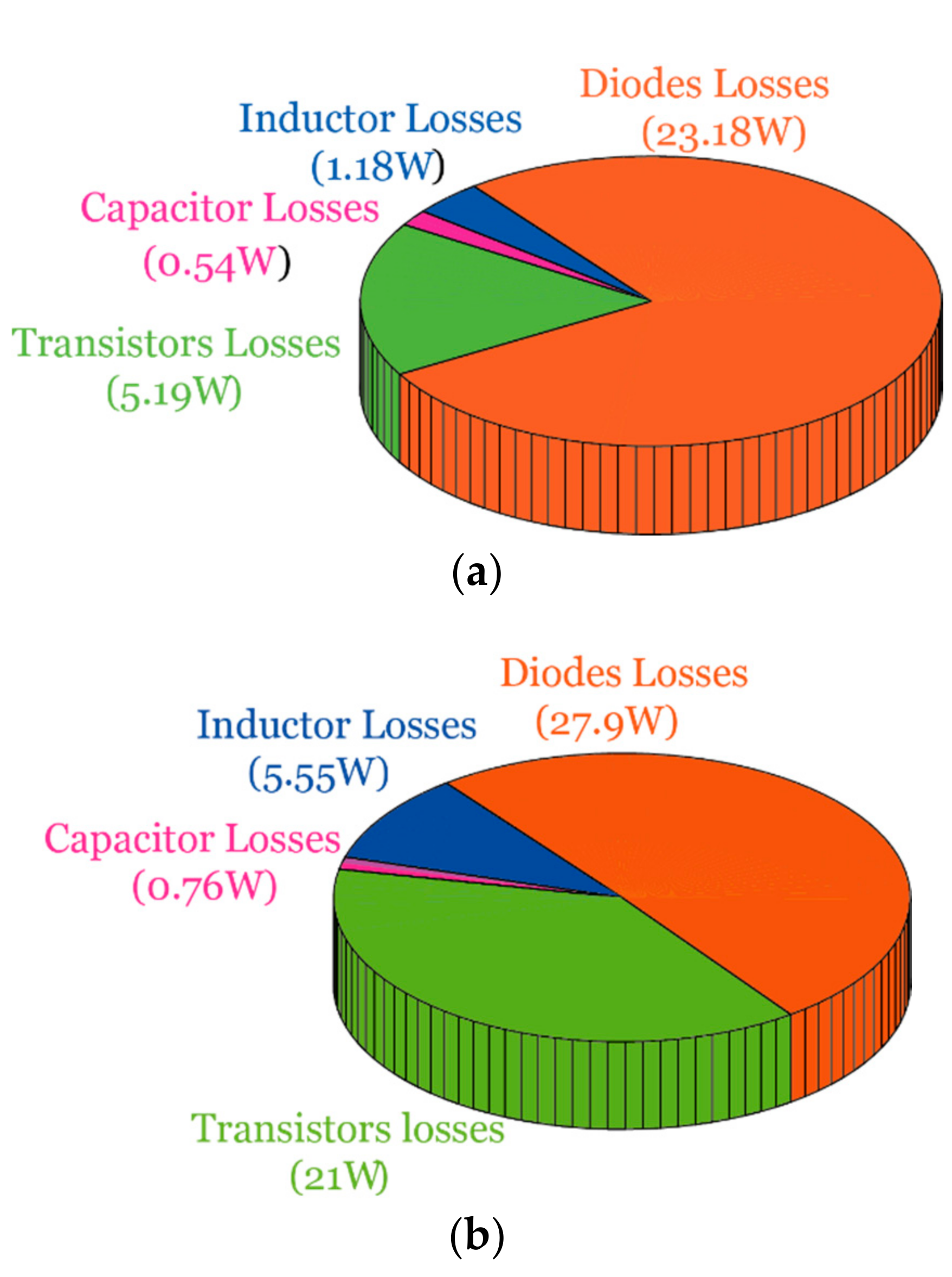
5.3. The Loss Analysis of the Proposed Converter
Using Equations (84)–(90), the losses of the proposed converter can be calculated for any value of
Vin,
D, and
RL. The converter losses for case studies I and II are investigated and analyzed.
Figure 10 shows the loss distributions for the proposed converter for both case study I and case study II.
Figure 10a shows the loss distributions when
D = 0.3,
Vin = 200 V, and
RL = 120 Ω,
Pout = 1.15 kW. The total losses of the converter in this case study equal 27.16 W, and the efficiency of the converter equals 97.6%. The main contributor of losses in this case is the diodes (85.3% of total losses), because of their relatively high forward voltage (
Vfd) = 1.8 V. The total losses of the E-HEMTs are 19% of the total losses, and this is because of their low on-resistance and zero reverse recovery charges. The losses of the inductors and capacitors account for 4.3% and 2.8% of the total losses of the proposed converter, respectively.
Figure 10b shows the loss distributions when
D = 0.7,
Vin = 100 V, and
RL = 120 Ω,
Pout = 1.333 kW. The total losses of the converter in this case study equal 55.21 W, and the efficiency of the converter equals 95.86%. The main contributor of losses in this case is also the diodes (50.5% of total losses). The total losses of the E-HEMTs are 38% of the total losses. The losses of the inductors and capacitors account for 10% and 1.37% of the total losses of the proposed converter, respectively.
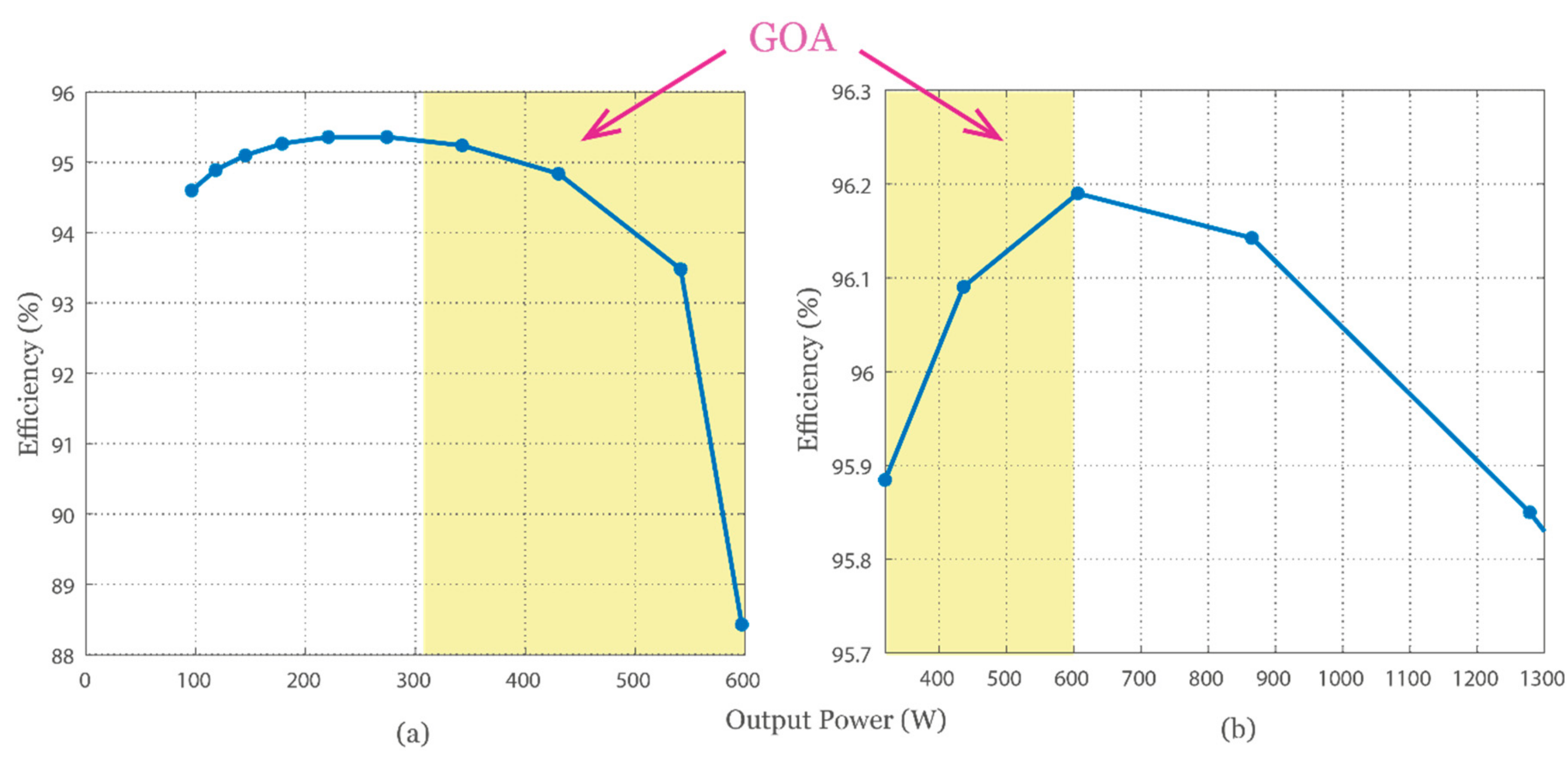
The efficiency curves of the proposed converter that depict the efficiency at different power levels are shown in
Figure 11, and they were obtained from the experimental setup (
Vin = 100 V,
fs = 100 kHz,
RL = 120 Ω). The efficiency is depicted by two curves, one for operation when
D < 0.5, and the other one for operation when
D ≥ 0.5.
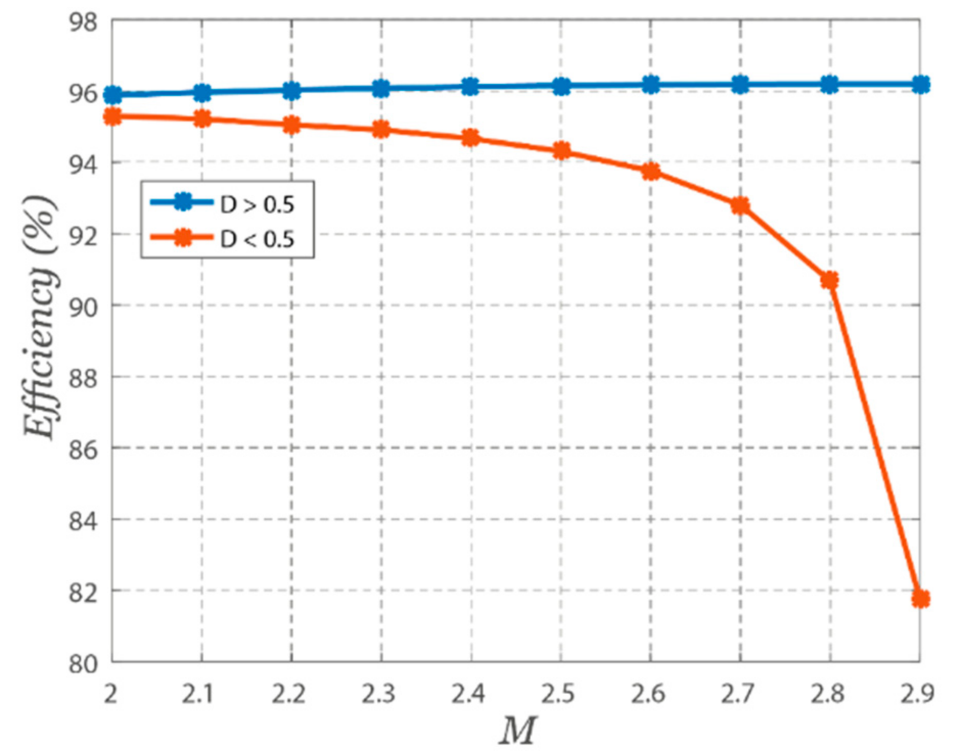
In the GOA, the same voltage gain (
M) can be achieved by two different values of
D; one of them is less than 0.5, and the other one is greater than 0.5.
Figure 12 shows the calculated efficiency of the proposed converter in the GOA. When
Vin = 100 V and
RL = 120 Ω, one curve presents the efficiency versus
M when
D is less than 0.5, while the other curve shows the efficiency versus
M when
D is greater than 0.5. From
Figure 12, it is obvious that if the desired
M is in the GOA (2 <
M < 3), the efficiency of the proposed converter is higher when
D is selected to be higher than 0.5.


