Abstract
In this work, we present a gettering technique for multicrystalline silicon (mc-Si) by combining a nanowire structure with thermal treatment under nitrogen in an infrared lamp furnace. The silicon nanowires were elaborated using the Silver Nanoparticles Chemical Etching (Ag-NPsCE) technique. The optimal conditions for achieving effective gettering were determined based on the minority carrier lifetime (τeff) measurements. The results show τeff as a function of the gettering temperature and etching time, both before and after the removal of Ag nanoparticles using HNO3. In both cases, the surface was identically treated with a 10% HF dip immediately prior to the carrier lifetime measurements. The highest τeff value, prior to Ag removal, was obtained after an etching duration of 3 min and was 6 µs at an excess carrier density Δn = 1 × 1014 cm−3. Moreover, τeff improves after silver removal. Therefore, removing Ag atoms using an aqueous HNO3 solution is necessary to prevent this issue. Following Ag nanoparticle removal, τeff further increases, reaching 19 µs at a gettering temperature of 850 °C. Similarly, the electrical conductivity (ρ) and carrier mobility (μ) improve significantly after gettering, where the resistivity increases from 5.5 Ω·cm for the reference mc-Si to 1.9 Ω·cm, and the mobility rises from 122 cm2·V−1·s−1 to 253 cm2·V−1·s−1 after nanowire-based gettering at 850 °C. Overall, this method provides a scalable, practical, and cost-effective route to optimize mc-Si for high-performance photovoltaic applications.
1. Introduction
Multicrystalline silicon (mc-Si) remains a dominant material in photovoltaic (PV) manufacturing due to its cost-effectiveness and proven compatibility with large-scale production [,], particularly when compared to other materials used in solar energy research [].
However, its electronic performance is inherently limited by structural defects, such as impurities, dislocations, grain boundaries [,,,], and residual metallic impurities (e.g., Fe, Cu, Ag) [,]. These imperfections act as potent recombination-active centers, which significantly reduce the minority carrier lifetime (τeff) and degrade carrier mobility (μ). Therefore, these defects increase electrical resistivity and severely constrain device efficiency. Typically, as-grown mc-Si exhibits a τeff value of only a few microseconds, μ of around 100–150 cm2·V−1·s−1, and electrical resistivity (ρ) of 5–6 Ω·cm [,], depending on the impurity levels and crystallographic quality. Such low electronic performance leads to substantial recombination losses and limits charge collection efficiency in PV devices. Among advanced photovoltaic (PV) technologies, one approach focuses on improving the optical, electrical, and optoelectronic performance of multicrystalline silicon wafers by combining bulk purification processes with targeted surface treatments [,,,]. Gettering is a critical purification technique designed to enhance the electronic quality of silicon substrates by relocating detrimental metal impurities from the active device region to a designated external site, such as in phosphorus diffusion gettering [], aluminum (Al) gettering [,], and SiNx gettering [,] at high-temperature annealing, all of which improve carrier lifetime and mobility but are often insufficient to address nanoscale defects, particularly at grain boundaries or near-residual metal clusters. This process, using silicon nanowires (Si NWs), serves as a form of sacrificial gettering [].
Gettering begins during high-temperature annealing as impurities are released from their initial states (precipitates, defect complexes), becoming mobile within the crystal lattice. These diffusing species then migrate toward the Si NWs surface, which acts as an efficient sink due to its high surface-to-volume ratio. Once captured through segregation or precipitation (e.g., metal silicide formation), the impurity-loaded surface layer is selectively removed (typically by chemical etching), thereby permanently eliminating the contaminants and significantly enhancing the substrate’s electronic quality.
This study aims to demonstrate the enhancement of the electronic quality of multicrystalline silicon (mc-Si) through the integration of silicon nanowires (SiNWs) with a high-temperature gettering annealing process conducted in a nitrogen atmosphere. The introduction of SiNWs onto the mc-Si surface significantly increases gettering efficiency due to their exceptionally large surface-to-volume ratios, which offer numerous energetically favorable sites for metallic impurity adsorption and immobilization. During annealing, these impurities are thermally driven toward the nanowire-rich surface, where they become trapped, thereby reducing their concentration within the bulk.
Following the treatment, the samples underwent comprehensive structural, optical, and optoelectronic characterization to evaluate the effectiveness of the SiNW-assisted gettering approach. Surface morphology and nanowire distribution were analyzed using scanning electron microscopy (SEM), providing direct insight into nanostructure uniformity and the formation of gettering-active regions. Reflectance measurements were carried out to assess surface texturing and light-trapping capabilities. Infrared (IR) absorption spectroscopy was employed to probe chemical bonding states and identify impurity- or oxide-related vibrational modes. Minority carrier lifetime measurements were performed to quantify the reduction in recombination-active centers and determine the overall improvement in bulk electronic quality. Furthermore, electrical conductivity and carrier mobility were evaluated using Hall effect measurements.
2. Results and Discussions
Figure 1 shows the effect of silicon nanowires (SiNWs) on the total reflectivity for an etching duration of 3 min. The reflectance spectra were measured using a UV–Vis–NIR spectrophotometer equipped with an integrating sphere. The untreated reference sample exhibits a total reflectivity of approximately 24%. After forming the mc-SiNWs via the Ag-NPsCE process, the reflectivity is substantially reduced, reaching values as low as 4% at 400 nm. Overall, the average reflectance decreases from roughly 29% for the bare silicon surface to about 7% for the SiNW surface, indicating a significant enhancement in light absorption due to the nanowire-based anti-reflective structure. This pronounced reduction demonstrates the effectiveness of nanostructuring in improving light trapping by increasing surface roughness and promoting multiple internal reflections through the large active surface area. Beyond photovoltaics, SiNWs are also utilized in various applications [], including biosensors [], photocatalysis [], and solar cells [].
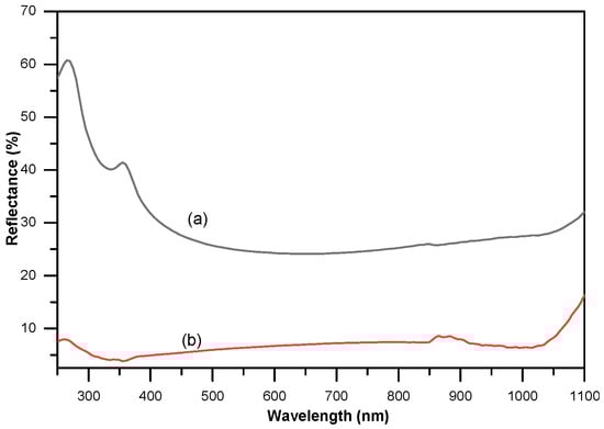
Figure 1.
Total reflectivity between (a) bare silicon and (b) SiNWs after 3 min etching.
Figure 2 displays the FTIR absorption spectrum of silicon nanowires (SiNWs) synthesized via the Ag-NPsCE technique for 3 min. The spectrum was recorded within the 400–1500 cm−1 frequency range. No characteristic bands are observed in the high-energy region, indicating the absence of significant functional groups in this range. In contrast, several prominent bands appear in the low-energy region, corresponding to silicon lattice vibrations Si–Si, silicon oxide bonds Si–O–Si, and surface hydride/hydroxyl terminations (see Table 1) such as SiO–H, Si–H2, and Si–OH. The Si–Si vibration is detected at 610 cm−1, while the Si–O–Si vibrations are detected at 450 cm−1, 736 cm−1, and within the 1000–1300 cm−1 range, whereas the SiO–H, Si–H2, and Si–OH bands appear at 810 cm−1, 880 cm−1, and 980 cm−1, respectively. The oxide-related vibrational bands show significantly higher intensities than the hydrogen-related bands. This difference is largely due to wet oxidation caused by the nitric acid used during the critical silver catalyst removal step. Furthermore, the low intensity of the Si–H2 bands is attributed to the release of hydrogen gas bubbles during the silicon nanowire (SiNWs) growth process []. All forms of oxidation, whether wet or natural, proceed through intermediate states (SiO–H and Si–OH), eventually forming a stable layer of fully oxidized SiO2.
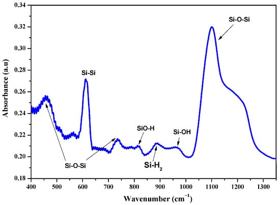
Figure 2.
FTIR absorption spectrum of mc-silicon nanowires.

Table 1.
Absorption bands of (Si–O–Si, Si–H, and Si–OH) along with corresponding references.
The effective minority carrier lifetime (τeff) of silicon nanowires (SiNWs) is intrinsically low, which often limits the feasibility of detailed lifetime evaluations. However, preliminary measurements show a pronounced dependence of τeff on the etching duration. Following SiNW formation via the Ag-NPsCE process, τeff decreases from 1.4 µs to 1.06 µs as the etching time is increased to 5 min. This degradation arises from three concurrent mechanisms as follows: (i) Extended carrier transport paths, resulting from the considerable nanowire length often exceeding 19 µm, leading to dense or irregular nanowire networks that create tortuous transport paths and increasing carrier trapping and scattering; (ii) surface recombination, caused by a high density of surface dangling bonds generated during chemical etching, which act as efficient non-radiative recombination centers; and (iii) defect-mediated trapping, resulting from residual silver nanoparticles (Ag-NPs) that remain partially embedded within or between the nanowires even after nitric acid cleaning, introducing deep-level trap states within the silicon bandgap. Consequently, surface recombination and defect-induced trapping processes are intrinsic to high-aspect-ratio SiNW architectures that predominantly dictate the reduction in τeff.
To mitigate current lifetime losses, an effective gettering strategy is essential for removing impurities and passivating defect sites. Concurrently, future work will focus on improving characterization accuracy by minimizing surface effects through superior passivation. This involves implementing a high-quality layer, such as Atomic Layer Deposition (ALD) Al2O3, onto the wafer surfaces. By utilizing this advanced passivation, we can effectively decouple surface recombination from residual Ag effects, allowing us to accurately quantify the true impact of metallic contamination on the carrier lifetime and guide further gettering optimization.
To improve the carrier lifetime, we employed an advanced gettering technique for multicrystalline silicon (mc-Si) that combines nanowire structuring with thermal treatment under a nitrogen atmosphere in an infrared lamp furnace. The SiNWs were fabricated using the Ag-NPsCE method, allowing precise control over their morphology and density. The main objective of this approach is to enhance impurity removal and defect passivation within the mc-Si substrate. To optimize gettering efficiency, process parameters—including etching duration, nanowire density, and thermal treatment conditions—were systematically evaluated based on τeff measurements. The results demonstrate that the combination of nanostructuring and controlled thermal treatment significantly increases τeff, indicating effective gettering of metallic impurities and a substantial reduction in recombination-active defects.
Multicrystalline silicon nanowire substrates underwent thermal annealing in a nitrogen N2 atmosphere using an infrared furnace to promote impurity gettering and defect passivation (see Figure 3).
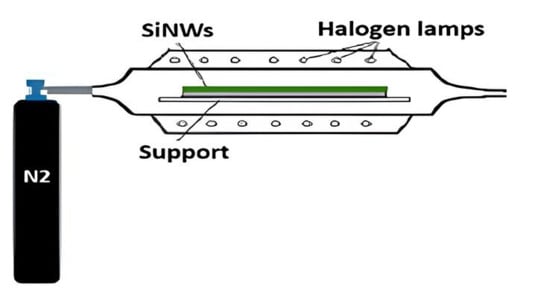
Figure 3.
Schematic of the IR-RTP setup used for thermal annealing of SiNWs.
Following the procedure described in the Experimental Section, samples were annealed at 850 °C and 900 °C for 60 min. The process employed a rapid ramp rate of 50 °C/s up to the peak temperature, followed by a cooling rate of 5 °C/s under a continuous N2 flow rate of 100 sccm. Samples were carefully spaced 1 cm apart within the furnace to ensure uniform heating.
Figure 4 shows the variation in τeff as a function of gettering temperature and etching time, both before and after Ag-NP removal using HNO3. Before Ag removal, the maximum τeff observed after 3 min of etching is 6 μs at an excess carrier density of Δn = 1 × 1014 cm−3. Notably, τeff increases substantially after Ag removal. At elevated temperatures, Ag atoms can diffuse into the silicon lattice, forming defect centers in combination with other impurities, which degrade the carrier lifetime. Therefore, removing Ag with an aqueous HNO3 solution is essential to prevent such effects. Following Ag-NP removal, τeff improves to 19 μs at 850 °C, demonstrating the effectiveness of the process in reducing recombination-active defects, and the results of this process are better than those reported in []. The observed improvement in τeff is primarily due to the migration of impurities from the mc-Si bulk into the sacrificial nanowire layer, where they are trapped and subsequently removed by immersion in a 1 M NaOH solution. This reduction in impurity concentration decreases electron–hole recombination centers, thereby enhancing τeff. However, at 900 °C, mc-Si nanowire gettering results in a decrease in τeff, down to 6 μs, at a carrier density of 1 × 1014 cm−3. This indicates that high-temperature accumulation is not desirable due to the competition between impurity extraction and impurity dissolution rates. Furthermore, the τeff degradation at 900 °C is hypothesized to be caused by the high annealing temperature promoting the formation of new crystallographic defects. These defects not only act as powerful recombination centers but also serve as physical barriers that impede impurity mobility toward the intended trapping region []. In our case, the SiNWs themselves may contribute to the formation of these defects, highlighting the necessity of investigating the effects of high temperatures on the morphology of mc-Si nanowires [].
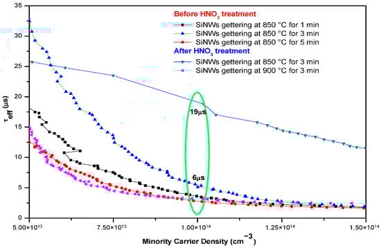
Figure 4.
Variation in τeff as a function of carrier density, after gettering of mc-Si nanowires (SiNWs) for different etching times at 850 °C and 900 °C.
In this section, the Hall effect measurements (Ecopia, HMS-5000, Bridge Technology, USA) operating within a temperature range of 80 K to 350 K (Figure 5) were used to assess the electrical properties of silicon after the gettering process. Since gettering, particularly when implemented via silicon nanowires (SiNWs), is designed to extract impurities and passivate bulk defects, it is expected to induce notable changes in the material’s electrical characteristics. Hall measurements of resistivity (ρ), carrier mobility (μ), and majority carrier concentration (n) provide direct evidence of the effectiveness of impurity removal and defect passivation.
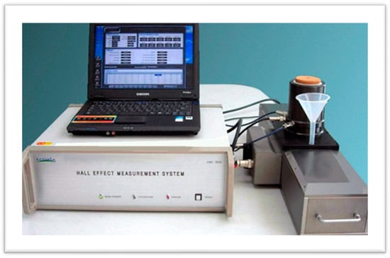
Figure 5.
The Hall effect measurement system used.
A successful gettering process is typically characterized by an increase in carrier mobility (μ) accompanied by a decrease in carrier concentration (n), reflecting the reduction in impurity scattering centers and recombination-active defects. Therefore, Hall effect analysis serves as an essential post-treatment validation step for quantifying the improvement in electronic quality resulting from SiNW-assisted gettering. The Hall data summarized in Table 2 confirm that the effect of a substantial increase in μ and a pronounced reduction in n are observed for the optimally treated sample. Specifically, the mc-Si sample subjected to nanowire gettering at 850 °C exhibited the most significant improvement, with ρ and μ evolving from 5.5 Ω·cm and 122 cm2·V−1·s−1 (reference sample) to 1.9 Ω·cm and 253 cm2·V−1·s−1, respectively. In contrast, the electrical parameters obtained after treatment at 900 °C are worse. This deterioration was attributed to the competition between impurity migration and trapping; at excessively high temperatures, trapped impurities may re-dissolve or diffuse back into the silicon bulk, while new crystallographic defects may form, both of which suppress carrier mobility and diminish the overall effectiveness of the gettering process.
Table 2.
Effect of mc-Si nanowire-based gettering on the electrical parameters.
3. Materials and Methods
In this work, Silicon Nanowires (SiNWs) were fabricated using Silver Nanoparticles Chemical Etching (Ag-NPsCE), a technique that enables precise control over nanowire length, density, and uniformity, where the schematic steps used in SiNW elaboration by the Ag-NPsCE method are explained in Figure 6. Beyond offering a highly reproducible nanowire morphology, the Ag-NPsCE process also generates catalytic sites that facilitate impurity diffusion during subsequent thermal treatments. The substrate used in this experimental process is a p-type mc-Si with a thickness of 300 µm and an area of 2 cm2, and a resistivity range of 0.5–2.0 Ω·cm was used in SiNW elaborations. The Ag-NPsCE technique involves depositing metallic nanoparticles (NPs) onto pre-cleaned Si substrates to ensure direct contact between the NPs and the silicon surface [].
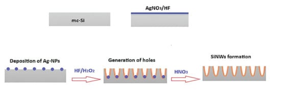
Figure 6.
Schematic steps used during SiNWs elaboration by Ag-NPsCE method.
Silver nitrate (AgNO3) is dissolved in an aqueous HF solution, releasing Ag+ ions according to Reaction (1):
The Ag+ ions are then reduced to metallic silver, which deposits spontaneously on the mc-Si surface via electroless metal deposition, without any external electrical energy. After optimization, the cleaned mc-Si substrates were first immersed in an HF/AgNO3 solution (4.8/0.02 M) at 25 °C for 2 min to deposit the Ag nanoparticles. In a second step, the Ag NP-coated substrates were immersed in an HF/H2O2 solution (4.8/0.2 M) for 3 min to etch the mc-silicon and form uniform SiNWs, as illustrated in Figure 7. Finally, the nanostructured samples were treated in a nitric acid (HNO3) bath to dissolve any residual Ag nanoparticles and induce wet oxidation of the mc-Si surface, forming a thin SiO2 layer. This oxide was subsequently removed by brief immersion in a 10% HF solution, leaving clean and well-defined silicon nanowires ready for further processing. The surface treatments were identical before and after Ag removal, consisting of a 10% HF dip immediately prior to the carrier lifetime measurements. No additional passivation layers (e.g., SiNx or Al2O3) were applied.
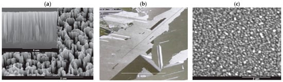
Figure 7.
Mc-SiNWs elaboration by the Ag-NPsCE: (a) ref mc-Si, (b) Ag-NPs distribution, and (c) top and cross section view of mc-SiNWs.
4. Conclusions
In this study, mc-SiNWs were successfully fabricated using the Ag-NPsCE technique, and their impact on carrier lifetime and gettering efficiency was systematically investigated. The formation of SiNWs initially leads to a reduction in the effective minority carrier lifetime due to increased surface recombination, dangling bonds, and residual silver nanoparticles. However, by combining nanowire structuring with thermal annealing under a nitrogen atmosphere, effective gettering of metallic impurities was achieved, resulting in a significant improvement in τeff and enhanced carrier mobility. The optimal results were obtained at 850 °C, where τeff increased to 19 μs, and Hall measurements exhibited the most significant improvement, with ρ and μ evolving from 5.5 Ω·cm and 122 cm2·V−1·s−1 (reference sample) to 1.9 Ω·cm and 253 cm2·V−1·s−1, respectively. Overall, this study demonstrates that integrating nanowire structuring with controlled thermal treatment provides an efficient strategy for impurity gettering and defect passivation in multicrystalline silicon. This approach offers a promising route to improve the electronic quality of silicon substrates for photovoltaic and electronic applications. However, a critical caveat emerged; optimization at 900 °C was detrimental, indicating that impurity dissolution and defect formation outweigh the benefits of gettering at this high temperature. Therefore, while τeff improvements confirm the material’s potential, this enhanced performance ultimately requires device-level validation before its benefits in functional solar cells can be fully realized.
Author Contributions
All authors contributed to this study’s conception and design. Conceptualization, A.M. and M.B.R.; methodology, A.M.; software, W.D.; validation, M.B.R., W.D. and K.C.; formal analysis, A.M.; investigation, M.B.R.; resources, W.D.; data curation, M.B.R.; writing—original draft preparation, M.B.R. and W.D.; writing—review and editing, M.B.R.; visualization, K.C.; supervision, W.D.; project administration, K.C.; funding acquisition, K.C. All authors have read and agreed to the published version of the manuscript.
Funding
This work was supported and funded by the Deanship of Scientific Research at Imam Mohammad Ibn Saud Islamic University (IMSIU) (grant number IMSIU-DDRSP2502).
Institutional Review Board Statement
Not applicable.
Informed Consent Statement
Not applicable.
Data Availability Statement
The datasets generated during and/or analyzed during the current study are available from the corresponding author upon reasonable request for privacy.
Conflicts of Interest
The authors declare no conflicts of interest.
References
- Burtescu, S.; Parvulescu, C.; Babarada, F.; Manea, E. The low cost multicrystalline silicon solar cells. Mater. Sci. Eng. B 2009, 165, 190–193. [Google Scholar] [CrossRef]
- Lan, C.W.; Hsu, C.; Nakajima, K. Multicrystalline silicon crystal growth for photovoltaic applications. In Handbook of Crystal Growth; Elsevier: Amsterdam, The Netherlands, 2015; pp. 373–411. [Google Scholar]
- Suchikova, Y.; Nazarovets, S.; Konuhova, M.; Popov, A.I. Binary Oxide Ceramics (TiO2, ZnO, Al2O3, SiO2, CeO2, Fe2O3, and WO3) for Solar Cell Applications: A Comparative and Bibliometric Analysis. Ceramics 2025, 8, 119. [Google Scholar] [CrossRef]
- Lv, X.; Li, H.; Ding, D.; Yu, X.; Jin, C.; Yang, D. Interfacial characterization of non-metal precipitates at grain boundaries in cast multicrystalline silicon crystals. J. Cryst. Growth 2025, 652, 128042. [Google Scholar] [CrossRef]
- Wang, L.; Liu, J.; Li, Y.; Wei, G.; Li, Q.; Fan, Z.; He, D. Dislocations in Crystalline Silicon Solar Cells. Adv. Energy Sustain. Res. 2024, 5, 2300240. [Google Scholar] [CrossRef]
- Chen, J.; Chen, B.; Lee, W.; Fukuzawa, M.; Yamada, M.; Sekiguchi, T. Grain boundaries in multicrystalline si. Solid State Phenom 2010, 156, 19–26. [Google Scholar] [CrossRef]
- Woo, S.; Bertoni, M.; Choi, K.; Nam, S.; Castellanos, S.; Powell, D.M.; Choi, H. An insight into dislocation density reduction in multicrystalline silicon. Sol. Energy Mater. Sol. Cells 2016, 155, 88–100. [Google Scholar] [CrossRef]
- Hu, D.; Zhang, J.; Yuan, S.; Chen, H.; Wang, C.; Yu, X.; Cheng, X. Effects of metal impurities at the edges of cast Si ingot on crystal quality and solar cell performance. Sol. Energy 2022, 246, 224–233. [Google Scholar] [CrossRef]
- Hu, Z.; Lin, D.; Yu, X.; Seiffert, C.; Kuznetsov, A.; Yang, D. Role of metal impurities in multicrystalline silicon solar cell degradation. Appl. Phys. Express 2021, 14, 115502. [Google Scholar] [CrossRef]
- Cuevas, A.; Forster, M.; Rougieux, F.; Macdonald, D. Compensation engineering for silicon solar cells. Energy Procedia 2012, 15, 67–77. [Google Scholar] [CrossRef]
- Wenham, S.R.; Green, M.A.; Watt, M.E.; Corkish, R.; Sproul, A. Applied Photovoltaics; Routledge: London, UK, 2013. [Google Scholar] [CrossRef]
- Alrasheedi, N.H. The effects of porous silicon and silicon nitride treatments on the electronic qualities of multicrystalline silicon for solar cell applications. Silicon 2024, 16, 1765–1773. [Google Scholar] [CrossRef]
- Almeshaal, M.A.; Abdouli, B.; Choubani, K.; Khezami, L.; Rabha, M.B. Study of porous silicon layer effect in optoelectronics properties of multi-crystalline silicon for photovoltaic applications. Silicon 2023, 15, 6025–6032. [Google Scholar] [CrossRef]
- Ogundipe, O.B.; Okwandu, A.C.; Abdulwaheed, S.A. Recent advances in solar photovoltaic technologies: Efficiency, materials, and applications. GSC Adv. Res. Rev. 2024, 20, 159–175. [Google Scholar] [CrossRef]
- Khezami, L.; Jemai, A.B.; Alhathlool, R.; Rabha, M.B. Electronic quality improvement of crystalline silicon by stain etching-based PS nanostructures for solar cells application. Sol. Energy 2016, 129, 38–44. [Google Scholar] [CrossRef]
- Dasilva-Villanueva, N.; Catalán-Gómez, S.; Marrón, D.F.; Torres, J.J.; García-Corpas, M.; del Cañizo, C. Reduction of trapping and recombination in upgraded metallurgical grade silicon: Impact of phosphorous diffusion gettering. Sol. Energy Mater. Sol. Cells 2022, 234, 111410. [Google Scholar] [CrossRef]
- Porre, O.; Martinuzzi, S.; Pasquinelli, M.; Perichaud, I.; Gay, N. Gettering effect of aluminium in mc-Si and c-Si wafers and in solar cells. In Proceedings of the Conference Record of the Twenty Fifth IEEE Photovoltaic Specialists Conference, Washington, DC, USA, 13–17 May 1996. [Google Scholar]
- Achref, M.; Bessadok, A.J.; Khezami, L.; Mokraoui, S.; Benrabha, M. Effective surface passivation on multi-crystalline silicon using aluminum/porous silicon nanostructures. Surf. Interfaces 2020, 18, 100391. [Google Scholar] [CrossRef]
- Liu, A.; Sun, C.; Sio, H.C.; Zhang, X.; Jin, H.; Macdonald, D. Gettering of Transition Metals in High-Performance Multicrystalline Silicon by Silicon Nitride Films and Phosphorus Diffusion. J. Appl. Phys. 2019, 125, 043103. [Google Scholar] [CrossRef]
- Sun, C.; Liu, A.; Samadi, A.; Chan, C.; Ciesla, A.; Macdonald, D. Transition Metals in a Cast-Monocrystalline Silicon Ingot Studied by Silicon Nitride Gettering. Phys. Status Solidi RRL 2019, 13, 1900456. [Google Scholar] [CrossRef]
- Amri, C.; Ouertani, R.; Hamdi, A.; Ezzaouia, H. Enhancement of electrical parameters in solar grade monocrystalline silicon by external gettering through sacrificial silicon nanowire layer. Mater. Res. Bull. 2018, 98, 41–46. [Google Scholar] [CrossRef]
- Feng, Y.; Zhao, S.; Liang, P.; Xia, Z.; Peng, H. Application of silicon nanowires. Curr. Nanosci. 2025, 21, 373–384. [Google Scholar] [CrossRef]
- Biswas, P.; Karn, A.K.; Balasubramanian, P.; Kale, P.G. Biosensor for detection of dissolved chromium in potable water: A review. Biosens. Bioelectron. 2017, 94, 589–604. [Google Scholar] [CrossRef] [PubMed]
- Algethami, F.K.; Trabelsi, K.; Hajjaji, A.; Rabha, M.B.; Khezami, L.; Elamin, M.R.; El Khakani, M.A. Photocatalytic activity of silicon nanowires decorated with PbS nanoparticles deposited by pulsed laser deposition for efficient wastewater treatment. Materials 2022, 15, 4970. [Google Scholar] [CrossRef]
- Chehata, N.; Ltaief, A.; Beyou, E.; Ilahi, B.; Salem, B.; Baron, T.; Bouazizi, A. Functionalized silicon nanowires/conjugated polymer hybrid solar cells: Optical, electrical and morphological characterizations. J. Lumin. 2015, 168, 315–324. [Google Scholar] [CrossRef]
- Feng, R.; Liu, Y.; Li, S.; Chen, H.; Song, C.; Tao, P.; Shang, W. Hydrogen evolution from silicon nanowire surfaces. RSC Adv. 2018, 8, 41657–41662. [Google Scholar] [CrossRef]
- Ellerbrock, R.H.; Stein, M.; Schaller, J. Comparing silicon mineral species of different crystallinity using Fourier transform infrared spectroscopy. Front. Environ. Chem. 2024, 5, 1462678. [Google Scholar] [CrossRef]
- Arad-Vosk, N.; Sa’ar, A. Radiative and nonradiative relaxation phenomena in hydrogen- and oxygen-terminated porous silicon. Nanoscale Res. Lett. 2014, 9, 47. [Google Scholar] [CrossRef]
- Niu, J.; Yang, D.; Sha, J.; Wang, J.N.; Li, M. Infrared spectra of silicon nanowires. Mater. Lett. 2007, 61, 894–896. [Google Scholar] [CrossRef]
- Chen, Z.H.; Tang, Y.B.; Liu, Y.; Kang, Z.H.; Zhang, X.J.; Fan, X.; Lee, C.S.; Bello, I.; Zhang, W.J.; Lee, S.T. Dye degradation induced by hydrogen-terminated silicon nanowires under ultrasonic agitations. J. Appl. Phys. 2009, 105, 034307. [Google Scholar] [CrossRef]
- Philip, J.L. Infrared Analysis of Organsilicon Compounds: Spectra-Structure Correlations Silicon Compounds: Silanes and Silicones; Gelest Inc.: Morrisville, PA, USA, 2013. [Google Scholar]
- Gupta, P.; Dillon, A.C.; Bracker, A.S.; George, S.M. FTIR studies of H2O and D2O decomposition on porous silicon surfaces. Surf. Sci. 1991, 245, 360–372. [Google Scholar] [CrossRef]
- Kato, S.; Yamazaki, T.; Kurokawa, Y.; Miyajima, S.; Konagai, M. Influence of fabrication processes and annealing treatment on the minority carrier lifetime of silicon nanowire films. Nanoscale Res. Lett. 2017, 12, 242. [Google Scholar] [CrossRef]
- Hsueh, T.J.; Chen, H.Y.; Tsai, T.Y.; Weng, W.Y.; Yeh, Y.M.; Dai, B.T.; Shieh, J.M. Si nanowire-based photovoltaic devices prepared at various temperatures. IEEE Electron Device Lett. 2010, 31, 1275–1277. [Google Scholar] [CrossRef]
- Karyaoui, M.; Bardaoui, A.; Rabha, M.B.; Harmand, J.C.; Amlouk, M. Effect of rapid oxidation on optical and electrical properties of silicon nanowires obtained by chemical etching. Eur. Phys. J.-Appl. Phys. 2012, 58, 20103. [Google Scholar] [CrossRef]
Disclaimer/Publisher’s Note: The statements, opinions and data contained in all publications are solely those of the individual author(s) and contributor(s) and not of MDPI and/or the editor(s). MDPI and/or the editor(s) disclaim responsibility for any injury to people or property resulting from any ideas, methods, instructions or products referred to in the content. |
© 2025 by the authors. Licensee MDPI, Basel, Switzerland. This article is an open access article distributed under the terms and conditions of the Creative Commons Attribution (CC BY) license (https://creativecommons.org/licenses/by/4.0/).