Simultaneous Multi-Channel Microwave Photonic Signal Processing


1
Department of Electrical and Computer Engineering, McGill University, Montreal, QC H3A 0E9, Canada
2
Department of Physics, CEGEP Vanier College, St. Laurent, QC H4L 3X9, Canada
*
Author to whom correspondence should be addressed.
Photonics 2017, 4(4), 44; https://doi.org/10.3390/photonics4040044
Submission received: 25 October 2017
/
Revised: 11 November 2017
/
Accepted: 15 November 2017
/
Published: 17 November 2017
(This article belongs to the Special Issue Microwave Photonics 2017)
Abstract
:Microwave photonic (MWP) systems exploit the advantages of photonics, especially with regards to ultrabroad bandwidth and adaptability, features that are significantly more challenging to obtain in the electronic domain. Thus, MWP systems can be used to realize a number of microwave signal processing functions including, amongst others, waveform generation and radio-frequency spectrum analysis (RFSA). In this paper, we review recent results on fiber and integrated approaches for simultaneous generation of multiple chirped microwave waveforms as well as multi-channel RFSA of ultrahigh repetition optical rate pulse trains.
1. Introduction
Microwave photonics (MWP) unites the disciplines of microwave engineering with optoelectronics, and focuses on the use of photonic techniques and technologies to generate, process, and analyze/characterize microwave signals or to obtain radio-frequency (RF) characteristics of optical signals [1,2,3]. Photonics provides ultrabroad bandwidth and supports parallelization and adaptiveness (e.g., to achieve reconfiguration and tuning); thus, MWP enables a number of important functions in microwave systems that are either too complex or not possible to implement with conventional electronic approaches. Over the years, applications of MWP have evolved to include, amongst others, communications (e.g., to support the interface of wireless and optical communications, as well as for emerging 5G communications and the Internet of Things), sensing (e.g., to enhance resolution and increase the interrogation speed of conventional fiber optic sensor systems), and instrumentation (e.g., wideband signal characterization). To support these various applications, numerous functions are required, such as photonic generation of arbitrary waveforms, e.g., microwave, millimeter wave, and THz signals [4,5]; photonic processing of microwave signals, e.g., filtering, time delay, and phase shifting [6,7,8]; and photonic characterization of microwave signals, e.g., spectrum analysis and instantaneous frequency measurement (IFM) [9,10].
Chirped microwave waveforms have been used widely in various applications, especially radar systems [11]. Photonic generation of chirped microwave waveforms offers the possibility to obtain central frequencies of tens to hundreds of GHz as well as significant RF chirp rates, thereby supporting tens of GHz of bandwidth [4,5]. Photonic approaches also provide increased flexibility, especially in terms of tuning the central frequency and/or RF chirp rate of the waveforms. Such features and capabilities are not generally possible or have limitations with electronics. A variety of photonic approaches have been explored for RF arbitrary waveform generation and, in particular, chirped microwave waveforms. Most implementations demonstrated to date are capable of only generating a single waveform at a time, i.e., of a specific central frequency or RF chirp rate. On the other hand, the ability to obtain simultaneously multiple chirped microwave waveforms, each having its own characteristics, may enhance flexibility and provide new functionality in instrumentation and imaging applications. In this paper, we describe two fiber-based implementations for simultaneous generation of multiple (at least two) chirped microwave waveforms. The first approach uses superimposed linearly chirped Bragg gratings (BGs) in a Sagnac interferometer while the second incorporates multiple linearly chirped BGs in a multi-channel arrayed waveguide Sagnac interferometer (AWGSI). We show how these structures can be used to synthesize multiple chirped microwave waveforms with the same central frequency and different RF chirp rates, as well as to obtain independent control over the central frequency and RF chirp rates.
Electrical spectrum analysis of ultrabroadband photonic RF arbitrary waveforms and ultrahigh repetition rate optical pulse trains is necessary for monitoring the quality of the waveforms. It is performed typically using a photodiode for optical-to-electrical (O/E) conversion and an electrical spectrum analyzer (ESA). However, this approach is limited by the bandwidth of available electronics and, hence, cannot be used to characterize photonic waveforms that have a bandwidth in excess of 100 GHz. While a trade-off between measurement bandwidth and resolution has to be made, photonic implementation of radio-frequency spectrum analysis (RFSA) based on ultrafast nonlinear optics (e.g., Kerr nonlinearity) allows for characterizing signals with a bandwidth well beyond 100 GHz. Photonic RFSA was originally proposed and demonstrated using optical fiber as the nonlinear medium [12]; it has since been reported using integrated technologies in chalcogenide, silicon-on-insulator, and silica material platforms [13,14,15,16,17]. In all demonstrations, however, only a single waveform can be characterized at a time. Simultaneous multi-channel (or multi-signal) RFSA with a single integrated device may be more practical compared to using (and duplicating) multiple nonlinear waveguides for parallel single channel operation. Integrated waveguides can be engineered to support several propagating spatial modes, which we can exploit to perform multi-channel nonlinear optical signal processing, including RFSA. This creates a new degree of freedom for scaling the number of channels that can be characterized simultaneously. In this paper, we describe how to harness nonlinear optics in a mode selective manner using an integrated silicon photonic (SiP) device, ultimately leading to the realization of on-chip multi-channel RFSA.
2. Photonic Generation of Chirped Microwave Waveforms
2.1. General Considerations
There are many different techniques that use photonics for arbitrary microwave waveform generation. A relatively straightforward and powerful approach is to perform optical pulse shaping to synthesize the desired optical (temporal) waveform followed by O/E conversion (see Figure 1a). The ability to tailor the optical pulses translates into the ability to realize reconfigurable and tunable microwave waveform generation. A number of optical pulse shaping techniques exist, including classical Fourier transform pulse shaping, direct space-to-time pulse shaping, temporal pulse shaping, and optical spectral shaping followed by wavelength-to-time mapping (WTM) [4,18]. In terms of ease of implementation, the latter approach is very attractive: a spectral shaper is used to tailor the amplitude spectrum from a pulsed broadband optical source and the shaped spectrum then propagates through a dispersive medium where the frequency content is distributed in the time domain, i.e., WTM, see Figure 1b [4,19].
To generate a uniform microwave waveform, i.e., with constant frequency or that is chirp-free, we require a spectral shaper that has a periodic filter response, i.e., a constant free spectral range (FSR), and a linear WTM. On the other hand, to obtain a chirped microwave waveform, we can follow one of two approaches: (1) use a spectral shaper with a constant FSR and a nonlinear WTM [20,21] or (2) use a spectral shaper with a variable FSR followed by a linear WTM. While both approaches have been demonstrated, we consider the second, as it avoids the need for specially designed dispersive media with nonlinear delay characteristics or the limitations of such media, e.g., group delay ripple associated with nonlinearly chirped BGs. Moreover, a simple length of single-mode fiber (SMF) or dispersion compensating fiber (DCF) can implement linear WTM over a broad optical bandwidth. It should be noted that the principle component in the systems for generating chirped microwave waveforms is the spectral shaper: it must allow for synthesizing the desired amplitude spectrum from the input source, as this will ultimately correspond to the desired waveform after WTM.
2.2. Photonic Generation of Chirped Microwave Waveforms Using Superimposed LCFBGs
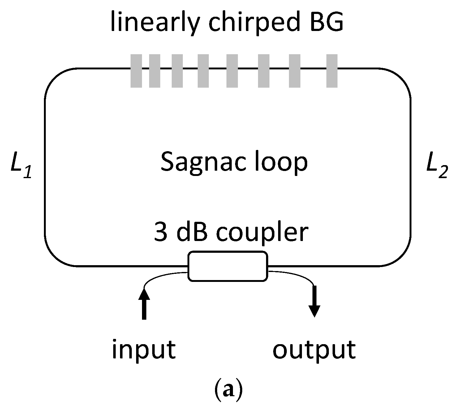
Spectral shapers in both fiber and integrated forms that provide an aperiodic response (i.e., variable FSR) have been considered, including a serial array of BGs (sometimes referred to as a spatially discrete chirped BG or a step-chirped BG) [22,23], a Fabry–Pérot cavity with distributed resonances based on spatially separate or overlapping (either fully or partially) linearly chirped BGs [24,25], a Michelson interferometer incorporating linearly chirped BGs in each arm [26,27], or a Sagnac interferometer incorporating a single linearly chirped BG [28,29]. The Sagnac configuration, illustrated in Figure 2a, provides the same functionality as the Michelson interferometer incorporating two identical and oppositely chirped BGs. Unlike the serial array or Fabry-Pérot cavity with distributed resonances, the spectral response of the Sagnac interferometer can be tuned readily by adjusting the path mismatch in the loop. Moreover, the configuration is simple, as it requires only a single grating and is robust to environmental perturbations. The spectral response of the Sagnac interferometer incorporating a linearly chirped BG is given by [4,30]:
where Rg(λ) is the reflectivity of the grating, neff is the effective index of the waveguide, CLCBG is the linear chirp of the grating (in nm/mm or nm/cm), ∆L = L1 − L2 is the path mismatch between the two arms in the Sagnac interferometer, and λc is the center wavelength. The spectral response has a wavelength dependent FSR defined by
where denotes the wavelength dependent, equivalent cavity length. After linear WTM in a dispersive medium with a first-order dispersion coefficient (in units of ps/nm), the instantaneous frequency of the microwave waveform can be approximated by
and the corresponding RF chirp rate is
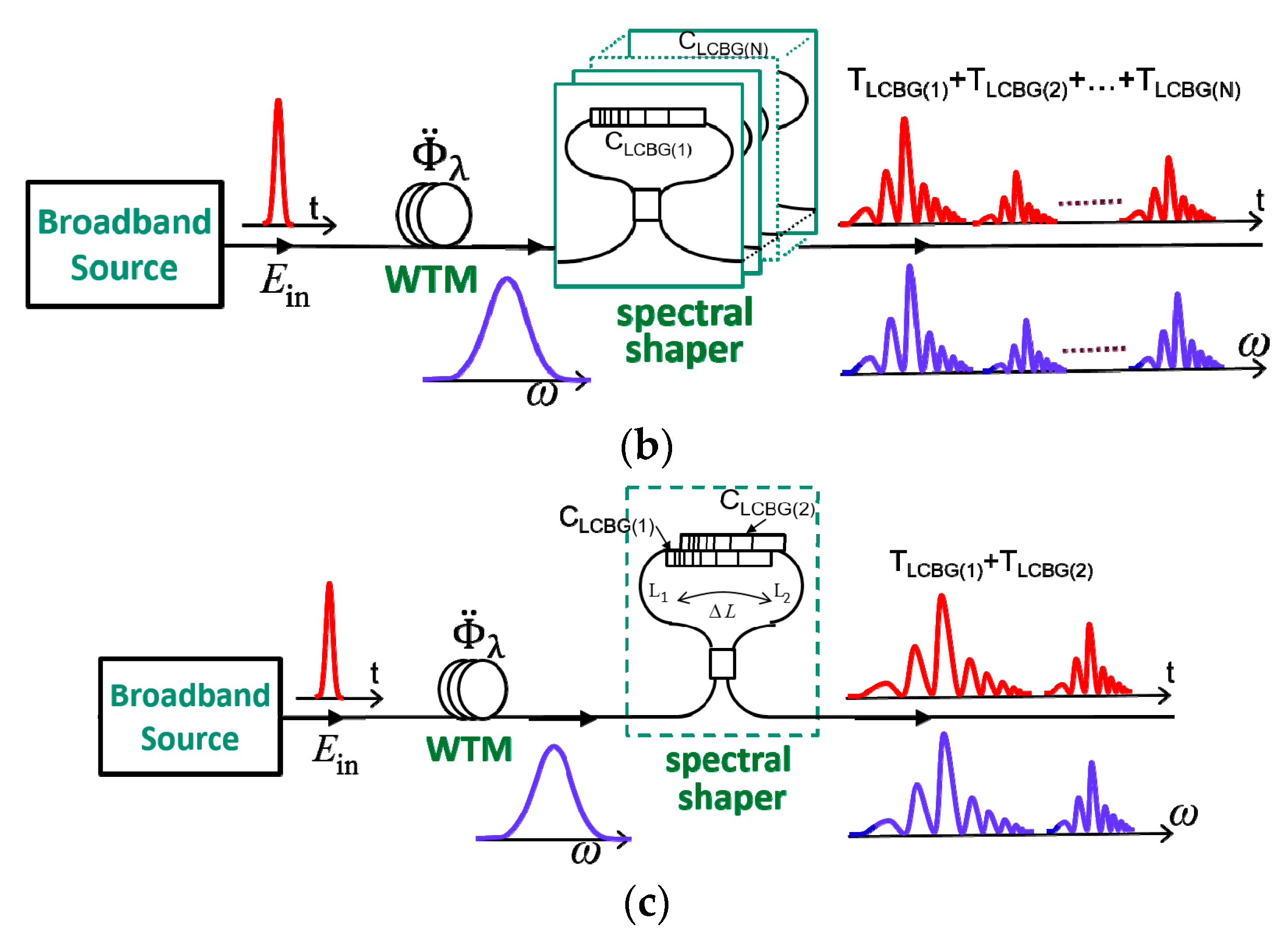
A single linearly chirped BG in a Sagnac interferometer provides a single aperiodic spectral response (within the grating bandwidth), which can be used to generate a single chirped microwave waveform. In order to generate multiple chirped microwave waveforms simultaneously, we require multiple spectral shapers, e.g., multiple or parallel Sagnac interferometers, each incorporating their own linearly chirped BG as illustrated in Figure 2b. As shown in Figure 2c, we can replace the multiple Sagnac interferometers and multiple linearly chirped BGs by a single Sagnac interferometer incorporating superimposed linearly chirped BGs to achieve the same functionality [31]. The superimposed gratings operate over different spectral bands and hence, operate independently. As such, the structure can be considered equivalent to multiple Sagnac interferometers operating in parallel whereby each one generates a single chirped microwave waveform. A drawback of this configuration, though, is that the superimposed gratings all have the same path mismatch.
Equations (1)–(4) are also valid for the case of superimposed gratings. The spectral response effectively comprises multiple spectral bands, each associated with the response of one of the gratings in the superimposed structure. Moreover, the characteristics of each spectral band, and hence the properties of the chirped microwave waveform that can be generated, are determined by the corresponding grating in the superimposed structure. As shown by Equations (3) and (4), for a fixed WTM, the central frequency of each chirped microwave waveform, given by , depends on the path mismatch ∆L (r the corresponding delay time , where c0 is the speed of light in vacuum) while the RF chirp rate depends only on the grating chirp (CLCBG). As all of the gratings experience the same path mismatch, all of the generated chirped microwave waveforms have the same central frequency. Moreover, if the superimposed gratings have the same chirp, then the generated microwave waveforms will also have the same RF chirp rate. On the other hand, if the superimposed gratings have different chirps, then we can obtain chirped microwave waveforms having the same central frequency, but with different values of RF chirp rate.
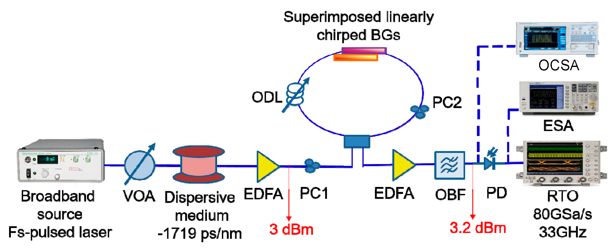
To demonstrate the principle, we generate simultaneously two chirped microwave waveforms using a fiber-based Sagnac interferometer incorporating two superimposed linearly chirped BGs. Figure 3 depicts the experimental setup. We use a femtosecond mode-locked laser operating at a repetition rate of 20 MHz (corresponding to a period of 50 ns) as the broadband source. WTM is achieved using a length of DCF with a dispersion of = −1719 ps/nm. The two superimposed gratings have the same reflectivity of ~80%; the central wavelengths are 1545.4 nm and 1551.1 nm (the spectral separation is ~5.7 nm), the corresponding 3 dB bandwidths are 4.4 nm and 4.9 nm, and the dispersions are CLCBG1 = 53.3 ps/nm and CLCBG2 = 47.8 ps/nm. Erbium doped fiber amplifiers (EDFAs) are used to compensate for losses. The average power of the broadband pulses launched into the Sagnac interferometer is ~3 dBm. We use polarization controllers (PCs) to adjust and optimize the interference pattern of the Sagnac response and one tunable optical delay line (ODL) to adjust the delay time or path mismatch between the two arms. By adjusting the ODL, we can readily obtain waveforms at different central frequencies (as described by Equation (3)) in real time. Prior to O/E conversion, we remove amplified spontaneous emission (ASE) noise from the EDFAs using an optical bandpass filter (OBF). We measure the spectral responses of the generated waveforms using an optical complex spectrum analyzer (OCSA) having a resolution of 0.16 pm and record the temporal waveforms using a high bandwidth photodiode (PD) for O/E conversion connected to a 33 GHz real-time oscilloscope (RTO) operating at 80 GS/s. After O/E conversion, we also obtain the RF spectra using a 40 GHz ESA with a resolution bandwidth of 20 kHz (we use optical filters to separate spectrally the two waveforms prior to measuring their RF spectra). Note that, since the system for generating the waveforms is linear, the order in which the two operations—spectral shaping and WTM—are performed does not matter; in our experiments, we perform WTM prior to spectral shaping.
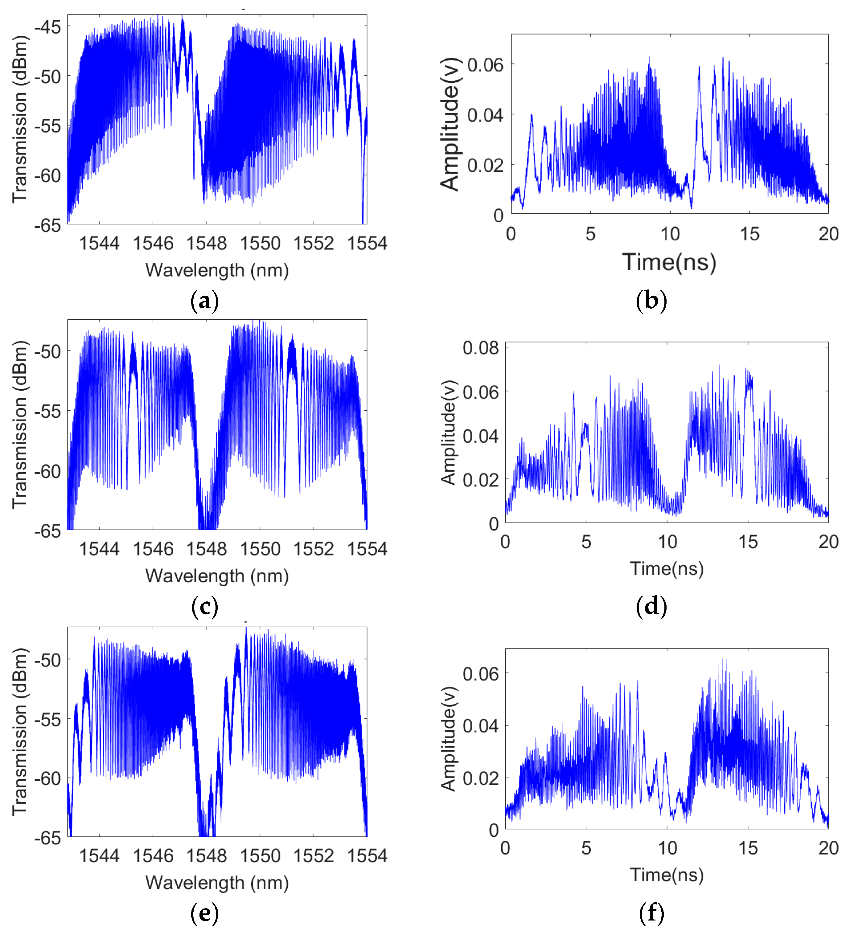
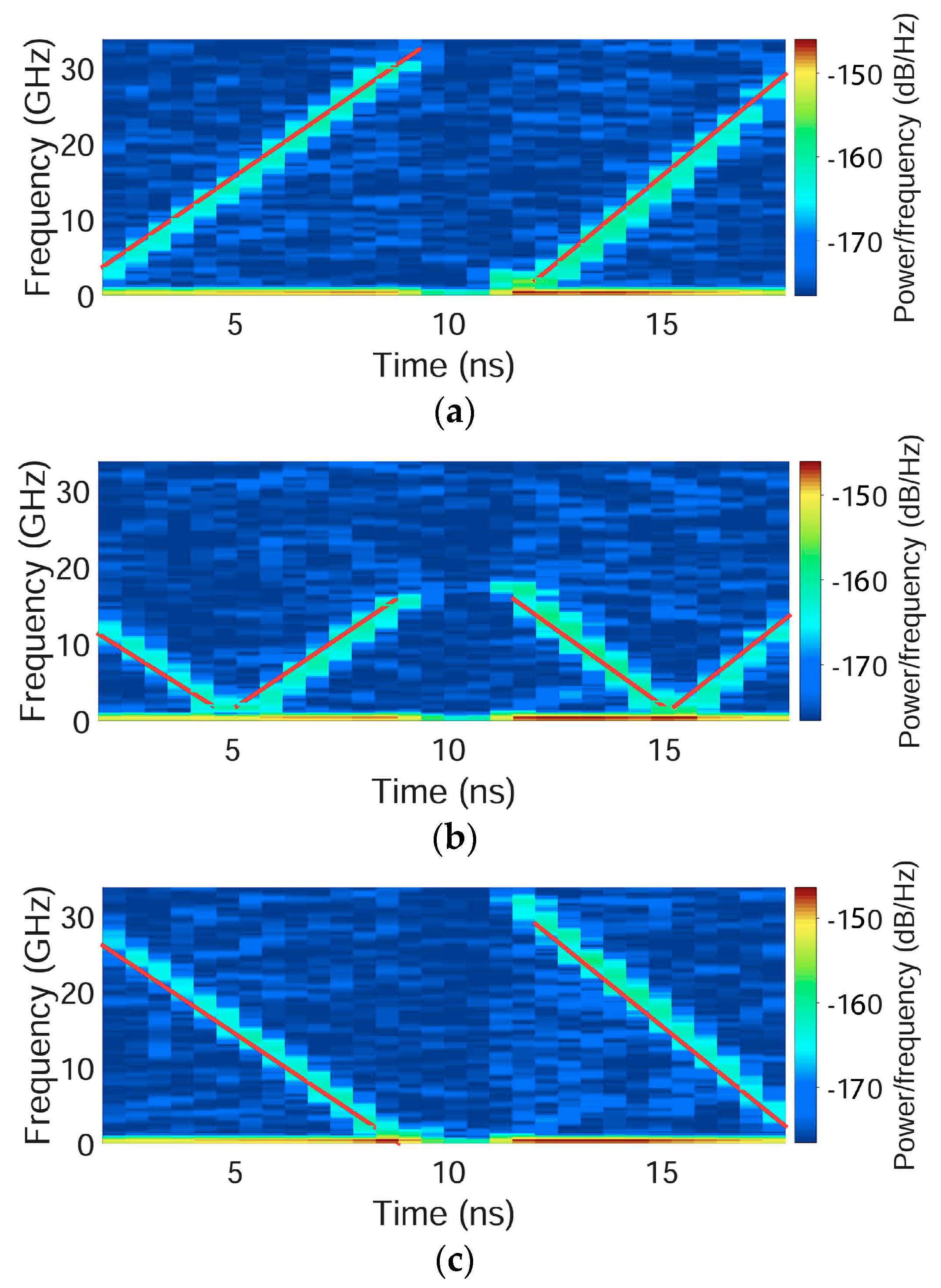
The characteristics of the generated waveforms are summarized in Figure 4, Figure 5 and Figure 6. Figure 4 shows the optical spectra and temporal waveforms for a delay time in the Sagnac interferometer of ∆t = −100 ps, 0 ps, and +100 ps (the difference in power between the two spectral bands and hence the two waveforms is due in part to the spectrum of the pulsed source and the setting of the EDFA used prior to detection). The two waveforms are separated temporally by 9.8 ns; this separation is determined by the product of the difference between the central wavelengths of the two spectral bands (5.7 nm) and the amount of dispersion (−1719 ps/nm). Since we use a negative dispersion element in our experiments, the WTM is reversed: while the spectra show the FSR varying in one direction, the temporal traces show the reverse. Moreover, the first (temporal) waveform (on the left) corresponds to longer wavelengths, whereas the second waveform (on the right) is associated with shorter wavelengths. Figure 5 shows the calculated spectrograms for these waveforms, which confirm simultaneous generation of two different chirped microwave waveforms. By tuning the delay, we can change the sign of the RF chirp rate as well as the central frequency (as explained previously, both waveforms have the same central frequency). Since the grating chirps are different, both waveforms exhibit different RF chirp rates. Finally, Figure 6 shows the RF spectra for the two waveforms. The waveforms occupy a frequency span of up to 26 GHz for delay times of ±100 ps and up to 19 GHz for a delay time of 0; these results are consistent with those shown in the spectrogram distributions. The full-width at half-maximum (FWHM) durations for the first and second waveforms are ~8.4 ns and ~7.0 ns, respectively; the corresponding time bandwidth products (TBWPs) are as large as 274 and 224.
2.3. Photonic Generation of Chirped Microwave Waveforms Using an Arrayed Waveguide Grating Sagnac Interferometer
The use of superimposed gratings in a Sagnac interferometer allows for the simultaneous generation of multiple chirped microwave waveforms using a simple structure with real-time tunability/reconfigurability. However, one main limitation of the approach is the fact that the generated waveforms have the same central frequency. Thus, while the Sagnac interferometer with superimposed gratings has the same functionality as multiple Sagnac interferometers with individual gratings, it cannot achieve the same capability for independent tuning of the waveform characteristics.
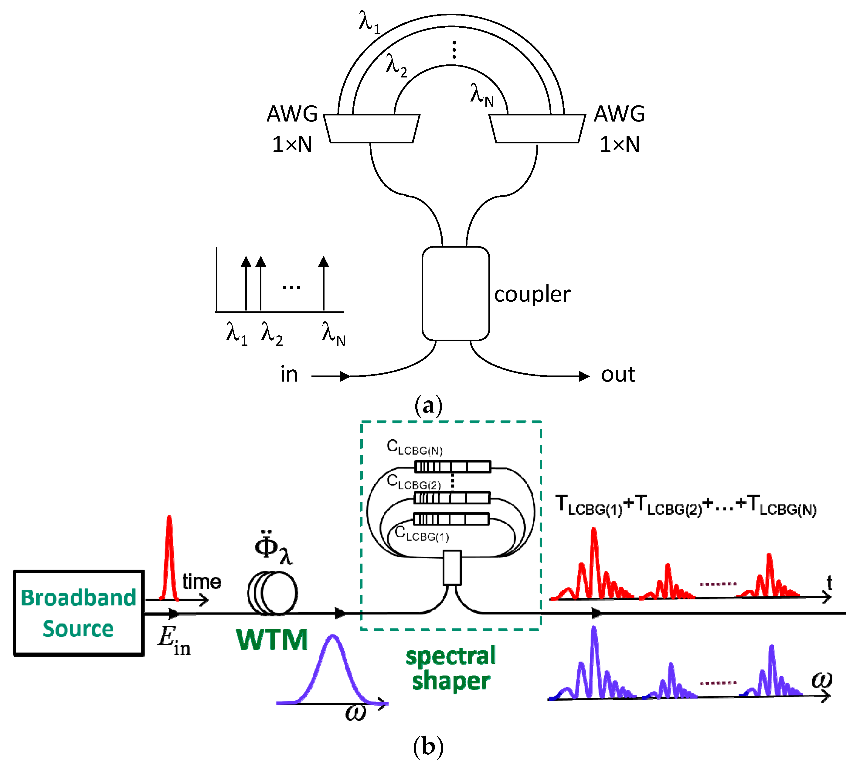
Capmany et al. demonstrated that it is possible to create a multi-channel (or multi-wavelength/multiple spectral bands) Sagnac interferometer using arrayed waveguide gratings (AWGs), i.e., an AWGSI (see Figure 7a) [32]. The AWGSI can also achieve the same functionality as multiple Sagnac interferometers, especially if we consider that each Sagnac interferometer operates over a specific spectral band. In each branch of the AWGSI (i.e., in each spectral band or channel), we can incorporate a linearly chirped BG as well as a tunable ODL (see Figure 7b). In so doing, we now have a Sagnac interferometer operating over multiple spectral bands where, in each, we have control over the characteristics by tuning the different ODLs [33]. Thus, each channel of the AWGSI can be used to generate a single chirped microwave waveform where the characteristics of the waveform, such as the sign and magnitude of the RF chirp rate and the central frequency, are determined by the characteristics of the linearly chirped BG and the delay time. In other words, we can generate simultaneously multiple chirped microwave waveforms where we can adjust the central frequency and RF chirp rate of each waveform independently and in real time.
As a proof-of-principle demonstration, we generate simultaneously two chirped microwave waveforms using a fiber-based two-channel AWGSI incorporating linearly chirped BGs. The experimental setup is shown in Figure 8 and is nominally the same as that shown in Figure 3, with the exception of the AWGSI replacing the Sagnac interferometer with superimposed gratings. To implement the two-channel AWGSI, we use 3 dB couplers and a pair of matched OBFs in each branch. The spectral widths of the two channels (set by the OBFs) are 1 nm and 0.7 nm. Each branch incorporates a linearly chirped BG having a reflectivity ~80%, center wavelength = 1540 nm, 3 dB bandwidth ~10 nm, and dispersion of ~140 ps/nm (i.e., gratings with the same characteristics are used). The OBFs in each branch are adjusted to occupy different spectral bands of the grating response; in this case, the bottom branch is set to cover shorter wavelengths while the top branch covers longer wavelengths. Each branch also has its own tunable ODL to control the path mismatch/delay time to allow for independent tuning of the central frequency and sign of the RF chirp rate.
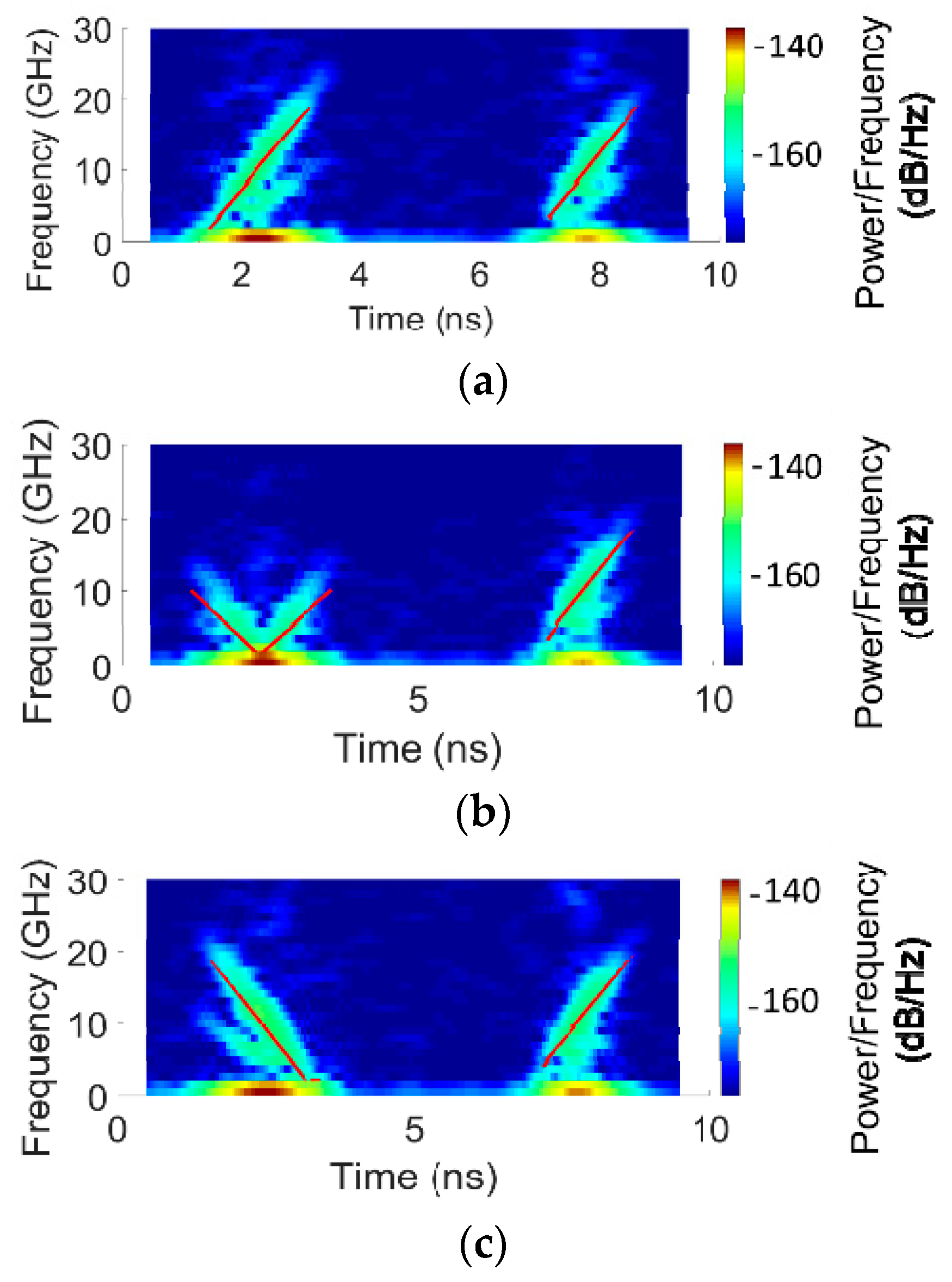
The characteristics of the generated waveforms are summarized in Figure 9, Figure 10 and Figure 11. In these experiments, we fix the path mismatch/delay time in the bottom branch (at shorter wavelengths) to ∆t = −70 ps and vary the delay in the top branch (at longer wavelengths). Figure 9 shows the optical spectra and temporal waveforms. Again, due to the use of a negative dispersion element, the WTM is reversed. The corresponding calculated spectrograms appear in Figure 10. Clearly, the characteristics of the first waveform (on the left and associated with longer wavelengths) vary while those of the second waveform (on the right and associated with shorter wavelengths) are held constant. This shows the ability of the AWGSI to provide independent tuning of the generated waveforms, a capability not possible with superimposed gratings.
Note that the magnitude of the RF chirp rate for both waveforms is the same, as the two gratings have nominally the same characteristics. It is possible to have different values of RF chirp rate if gratings with different chirp are used. Figure 11 illustrates the RF spectra for the two waveforms. The frequency spans a range of up to 24 GHz for delay times of ±70 ps and up to 16 GHz for a delay time of 0 ps. Given the difference in the spectral widths of the two channels, the durations of the waveforms are not the same: here, the first waveform has a FWHM of ~1.7 ns while that of the second waveform is ~1.2 ns. The waveforms are separated temporally by ~3.4 ns, which again is determined by the separation of the spectral bands and the dispersion. For a delay time of −70 ps, the TBWPs of the first and second waveforms are 29.5 and 14.4, respectively.
2.4. Discussion
We have demonstrated simultaneous generation of multiple (two) chirped microwave waveforms with using an optical spectral shaper based on (1) superimposed linearly chirped BGs in a Sagnac interferometer and (2) an AWGSI incorporating linearly chirped BGs in each branch. Both approaches can be scaled to generate a greater number of waveforms: for example, the superposition of at least nine fiber BGs was demonstrated [34] and AWGs operating over many wavelengths are readily available. While the use of superimposed gratings in a Sagnac interferometer offers greater simplicity in terms of implementation, it cannot provide the same capability as the AWGSI, especially in terms of generating waveforms with very different central frequencies. Moreover, by using tunable chirped BGs, e.g., through pump tuning [35], the AWGSI offers the possibility to generate multiple waveforms, with independent tuning of the central frequency and RF chirp rate.
Several factors will limit the number of waveforms that can be generated simultaneously. For example, in fiber, the number of gratings that can be superimposed depends on the photosensitivity of the fiber and the strength of each grating (which is set by corresponding peak refractive index change). Another factor is associated with the following. The repetition rate (R) of the mode-locked laser (or pulsed broadband source) used in the system gives a period (or temporal window) of 1/R into which the generated waveforms can be fit without interleaving. To first order, assuming that the generated waveforms have the same duration, the total number of waveforms is obtained by dividing the temporal window by the duration of a waveform. The duration of each waveform depends on the optical spectral bandwidth and the amount of dispersion used for WTM. These values are typically set by the need to have very large TBWP (e.g., to support a high compression ratio). As such, while the number of spectral bands can be high, the number of waveforms might be less.
Perhaps the greatest advantage of the AWGSI approach is the potential for integration, e.g., in SiP. In particular, high performance AWGs in SiP [36] have been realized and BGs are now routinely produced [37,38]. By introducing a pn junction to the silicon waveguide and applying a bias voltage, reconfiguration can be enabled through the plasma dispersion effect. In particular, if the junction is introduced along the rib waveguide BG, the grating chirp, and hence RF chirp rate, can be tuned [27]. On the other hand, using a pn junction for a silicon waveguide that is part of an interferometer branch will allow for tuning the path mismatch, and, hence, control over the central frequency. Such advances will result in the implementation of a fully programmable and integrated multiple chirped microwave waveform generator.
3. Photonic Radio-Frequency Spectrum Analysis
3.1. Context
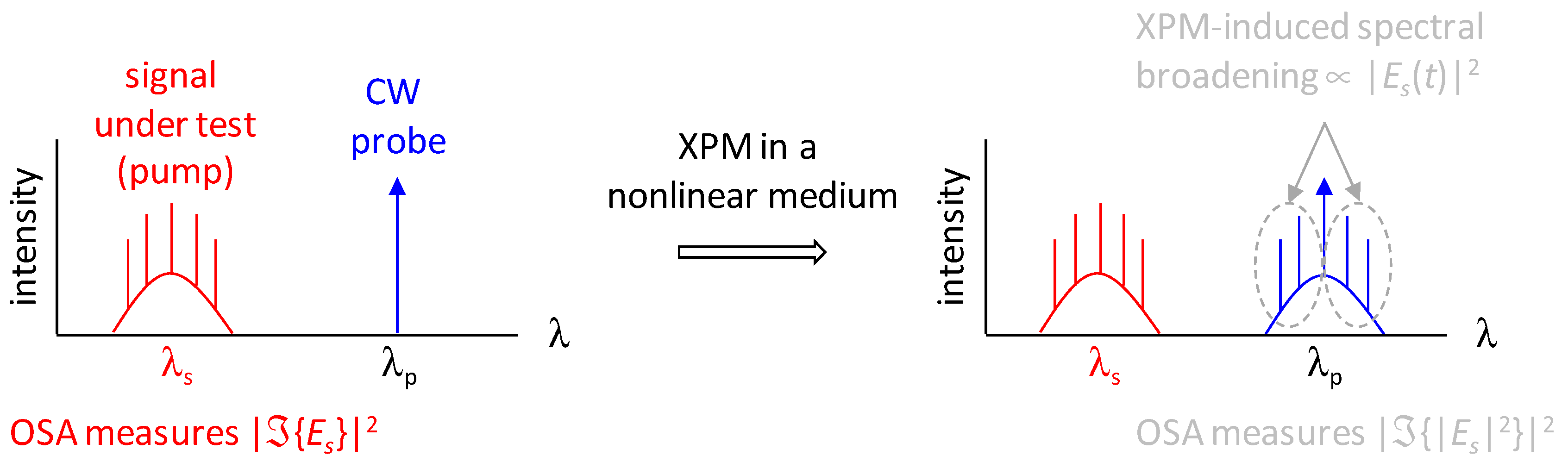
The RF spectrum of an optical signal under test, denoted Es(t), is given by the Fourier transform of its intensity . In fact, an ESA that is connected to a photodiode that detects Es(t) will display the squared magnitude of the Fourier transform of its intensity, i.e., . The principle for photonic RFSA is illustrated in Figure 12 and described in detail in [12]. Briefly, the signal under test (referred to as the ‘pump’) will phase modulate a continuous wave (CW) ‘probe’ via cross-phase modulation (XPM) in a nonlinear waveguide. For certain conditions, it can be shown that the XPM-induced sidebands on the probe, i.e., from phase modulation, are determined by the intensity of the signal under test. Thus, measuring the power spectral density around the probe using an optical spectrum analyzer (OSA) (which gives the squared magnitude of the Fourier transform of the field of the signal being measured) will correspond effectively to the RF spectrum of the signal under test, i.e., the OSA measurement gives .
The bandwidth for photonic RFSA can exceed several THz. The use of bidirectional propagation [39] and orthogonal polarizations [40] in a polarization maintaining highly nonlinear fiber can increase the number of optical signals that can be characterized using a single nonlinear waveguide medium to four. However, no further scaling in the number of signals that can be characterized is possible. Multi-channel simultaneous RFSA operation in a single integrated device will be beneficial as it can reduce footprint when compared to the duplication of single mode nonlinear waveguides. Moreover, such a multi-channel approach can still seek to exploit bidirectional propagation and orthogonal polarizations to gain a factor of four in terms of the number of signals (channels) that can be processed. Integrated waveguides can be engineered to support several propagating spatial modes. Each of the modes can then be used to process a different signal; as such, a single multimode waveguide can support parallel (simultaneous) multi-channel operation, i.e., spatial modes are utilized rather than a dedicated nonlinear waveguide per processed signal. For example, by harnessing nonlinear optics based on mode selectivity, Ding et al. demonstrated simultaneous four wave mixing (FWM)-based wavelength conversion of two wavelength channels [41] while we achieved simultaneous regenerative wavelength conversion of two wavelength channels using XPM [42]. Since photonic implementation of RFSA is based on XPM, we consider exploiting mode selective nonlinear optics to characterize simultaneously multiple ultrahigh repetition rate optical signals [43].
3.2. Integrated Mode-Selective Nonlinear Device
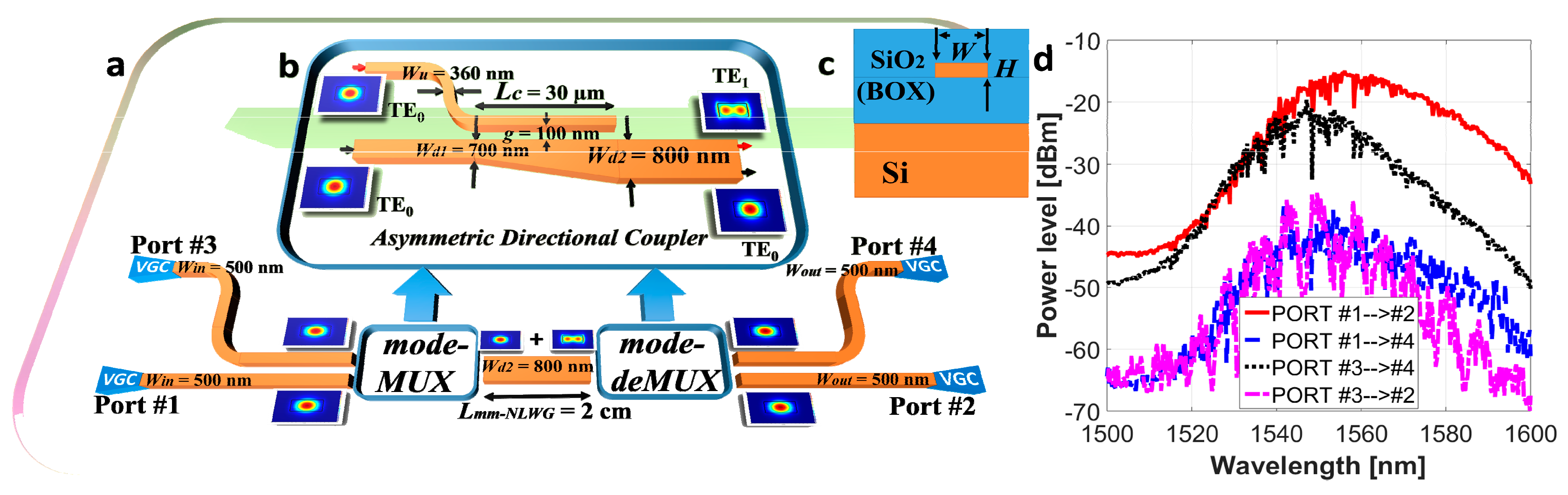
To demonstrate the principle of operation, we designed and fabricated an integrated (two channel) mode selective nonlinear device (MSND) in SiP as depicted in Figure 13. The MSND uses silicon waveguides that have a thickness H = 220 nm and sit on top of a 3 µm buried oxide (BOX) layer with a 2 µm thick index-matched top oxide cladding (the waveguide cross section appears in Figure 13c). It comprises the following: vertical grating couplers (VGCs) for input and output coupling to optical fiber, a multimode (here two modes) nonlinear waveguide (mm-NLWG), and a mode multiplexer and demultiplexer (m-MUX/m-deMUX) to convert single mode input from the fibers/VGCs to appropriate modes that propagate in the mm-NLWG and vice versa.
Figure 13b shows the design of the m-MUX and m-deMUX, which are based on asymmetric directional couplers (ADCs) [44,45]. The principle of operation is as follows. An optical signal that is launched into Port #3 will propagate as a transverse electric (TE0) or fundamental mode in the upper waveguide on the input side of the ADC and be converted to the TE1 mode on the output side. It then propagates as a TE1 mode in the mm-NLWG. On the other hand, an optical signal that is launched into Port #1, i.e., in the lower waveguide on the input side of the ADC will maintain its mode profile (TE0) at the ADC output and then propagate as a TE0 mode in the mm-NLWG. The width of the upper waveguide in the ADC is 360 nm while that of the lower waveguide extends linearly from 700 nm to 800 nm; this allows for phase matching between the TE0 and TE1 modes for mode transformation. The coupling gap and length of the ADCs are chosen to be 100 nm and 30 µm, respectively; this gives a coupling efficiency of up to 91% over a wavelength range of 100 nm from 1500 nm to 1600 nm.
The mm-NLWG has a width of 800 nm and supports the TE0 and TE1 modes as well as the first two transverse magnetic modes that are not excited due to the specific designs of the VGCs we used (which are optimized for TE mode operation). Table 1 summarizes the characteristics of the modes in the mm-NLWG.
In the MSND, we denote the transmission from Port #1 to Port #2 as Channel #1 and that from Port #3 to Port #4 as Channel #2. The measured intra-channel transmissions within Channel #1 or #2 and inter-channel transmission between Channel #1 and #2 are shown in Figure 13d. These measurements account for coupling loss (~6 dB/coupler) and propagation loss. The linear inter-channel cross-talk (i.e., either from Port #1 to #4 or from Port #3 to #2) is more than 15 dB less than the corresponding intra-channel cases.
Nonlinear optical effects (e.g., FWM or XPM) occur when both a high power pump and a CW probe propagate in the same mode in the mm-NLWG. In particular, if a high power pump and a CW probe are input at Port #1, they will propagate as a TE0 mode in the mm-NLWG (or equivalently, on Channel #1). Similarly, if the pump and CW probe are input at Port #3, they will propagate as a TE1 mode in the mm-NLWG (or on Channel #2). However, no nonlinear interactions occur if the pump and the CW probe are input on separate ports because they will propagate as different modes in the mm-NLWG and the inter-modal nonlinear interaction is very limited.
To characterize the nonlinear crosstalk, we compare the highest XPM-induced power around the probe when both pump and probe are input on the same channel (e.g., both are on Channel #1) to when they are launched on different channels (e.g., the pump is on Channel #2 whereas the probe is on Channel #1). Measurements show that the nonlinear inter-channel crosstalk at 1540 nm and 1560 nm is −30 dB. We can then infer the nonlinear coefficients for inter-modal interactions to be ~0.15 m−1·W−1 from the TE0 to TE1 modes and ~0.19 m−1·W−1 from the TE1 to TE0 modes.
3.3. Bandwidth Measurements
The maximum bandwidth for a photonic implementation of RFSA is given by [12]
where D is the dispersion and S the dispersion slope of the nonlinear waveguide (both at the central wavelength of the signal under test), and Δλ is the wavelength detuning between the CW probe and the signal. From the simulated dispersion properties of the mm-NLWG, the maximum theoretical bandwidths on Channel #1 and #2 are 4.5 THz and 1.5 THz, respectively, for a 10 nm detuning in a 2 cm long waveguide. This estimate does not account for higher order dispersion, which will reduce this bandwidth.
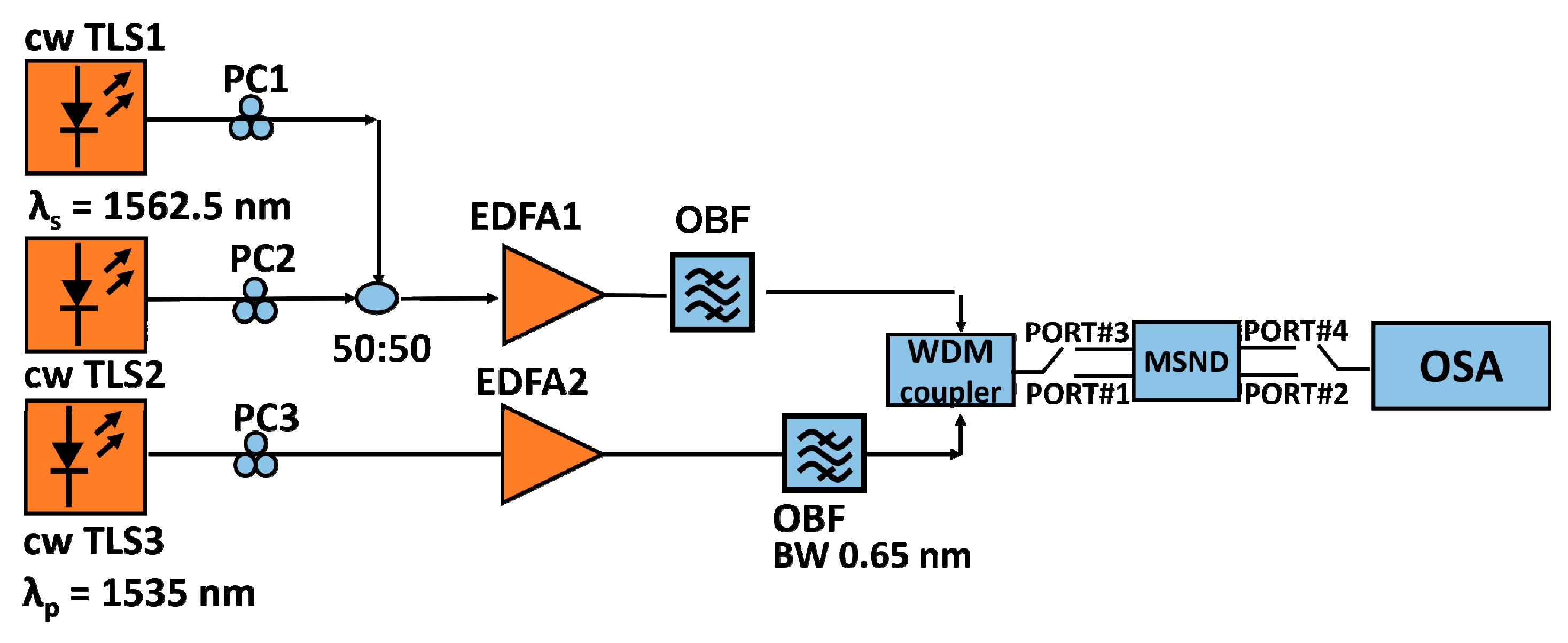
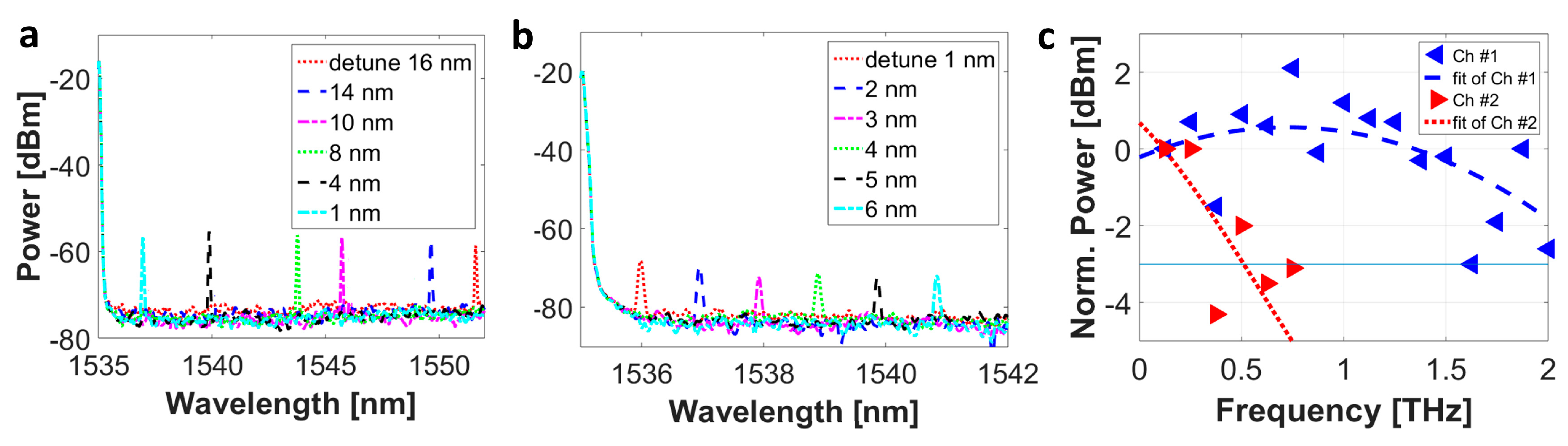
We measured the bandwidth of our RFSA using the setup illustrated in Figure 14. The pump (or signal under test) is the beat signal from two CW lasers whose wavelengths are located about λs = 1562.5 nm; the probe is a CW signal at λp = 1535 nm. λs and λp were chosen according to the spectral responses of the VCGs and the availability of optical filters and amplifiers. We adjusted the beat frequency (df) by detuning the two CW lasers symmetrically about λs. The bandwidth on each channel of the RFSA was then obtained by examining the variation in the power level of the XPM-induced sidebands at ±df from λp as a function of df (for these measurements, we used an OSA with 0.1 nm resolution bandwidth). To avoid nonlinear absorption in the mm-NLWG, we maintained the total power launched into Channel #1 to be 23.4 mW (the probe alone accounted for 8.9 mW) and into Channel #2 to 37.1 mW (the probe alone accounted for 15.1 mW). Figure 15a,b show the spectral evolution about λp as df is increased while 15c shows the response for both channels (the traces are based on a 2nd-order polynomial fit to the measured values). Note that, in Figure 15c, optical powers at higher frequencies are all normalized to the optical power at 0.125 THz (i.e., a wavelength detuning between the two CW pump signals of 1 nm). The fluctuations in the measured responses are due to the ripples in the spectral responses of the VGCs (e.g., the peak-to-peak ripple for a VGC-to-VCG test structure is 3.6 dB). The 3 dB bandwidths for Channel #1 and Channel #2 are >2.0 THz and 0.5 THz, respectively. With the chosen values of λs and λp, the XPM-induced spectral tones at ±df will overlap with the FWM idlers from the two beating CW signals for a detuning greater than 11 nm; this restricts the effective bandwidth of the MSND to 1.4 THz. The measured bandwidths are generally smaller than those estimated using Equation (5). The differences arise from (1) the fact that the calculated values only account for the dispersion and dispersion slope of the waveguide and not higher order values of dispersion and (2) limitations on measuring the output power of the beat signal due to ripples, the bandwidth, and the shape of the VGC spectral response.
3.4. Multi-Channel Results
We demonstrate simultaneous characterization of the RF spectrum for two ultrahigh repetition rate optical pulse trains, one at 160 GHz and the other at 640 GHz, using the setup in Figure 16. A mode-locked laser at 1550 nm and having a repetition rate of 10 GHz is first divided into two branches. In one branch, we use a commercial optical multiplexer (OMUX) to increase the repetition rate to 160 GHz. The OMUX is designed nominally to increase the data rate of a 27–1 pseudo-random bit sequence (PRBS), i.e., to obtain a 27–1 PRBS at 40 Gb/s, 80 Gb/s, or 160 Gb/s from a 27–1 PRBS at 10 Gb/s. In this sense, we do not have a true 160 GHz pulse train, i.e., the OMUX does not perform true pulse repetition rate multiplication. This can be verified by observing the optical spectrum of the 160 GHz pulse train, which exhibits 10 GHz spectral tones as opposed to only tones separated by 160 GHz. In the second branch, we filter two tones separated by 640 GHz to create a 640 GHz sinusoidal waveform by optical heterodyning. These two ultrahigh repetition rate (bandwidth) signals are amplified and filtered and used as separate pump signals before being combined with the CW probes using wavelength-division-multiplexing (WDM) couplers. The wavelengths of the CW probes launched into Channel #1 and Channel #2 are 1540 nm and 1559 nm, respectively. The average powers launched into the MSND are the following: 69.2 mW and 31.6 mW, respectively, for Channel #1, and 63.1 mW and 32.3 mW, respectively, for Channel #2. The estimated nonlinear phase shifts for both channels are ~0.12 radians which ensures accuracy for the extraction of the RF spectrum. At these power levels, we again observe negligible nonlinear absorption in the mm-NLWG. We measure the output spectra on each channel using the OCSA (with 0.16 pm or 20 MHz resolution), which provides more details on the photonic RF spectrum of the signals under test. Note that the scanning rate of photonic RFSA depends on that of the OSA used which, in turn, depends on settings such as sensitivity. Our measurements with the OCSA were obtained with a relatively high sensitivity (typically −70 dBm) and a sweep would take a few seconds.
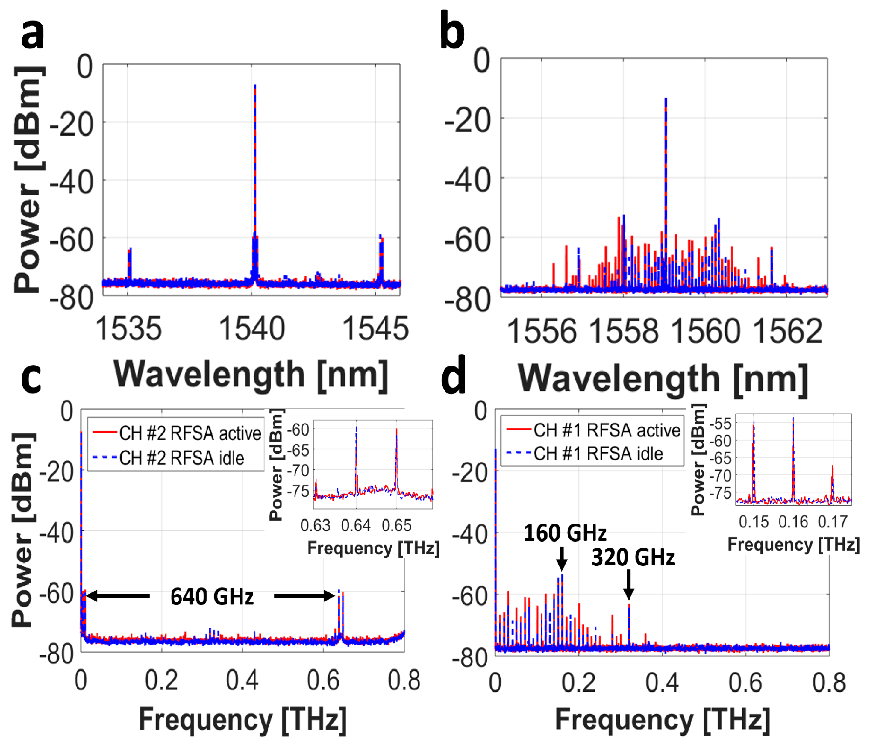
The results are summarized in Figure 17: Figure 17a,b show the optical spectra measured at the output for Channel #1 and #2, respectively, during simultaneous RFSA operation; Figure 17c,d highlight the corresponding RF spectra (i.e., half of the sideband measured from the probe wavelength). The red curves are obtained when both channels are active, i.e., for simultaneous characterization of the two signals, whereas the blue curves correspond to the case when only the observed channel is active. For Channel #1, a 640 GHz tone is detected properly. For Channel #2, the RF spectrum of the 160 GHz pulse train shows harmonics at 10 GHz; as explained previously, this is due to the fact that the multiplexer does not perform true pulse repetition rate multiplication. Nevertheless, we can identify a 160 GHz tone along with one at 320 GHz. We can see that the 640 GHz tone in Channel #1 is not impacted whether or not the signal in Channel #2 is active; more specifically, when Channel #2 is active, the 160 GHz spectral tone does not appear at the output of Channel #1. Similarly, the 640 GHz tone from the signal on Channel #1 does not appear in the spectral output of Channel #2. These results verify the fact that we can perform simultaneous RFSA for each channel in the MSND with negligible inter-channel interference.
3.5. Discussion
There are two primary factors that determine the number of channels that can be processed, i.e., the number of spatial modes that can be supported by the MSND: (1) the number of modes that can be multiplexed using the ADC and (2) the ability to obtain sufficient nonlinear optical effects in the higher order spatial modes. First, while it is possible to obtain phase matching so that the TE0 mode can be transformed to many higher order modes, the smaller difference in effective indices of the modes can induce greater inter-channel cross-talk during mode conversion. ADCs capable of exciting eight modes in a multi-mode waveguide (TE0–TE3 and TM0–TM3) have been realized [45]; however, scaling to a greater number of modes may require new and/or more complex m-MUX/m-deMUX designs. Second, the effective area of higher order modes is greater than for the fundamental and lower order modes. As such, the peak power required for higher order modes to achieve a similar nonlinear phase change for lower order modes will be greater. This can create problems in terms of nonlinear absorption, especially if SiP is considered for developing the MSND. In this context, a material platform such as silicon-rich nitride may be more suitable, as it does not show nonlinear absorption effects [46,47].
While the results shown in this paper focused on photonic RFSA of high repetition rate optical pulse trains, and, in particular, identification of the associated RF frequency tones, we can also monitor impairments such as the impact of dispersion on these pulse trains (see, e.g., [13,14,15,16,17,43]). Moreover, as demonstrated in [48], we can obtain the RF spectra of more arbitrary waveforms such as pulse bursts having uniform, apodized, and ramped envelopes/profiles and frequency content at 40 GHz and 80 GHz. Ultimately, a trade-off between bandwidth and resolution must be made; unless a high resolution OSA is used, the resolution might be limited even if very high bandwidth signals can be characterized.
4. Conclusions
In this review paper, we described approaches to generate simultaneously two chirped microwave waveforms as well as to perform simultaneous RFSA of two ultrahigh repetition rate optical pulse trains.
In terms of simultaneous generation of multiple chirped microwave waveforms, the AWGSI incorporating linearly chirped BGs achieves the same functionality and capability as having multiple Sagnac interferometers, each incorporating its own grating (regardless of whether a fiber-based or photonic integrated circuit based approach is considered). While both approaches use the same number of gratings, the AWGSI achieves its ‘parallel’ nature by exploiting the wavelength domain, which, in turn, reduces complexity and the number of components needed for its implementation. Parallel operation via the wavelength domain can also be applied to other spectral shaping techniques, such as the Fabry–Pérot cavity with distributed resonances.
Harnessing nonlinear optical effects in a mode selective manner represents another way to achieve parallel operation via spatial modes. In this paper, we considered RFSA based on XPM as the nonlinear optical effect. FWM is another nonlinear optical effect that has been used to perform IFM for microwave sensing applications [49,50,51]. Simultaneous wavelength conversion of two optical signals based on FWM has been demonstrated using the MSND [41]. As such, we can also expect to perform simultaneous IFM for at least two microwave signals. Moreover, as different nonlinear effects are excited in a mode selective manner, and as the inter-channel nonlinear effects are minimal, it should also be possible to realize multi-functional operation with the MSND, e.g., RFSA can be performed on one channel with IFM on the other. Such multi-channel and multi-functional microwave signal processing can only be enabled through photonics. While scaling the number of channels that can be processed will be constrained by (1) the number of spatial modes that can be multiplexed/demultiplexed and (2) the nonlinear coefficient associated with the higher order modes (effectively, the amount of power required to obtain a sufficient nonlinear interaction), we can nonetheless take advantage of bidirectional propagation and orthogonal polarizations to increase by a factor of four the number of channels that can be processed via different spatial modes.
The most direct approach for multi-channel microwave photonic signal processing is to duplicate the processing block that performs the processing function, i.e., there will be as many processing blocks as there are channels to be processed. While this form of ‘parallel’ processing can indeed be implemented readily, it may not result in the most practical realization. This, in turn, may impose limits on scalability. The solutions and approaches presented in this paper demonstrate how simple ‘tricks’ can be used to process multiple signals simultaneously without the need for ‘brute force’ duplication and should stimulate further work on the topic.
Acknowledgments
This funding was supported in part by the Natural Sciences and Engineering Research Council of Canada (NSERC) CREATE NGON, NSERC CREATE Si-EPIC, and the Fonds de Recherche du-Nature et Technologies (FRQNT). The silicon photonic devices were fabricated by Richard Bojko at the University of Washington Nanofabrication Facility, a member of the National Science Foundation National Nanotechnology Infrastructure Network. We also thank Prof. Martin Rochette, Marwan Chehade, and Muhammad Anees of McGill University for their contributions to experimental work.
Author Contributions
L.R.C. conceived the ideas and supervised the work. P.M., M.M. and R.A. performed the experiments. M.M. designed the integrated silicon photonics device. All authors contributed to data analysis and manuscript writing.
Conflicts of Interest
The authors declare no conflict of interest.
References
- Capmany, J.; Novak, D. Microwave photonics combines two worlds. Nat. Photonics 2007, 1, 319–330. [Google Scholar] [CrossRef]
- Yao, J.P. Microwave photonics. IEEE/OSA J. Lightw. Technol. 2009, 27, 314–335. [Google Scholar] [CrossRef]
- Iezekiel, S.; Burla, M.; Klamkin, J.; Marpaung, D.; Capmany, J. RF engineering meets optoelectronics. IEEE Microw. Mag. 2015, 16, 28–45. [Google Scholar] [CrossRef]
- Yao, J.P. Photonic generation of microwave arbitrary waveforms. Opt. Commun. 2011, 284, 3723–3736. [Google Scholar] [CrossRef]
- Rashidinejad, A.; Li, Y.; Weiner, A.M. Recent Advances in Programmable Photonic-Assisted Ultrabroadband Radio-Frequency Arbitrary Waveform Generation. IEEE J. Quantum Electron. 2016, 52, 1–17. [Google Scholar] [CrossRef] [Green Version]
- Capmany, J.; Mora, J.; Gasulla, I.; Sancho, J.; Lloret, J.; Sales, S. Microwave photonic signal processing. IEEE/OSA J. Lightw. Technol. 2013, 31, 571–586. [Google Scholar] [CrossRef]
- Minasian, R.A.; Chan, E.W.H.; Yi, X. Microwave photonic signal processing. Opt. Express 2013, 21, 22918–22936. [Google Scholar] [CrossRef] [PubMed]
- Ng, W. Photonics for microwave systems and ultra-wideband signal processing. Opt. Commun. 2016, 373, 2–15. [Google Scholar] [CrossRef]
- Jiang, H.; Marpaung, D.; Pagani, M.; Vu, K.; Choi, D.-Y.; Madden, S.J.; Yan, L.; Eggleton, B.J. Wide-range, high-precision multiple microwave frequency measurement using a chip-based photonic Brillouin filter. Optica 2016, 3, 30–34. [Google Scholar] [CrossRef]
- Pan, S.; Yao, J.P. Photonics-based broadband microwave measurement. IEEE/OSA J. Lightw. Technol. 2017, 35, 3498–3513. [Google Scholar] [CrossRef]
- Zmuda, H.; Toughlian, E.N. Photonic Aspects of Modern Radar; Artech House: Norwood, MA, USA, 1994. [Google Scholar]
- Dorrer, C.; Maywar, D.N. RF Spectrum Analysis of Optical Signals Using Nonlinear Optics. J. Light. Technol. 2004, 22, 266–274. [Google Scholar] [CrossRef]
- Pelusi, M.; Luan, F.; Vo, T.D.; Lamont, M.R.E.; Madden, S.J.; Bulla, D.A.; Choi, D.-Y.; Luther-Davies, B.; Eggleton, B.J. Photonic-chip-based radio-frequency spectrum analyser with terahertz bandwidth. Nat. Photonics 2009, 3, 139–143. [Google Scholar] [CrossRef]
- Vo, T.D.; Pelusi, M.D.; Schröder, J.; Luan, F.; Madden, S.J.; Choi, D.Y.; Bulla, D.A.P.; Luther-Davies, B.; Eggleton, B.J. Simultaneous multi-impairment monitoring of 640 Gb/s signals using photonic chip based RF spectrum analyzer. Opt. Express 2010, 18, 3938–3945. [Google Scholar] [CrossRef] [PubMed]
- Corcoran, B.; Vo, T.D.; Pelusi, M.D.; Monat, C.; Xu, D.-X.; Densmore, A.; Ma, R.; Janz, S.; Moss, D.J.; Eggleton, B.J. Silicon nanowire based radio-frequency spectrum analyzer. Opt. Express 2010, 18, 20190–20200. [Google Scholar] [CrossRef] [PubMed]
- Vo, T.D.; Corcoran, B.; Schroder, J.; Pelusi, M.D.; Xu, D.X.; Densmore, A.; Ma, R.; Janz, S.; Moss, D.J.; Eggleton, B.J. Silicon-chip-based real-time dispersion monitoring for 640 Gbit/s DPSK signals. IEEE/OSA J. Lightw. Technol. 2011, 29, 1790–1796. [Google Scholar] [CrossRef]
- Ferrera, M.; Reimer, C.; Pasquazi, A.; Peccianti, M.; Clerici, M.; Caspani, L.; Chu, S.T.; Little, B.E.; Morandotti, R.; Moss, D.J. CMOS compatible integrated all-optical radio frequency spectrum analyzer. Opt. Express 2014, 22, 21488–21498. [Google Scholar] [CrossRef] [PubMed]
- Weiner, A.M. Optical pulse shaping: A tutorial review. Opt. Commun. 2011, 284, 3669–3692. [Google Scholar] [CrossRef]
- Chen, L.R. Photonic generation of chirped microwave and millimeter wave pulses based on optical spectral shaping and wavelength-to-time mapping in silicon photonics. Opt. Commun. 2016, 373, 70–81. [Google Scholar] [CrossRef]
- Wang, C.; Yao, J.P. Photonic generation of chirped millimeter-wave pulses based on nonlinear frequency-to-time mapping in a nonlinearly chirped fiber Bragg grating. IEEE Trans. Microw. Theory Tech. 2008, 56, 542–553. [Google Scholar] [CrossRef]
- Chi, H.; Yao, J.P. Chirped RF pulse generation based on optical spectral shaping and wavelength-to-time mapping using a nonlinearly chirped fiber Bragg grating. IEEE/OSA J. Lightw. Technol. 2008, 26, 1282–1287. [Google Scholar] [CrossRef]
- Wang, C.; Yao, J.P. Simultaneous optical spectral shaping and wavelength-to-time mapping for photonic microwave arbitrary waveform generation. IEEE Photonics Technol. Lett. 2009, 21, 793–795. [Google Scholar] [CrossRef]
- Spasojevic, M.; Chen, L.R. Discretely tunable optical delay lines using serial and step-chirped sidewall Bragg gratings in SOI. Electron. Lett. 2013, 49, 608–610. [Google Scholar] [CrossRef]
- Wang, C.; Yao, J.P. Photonic generation of chirped microwave pulses using superimposed chirped fiber Bragg gratings. IEEE Photonics Technol. Lett. 2008, 20, 882–884. [Google Scholar] [CrossRef]
- Ma, M.; Rochette, M.; Chen, L.R. Generating chirped microwave pulses using an integrated distributed Fabry–Pérot cavity in silicon-on-insulator. IEEE Photonics J. 2015, 7, 5500706. [Google Scholar] [CrossRef]
- Zhang, W.; Yao, J.P. Photonic generation of linearly chirped microwave waveforms using a silicon-based on-chip spectral shaper incorporating two linearly chirped waveguide Bragg gratings. IEEE/OSA J. Lightw. Technol. 2015, 33, 5047–5054. [Google Scholar] [CrossRef]
- Zhang, W.; Yao, J.P. Silicon-based on-chip electrically-tunable spectral shaper for continuous tunable linearly chirped microwave waveform generation. IEEE/OSA J. Lightw. Technol. 2016, 34, 4644–4672. [Google Scholar] [CrossRef]
- Wang, C.; Yao, J. Chirped microwave pulse generation based on optical spectral shaping and wavelength-to-time mapping using a Sagnac loop mirror incorporating a chirped fiber Bragg grating. IEEE/OSA J. Lightw. Technol. 2009, 27, 3336–3341. [Google Scholar] [CrossRef]
- Wang, J.; Ashrafi, R.; Rochette, M.; Chen, L.R. Chirped microwave pulse generation using an integrated silicon photonic spectral shaper. IEEE Photonics Technol. Lett. 2015, 27, 1876–1879. [Google Scholar] [CrossRef]
- Shu, X.; Yu, L.; Zhao, D.; Zhang, L.; Sugden, K.; Bennion, I. Transmission characteristics of Sagnac interferometers based on fiber Bragg gratings. J. Opt. Soc. Am. B 2002, 19, 2770–2780. [Google Scholar] [CrossRef]
- Moslemi, P.; Chen, L.R. Simultaneously generating multiple chirped microwave pulses with superimposed FBGs. IEEE Photonics Technol. Lett. 2017, 29, 1387–1390. [Google Scholar] [CrossRef]
- Capmany, J.; Muñoz, P.; Sales, S.; Pastor, D.; Ortega, B.; Martinez, A. Arrayed waveguide Sagnac interferometer. Opt. Lett. 2003, 28, 197–199. [Google Scholar] [CrossRef] [PubMed]
- Moslemi, P.; Chen, L.R.; Rochette, M. Simultaneously generating multiple chirped microwave waveforms using an arrayed waveguide Sagnac interferometer. IET Electron. Lett. 2017, 53, 1534–1535. [Google Scholar] [CrossRef]
- Bolger, J.A.; Littler, I.C.M.; Eggleton, B.J. Optimization of superimposed chirped fiber Bragg gratings for the generation of ultra-high speed optical pulse trains. Opt. Commun. 2007, 271, 524–531. [Google Scholar] [CrossRef]
- Shahoei, H.; Li, M.; Yao, J. Continuously tunable time delay using an optically pumped linear chirped fiber Bragg grating. IEEE/OSA J. Lightw. Technol. 2011, 29, 1465–1472. [Google Scholar] [CrossRef]
- Cheung, S.; Su, T.; Okamoto, K.; Yoo, S.J.B. Ultra-compact silicon photonic 512 × 512 25 GHz arrayed waveguide grating router. IEEE J. Sel. Top. Quantum Electron. 2014, 20, 8202207. [Google Scholar] [CrossRef]
- Burla, M.; Cortés, L.R.; Li, M.; Wang, X.; Chrostowski, L.; Azaña, J. Integrated waveguide Bragg gratings for microwave photonics signal processing. Opt. Express 2013, 21, 25120–25147. [Google Scholar] [CrossRef] [PubMed]
- LaRochelle, S.; Simard, A.D. Silicon photonic Bragg grating devices. In Proceedings of the Conference on Optical Fiber Communication, Los Angeles, CA, USA, 19–23 March 2017. [Google Scholar]
- Provost, L.; Parmigiani, F.; Petropoulos, P.; Richardson, D.J. Investigation of simultaneous 2R regeneration of two 40-Gb/s channels in a single optical fiber. IEEE Photonics Technol. Lett. 2008, 20, 270–272. [Google Scholar] [CrossRef]
- Provost, L.; Parmigiani, F.; Petropoulos, P.; Richardson, D.J.; Mukasa, K.; Takahashi, M.; Hiroishi, J.; Tadakuma, M. Investigation of four-wavelength regenerator using polarization- and direction-multiplexing. IEEE Photonics Technol. Lett. 2008, 20, 1676–1678. [Google Scholar] [CrossRef]
- Ding, Y.; Xu, J.; Ou, H.; Peucheret, C. Mode-selective wavelength conversion based on four-wave mixing in a multimode silicon waveguide. Opt. Express 2014, 22, 127–135. [Google Scholar] [CrossRef] [PubMed]
- Ma, M.; Chen, L.R. Harnessing mode-selective nonlinear optics for on-chip multi-channel all-optical signal processing. APL Photonics 2016, 1, 086104. [Google Scholar] [CrossRef]
- Ma, M.; Adams, R.; Chen, L.R. Integrated photonic chip enabled simultaneous multi-channel ultra-wideband radio frequency spectrum analyzer. IEEE/OSA J. Lightw. Technol. 2017, 35, 2622–2628. [Google Scholar] [CrossRef]
- Ding, Y.; Xu, J.; Da Ros, F.; Huang, B.; Ou, H.; Peucheret, C. On-chip two-mode division multiplexing using tapered directional coupler-based mode multiplexer and demultiplexer. Opt. Express 2013, 21, 10376–10382. [Google Scholar] [CrossRef] [PubMed]
- Wang, J.; He, S.; Dai, D. On-chip silicon 8-channel hybrid (de)multiplexer enabling simultaneous mode- and polarization-division-multiplexing. Laser Photonics Rev. 2014, 8, L18–L22. [Google Scholar] [CrossRef]
- Krückel, C.J.; Fülöp, A.; Klintberg, T.; Bengtsson, J.; Andrekson, P.A.; Torres-Company, V. Linear and nonlinear characterization of low-stress high confinement silicon-rich nitride waveguides. Opt. Express 2015, 23, 25827–25837. [Google Scholar] [CrossRef] [PubMed]
- Rezagholipour Dizaji, M.; Krückel, C.J.; Fülöp, A.; Andrekson, P.A.; Torres-Company, V.; Chen, L.R. Silicon-rich nitride waveguides for ultra-broadband nonlinear signal processing. Opt. Express 2017, 25, 12100–12108. [Google Scholar] [CrossRef] [PubMed]
- Samadi, P.; Chen, L.R.; Callender, C.L.; Dumais, P.; Jacob, S.; Celo, D. RF arbitrary waveform generation using tunable planar lightwave circuits. Opt. Commun. 2011, 284, 3737–3741. [Google Scholar] [CrossRef]
- Bui, L.A.; Pelusi, M.D.; Vo, T.D.; Sarkhosh, N.; Emami, H.; Eggleton, B.J.; Mitchell, A. Instantaneous frequency measurement system using optical mixing in highly nonlinear fiber. Opt. Express 2009, 17, 22983–22991. [Google Scholar] [CrossRef] [PubMed]
- Pagani, M.; Morrison, B.; Zhang, Y.; Casas-Bedoya, A.; Aalto, T.; Harjanne, M.; Kapulainen, M.; Eggleton, B.J.; Marpaung, D. Low-error and broadband microwave frequency measurement in a silicon chip. Optica 2015, 2, 751–756. [Google Scholar] [CrossRef]
- Pagani, M.; Vu, K.; Choi, D.-Y.; Madden, S.J.; Eggleton, B.J.; Marpaung, D. Instantaneous microwave frequency measurement using four-wave mixing in a chalcogenide chip. Opt. Commun. 2016, 373, 100–104. [Google Scholar] [CrossRef]
Figure 1.
Principle of (a) photonic generation of arbitrary microwave waveforms based on optical pulse shaping and optical-to-electrical (O/E) conversion and (b) generation of chirped microwave waveforms based on optical spectral shaping and wavelength-to-time mapping (WTM).
Figure 1.
Principle of (a) photonic generation of arbitrary microwave waveforms based on optical pulse shaping and optical-to-electrical (O/E) conversion and (b) generation of chirped microwave waveforms based on optical spectral shaping and wavelength-to-time mapping (WTM).
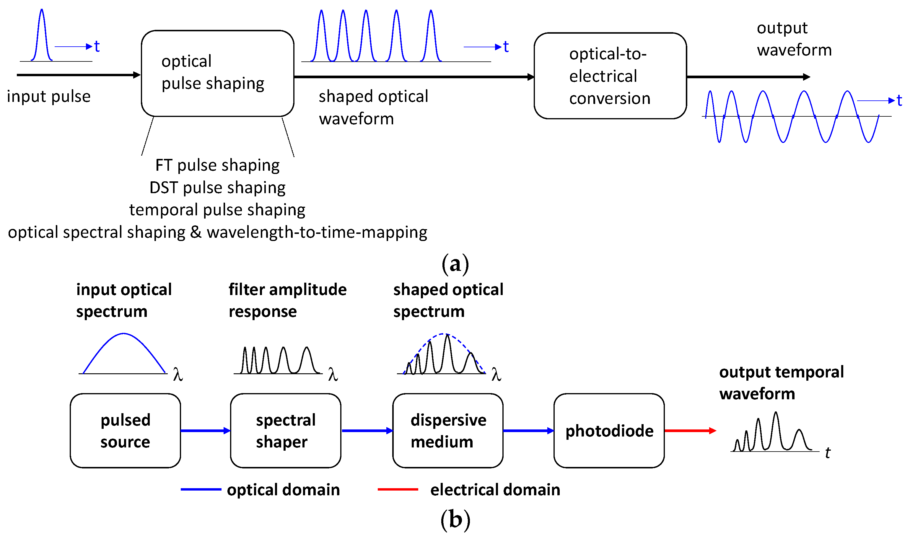
Figure 2.
(a) Spectral shaper based on a Sagnac interferometer incorporating a single linearly chirped Bragg grating (BG). Schematic of the system generating two (or multiple) chirped microwave pulses simultaneously with (b) multiple Sagnac interferometers each containing a linearly chirped BG and (c) a single Sagnac interferometer containing superimposed linearly chirped BGs. TLCBG(i) denotes the spectral response of the i-th Sagnac interferometer.


Figure 3.
Experimental setup for simultaneous generation of multiple chirped microwave waveforms using a Sagnac interferometer incorporating superimposed linearly chirped BGs.
Figure 3.
Experimental setup for simultaneous generation of multiple chirped microwave waveforms using a Sagnac interferometer incorporating superimposed linearly chirped BGs.

Figure 4.
Spectral and temporal results for delay times of −100 ps (a,b); 0 ps (c,d); and 100 ps (e,f).
Figure 4.
Spectral and temporal results for delay times of −100 ps (a,b); 0 ps (c,d); and 100 ps (e,f).

Figure 5.
Spectrogram distributions for the waveforms shown in Figure 4: delay times of (a) −100 ps; (b) 0 ps; and (c) 100 ps.
Figure 5.
Spectrogram distributions for the waveforms shown in Figure 4: delay times of (a) −100 ps; (b) 0 ps; and (c) 100 ps.

Figure 6.
Radio-frequency (RF) spectra for the two generated waveforms at longer wavelengths (left) and shorter wavelengths (right) for different delay times.
Figure 6.
Radio-frequency (RF) spectra for the two generated waveforms at longer wavelengths (left) and shorter wavelengths (right) for different delay times.
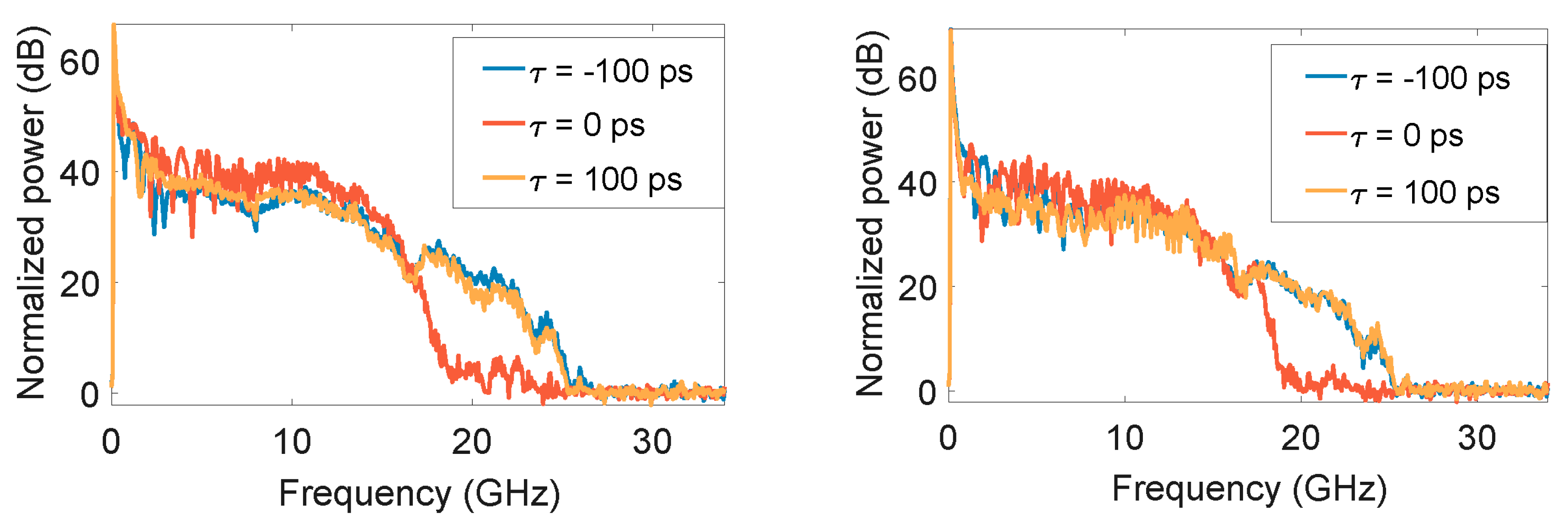
Figure 7.
(a) Schematic of an arrayed waveguide Sagnac interferometer (AWGSI) (adapted from [32]) and (b) its use for simultaneously generating multiple chirped microwave waveforms.
Figure 7.
(a) Schematic of an arrayed waveguide Sagnac interferometer (AWGSI) (adapted from [32]) and (b) its use for simultaneously generating multiple chirped microwave waveforms.

Figure 8.
Schematic of experimental setup for simultaneous generation of two chirped microwave waveforms using AWGSI incorporating linearly chirped BGs.
Figure 8.
Schematic of experimental setup for simultaneous generation of two chirped microwave waveforms using AWGSI incorporating linearly chirped BGs.
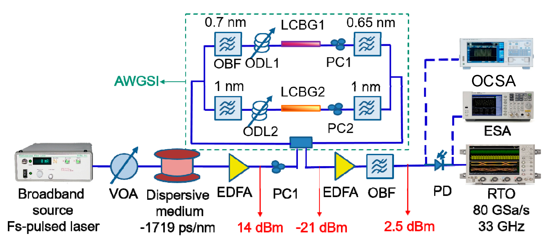
Figure 9.
Spectral and temporal results. The delay time in the bottom branch at shorter wavelengths is fixed at −70 ps while that in the top branch at longer wavelengths is varied: −70 ps (a,b); 0 ps (c,d); and +70 ps (e,f).
Figure 9.
Spectral and temporal results. The delay time in the bottom branch at shorter wavelengths is fixed at −70 ps while that in the top branch at longer wavelengths is varied: −70 ps (a,b); 0 ps (c,d); and +70 ps (e,f).
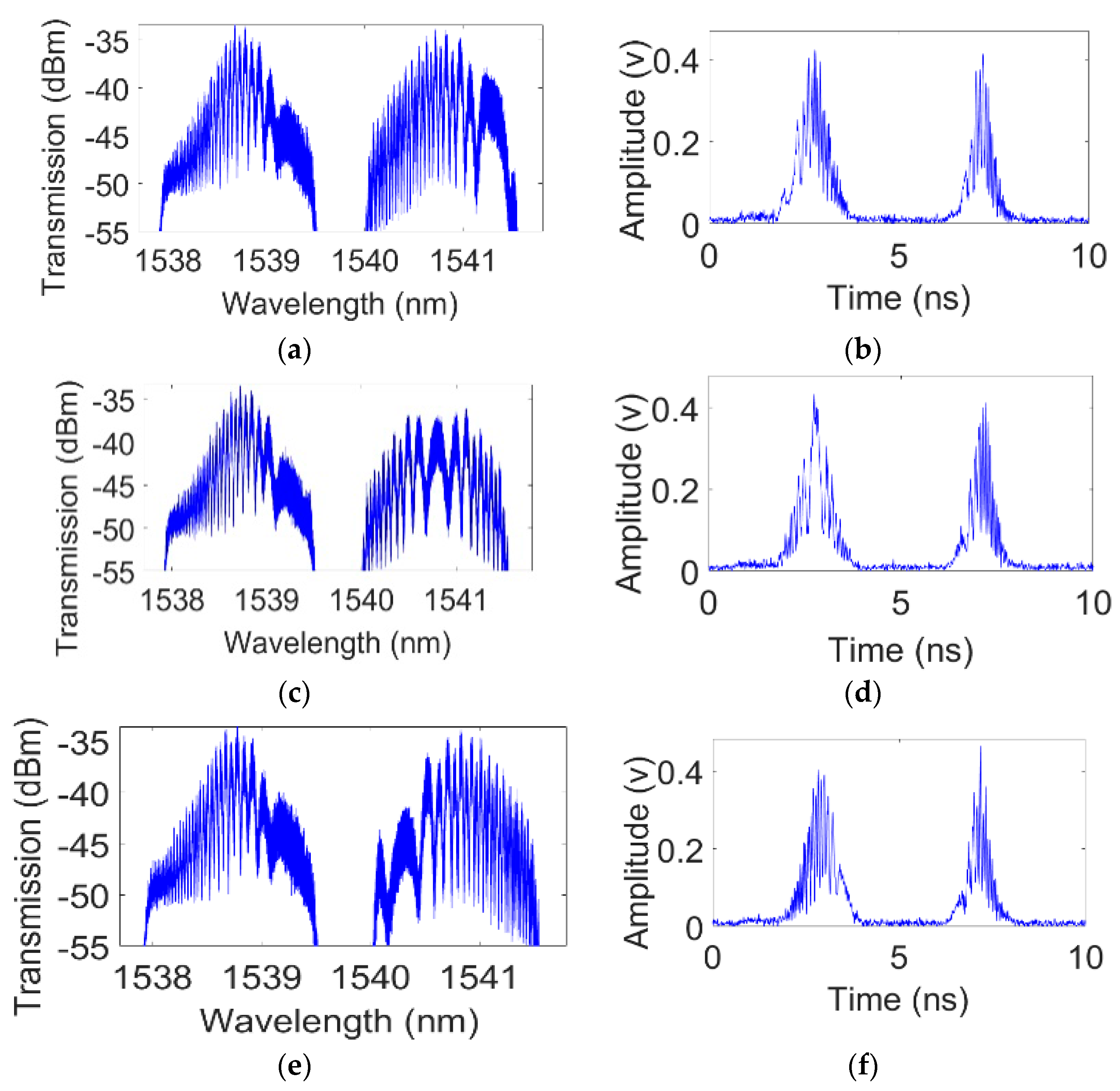
Figure 10.
Spectrogram distributions for the waveforms shown in Figure 9: delay times of (a) −70 ps; (b) 0 ps; and (c) 70 ps.
Figure 10.
Spectrogram distributions for the waveforms shown in Figure 9: delay times of (a) −70 ps; (b) 0 ps; and (c) 70 ps.

Figure 11.
RF spectra for the first generated waveform (left) and the second generated waveform (right) for different values of delay (the same delay is applied to both branches).
Figure 11.
RF spectra for the first generated waveform (left) and the second generated waveform (right) for different values of delay (the same delay is applied to both branches).
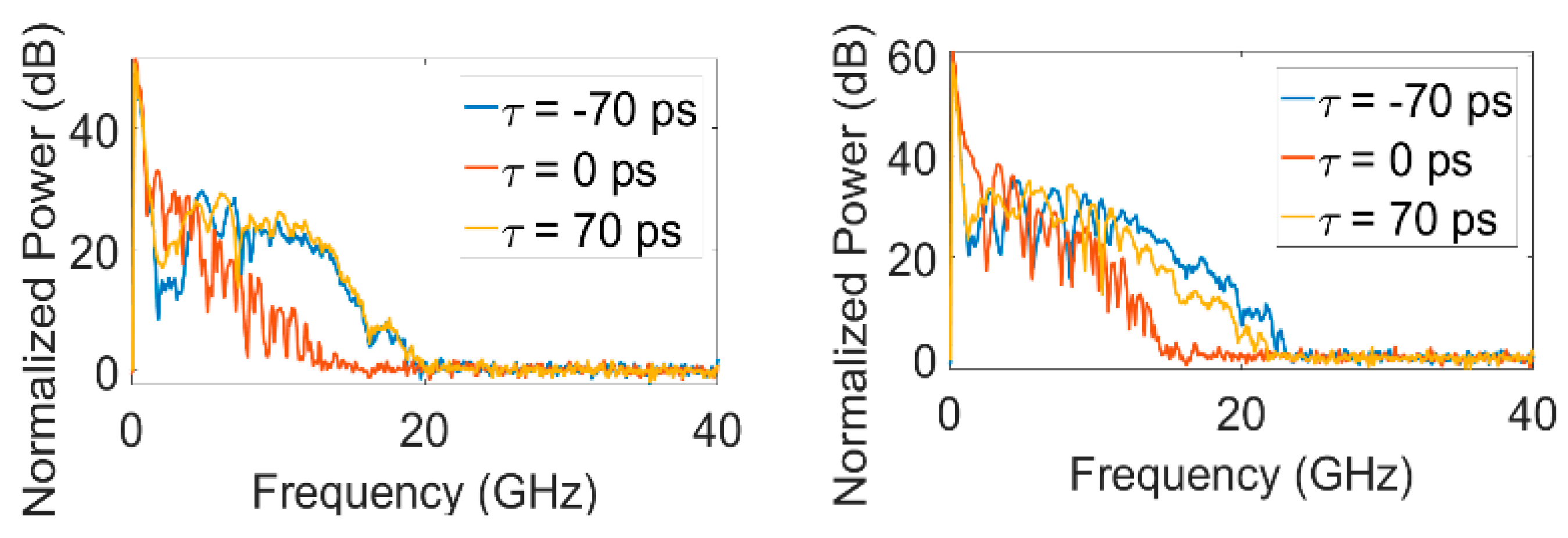
Figure 12.
Principle for photonic radio-frequency spectrum analysis (RFSA) (adapted from [13]).
Figure 12.
Principle for photonic radio-frequency spectrum analysis (RFSA) (adapted from [13]).

Figure 13.
(a) Schematic of mode selective nonlinear device (MSND) comprising vertical grating couplers (VGCs), mode multiplexer and demultiplexer (m-MUX/m-deMUX), and multimode nonlinear waveguide (mm-NLWG); (b) asymmetric directional couplers (ADC) structure; (c) cross section of silicon waveguide; (d) intra-channel and inter-channel transmittance (i.e., linear inter-channel cross-talk) over the wavelength span from 1500 to 1600 nm.

Figure 14.
Experimental setup for measuring the RFSA bandwidth.

Figure 15.
Evolution of the output spectrum from the MSND as the pump detuning increases for (a) Channel #1 and (b) Channel #2; (c) variation in output power of the XPM-induced tone as a function of df from which the bandwidth of the photonic RFSA is estimated.
Figure 15.
Evolution of the output spectrum from the MSND as the pump detuning increases for (a) Channel #1 and (b) Channel #2; (c) variation in output power of the XPM-induced tone as a function of df from which the bandwidth of the photonic RFSA is estimated.

Figure 16.
Experimental setup for multi-channel RFSA with a 640 GHz waveform on Channel #1 and a pulse train with a 160 GHz repetition rate on Channel #2. WSS: Finisar waveshaper.
Figure 16.
Experimental setup for multi-channel RFSA with a 640 GHz waveform on Channel #1 and a pulse train with a 160 GHz repetition rate on Channel #2. WSS: Finisar waveshaper.
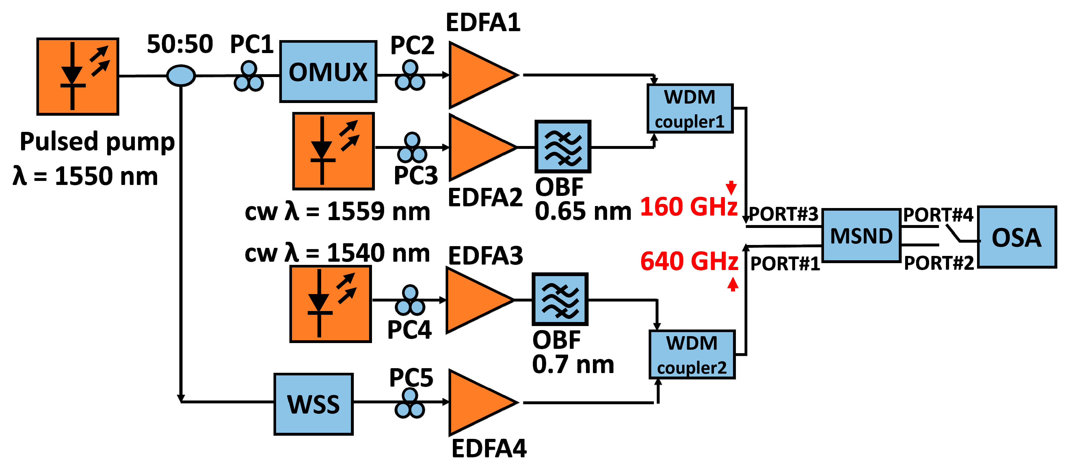
Figure 17.
Simultaneous multi-channel RFSA when the probe wavelengths are separated by 19 nm. XPM-induced sidebands are observed on (a) Channel #1 and (b) Channel #2; the half sideband RF spectrum is illustrated in (c) for Channel #1 and (d) for Channel #2. Insets: enlarged spectra around the 640 GHz and 160 GHz tones. The resolutions of the RF spectra shown are set by the resolution of the optical complex spectrum analyzer (OCSA); in this case, 20 MHz.

Table 1.
Characteristics of the TE modes in the multimode nonlinear waveguide (mm-NLWG) calculated using Mode Solver from Lumerical MODE Solutions and using a nonlinear index n2 = 4.5 × 10⁻¹⁸ m2/W.
Table 1.
Characteristics of the TE modes in the multimode nonlinear waveguide (mm-NLWG) calculated using Mode Solver from Lumerical MODE Solutions and using a nonlinear index n2 = 4.5 × 10⁻¹⁸ m2/W.
| Parameter | TE0 Mode | TE1 Mode |
|---|---|---|
| Dispersion @ 1550 nm, ps/(nm·cm) | −5.55 × 10⁻⁴ | 1.56 × 10⁻³ |
| Dispersion slope @ 1550 nm, ps/(nm·cm2) | 1.75 × 10⁻⁶ | −1.51 × 10⁻⁵ |
| Effective area, µm2 | 0.094 | 0.122 |
| Nonlinear parameter, m−1·W−1 | 194 | 150 |
© 2017 by the authors. Licensee MDPI, Basel, Switzerland. This article is an open access article distributed under the terms and conditions of the Creative Commons Attribution (CC BY) license (http://creativecommons.org/licenses/by/4.0/).
Share and Cite
MDPI and ACS Style
Chen, L.R.; Moslemi, P.; Ma, M.; Adams, R. Simultaneous Multi-Channel Microwave Photonic Signal Processing. Photonics 2017, 4, 44. https://doi.org/10.3390/photonics4040044
AMA Style
Chen LR, Moslemi P, Ma M, Adams R. Simultaneous Multi-Channel Microwave Photonic Signal Processing. Photonics. 2017; 4(4):44. https://doi.org/10.3390/photonics4040044
Chicago/Turabian StyleChen, Lawrence R., Parisa Moslemi, Ming Ma, and Rhys Adams. 2017. "Simultaneous Multi-Channel Microwave Photonic Signal Processing" Photonics 4, no. 4: 44. https://doi.org/10.3390/photonics4040044
Note that from the first issue of 2016, this journal uses article numbers instead of page numbers. See further details here.