Article

Static Thermal Coupling Factors in Multi-Finger Bipolar Transistors: Part I—Model Development

1
Department of Electrical Engineering, Indian Institute of Technology Madras (IIT Madras), Chennai 600036, India
2
Department of Electronics and Communication Engineering, Indian Institute of Information Technology Tiruchirappalli (IIIT Tiruchirappali), Trichy 620015, India
3
Globalfoundries, Bangalore 560064, India
4
IMS Laboratory, University of Bordeaux, 33400 Talence, France
*
Author to whom correspondence should be addressed.
Electronics 2020, 9(9), 1333; https://doi.org/10.3390/electronics9091333
Submission received: 14 July 2020 / Revised: 12 August 2020 / Accepted: 17 August 2020 / Published: 19 August 2020
(This article belongs to the Special Issue Electrothermal Effects in Semiconductor Devices/Circuits)

Abstract

:
In this part, we propose a step-by-step strategy to model the static thermal coupling factors between the fingers in a silicon based multifinger bipolar transistor structure. First we provide a physics-based formulation to find out the coupling factors in a multifinger structure having no-trench isolation ( c i j , n t ). As a second step, using the value of c i j , n t , we propose a formulation to estimate the coupling factor in a multifinger structure having only shallow trench isolations ( c i j , s t ). Finally, the coupling factor model for a deep and shallow trench isolated multifinger device ( c i j , d t ) is presented. The proposed modeling technique takes as inputs the dimensions of emitter fingers, shallow and deep trench isolations, their relative locations and the temperature dependent material thermal conductivity. Coupling coefficients obtained from the model are validated against 3D TCAD simulations of multifinger bipolar transistors with and without trench isolations. Geometry scalability of the model is also demonstrated.

1. Introduction

State-of-the-art silicon–germanium (SiGe) heterojunction bipolar transistors (HBTs) are popularly used in the front-end applications of communication circuits such as low noise amplifiers operating at sub-THz frequencies [1,2,3]. High speed SiGe HBTs also find applications in security and surveillance, radars for automotives, millimeter-wave imaging and sensing for medical and climatic control [4]. On the other hand, multifinger SiGe HBTs are most commonly employed for power amplifier design in a compact layout. Peak electrical power dissipation at the base-collector junction of HBTs acts as a potential heat source. Although the transistor fingers are electrically isolated, they are thermally coupled through the common substrate. For closely spaced transistor fingers, in addition to the self-heating, mutual thermal coupling becomes significant leading to a further increase in the operating temperature of the device. Accurate solution of the rise in device temperature can be obtained either from analytical calculations based on 3D Laplace equation [5,6] or from numerical simulators that employ finite element method to calculate the temperature distribution within the device [7,8]. Although such solutions are suitable for device designs and layout optimization, they are either time consuming or not suitable from the perspectives of modern trench isolated SiGe HBT structures or from the viewpoint of implementation in the compact model framework that demands very high simulation speed. For example, the error function used in [5], which may be simplified to a couple of closed-form relations but not to a single continuous expression, cannot be used in a compact model. On the other hand, several physics-based compact modeling works have been reported in the literature to accurately model the self-heating effect [9,10,11,12]. Similarly, a self-consistent iterative approach to systematically evaluate both the upward and downward heat flow from the heat source was presented in [13]. However, only very few attempts have been made to physically model the thermal coupling effect [14,15,16]. In a multifinger transistor system with n number of fingers, the total rise in junction temperature above the ambient temperature ( T a m b ) for the ith finger is given as [15,16],
Δ T i = Δ T i i + j = 1 , j i n Δ T i j = P d i s s , i R T H , i i + j = 1 , j i n c i j P d i s s , j R T H , j j
where the first term indicates the rise in junction temperature due to self-heating and the second term considers the effect of thermal coupling from all other fingers. P d i s s , i and R T H , i i are, respectively, the electrical power dissipation and thermal resistance of the ith finger. c i j signifies the static thermal coupling coefficient of finger-i due to the heat source at finger-j and is defined as
c i j = Δ T i j Δ T j j .
Conventionally, c i j between two transistor fingers is obtained from measurements following [17]. However to evaluate c i j analytically from (2), one should have prior information of both Δ T j j and Δ T i j . The work in [18] empirically modeled c i j to include the effect of thermal coupling in trench isolated multifinger transistors. Although the results show good agreement with TCAD simulations, the model is not geometrically scalable due to its empirical nature. A particularly interesting work reported in [19] attempted to model the thermal coupling from the isothermal contours in GaAs multifinger HBT. Although the work provides an important insight that the coupling effect can be predicted from the modeling framework of self-heating, the application of the approach is limited only to structures without any trench isolation (see Figure 1). Besides, the model does not consider the temperature dependent thermal conductivity of the semiconductor material yielding c i j values independent of dissipated power ( P d i s s ). The model inaccuracy increases particularly for a smaller heat source area as shown in Figure 2a, with maximum error of around 22%, where we compared the c i j model of [19] with the corresponding 3D TCAD simulation data for multifinger HBTs having different emitter geometries but no-trench isolation between the fingers. Figure 2b shows that in case of shallow trench isolated (STI) multifinger structures, the model of [19] yields further erroneous results for c i j with maximum error of around 57% when compared with 3D TCAD simulation. Note that following the standard practice, c i j is represented in percentage which is obtained by multiplying Equation (2) by 100 [17,18,20]. The poor modeling results in Figure 2a,b indicate the importance of using a temperature dependent thermal conductivity in the modeling framework and further to include the specific effects originating from the trench-isolations. The problem is more complicated once the effects from deep trench isolation along with the back-end-of-line (BEOL) metal layers are introduced in the device structure. To the best of the authors’ knowledge, a physics-based analytic model for thermal coupling coefficients considering the temperature dependent thermal conductivity for trench isolated multifinger transistors is still missing in the literature.
In this paper, we present a scalable compact model for the thermal coupling coefficients in multifinger transistors with and without trench isolations. Note that since modern SiGe HBTs are mostly fabricated in rectangular shape with stripe emitter geometries, scalability of any compact thermal model can be limited to cater rectangular fingers only. In Section 2, we present the model for calculating the junction temperature due to self-heating considering the temperature dependence of thermal conductivity of silicon followed by the derivation of thermal coupling factor model. Modeling results of each structure are compared with the corresponding 3D TCAD simulations and are presented in Section 3. Finally mentioning the limitations and future scope of this research work in Section 4, we conclude in Section 5. In part 2 of this work [21], effects of back-end-of-line (BEOL) metal layers are explored and the model is subsequently validated with experimental data.

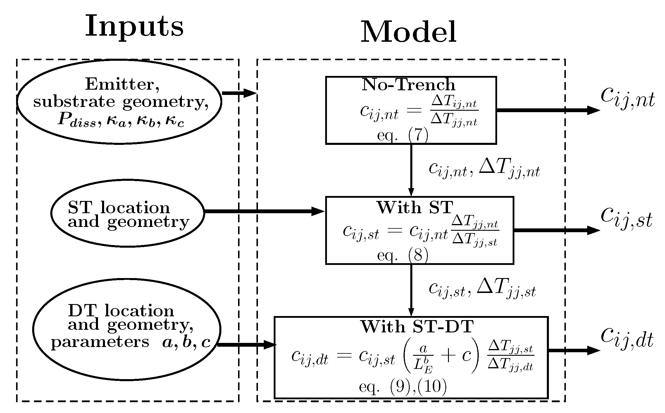
2. Model Formulation

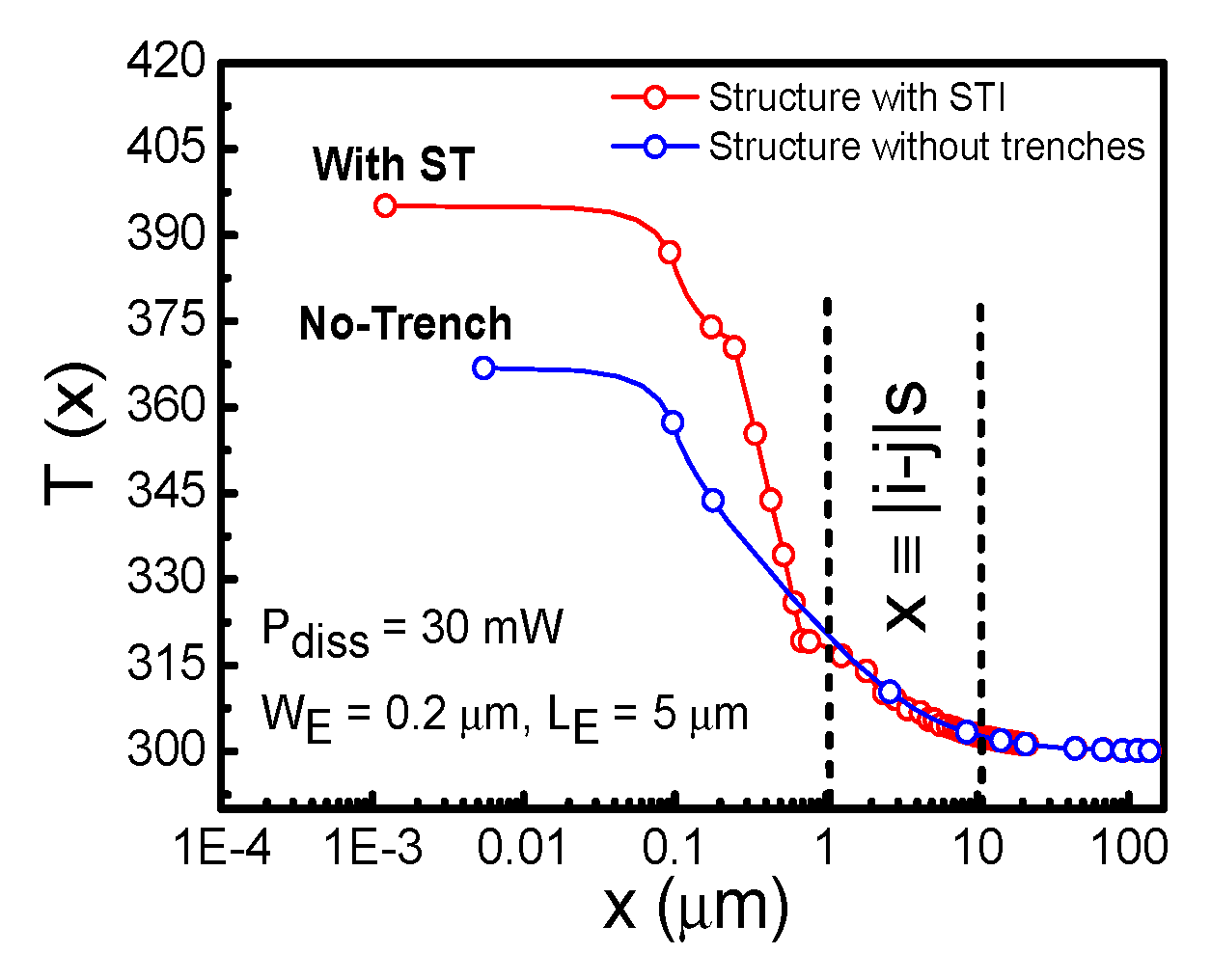
2.1. Vertical Position-Dependent Temperature

Figure 1 shows the cross-section of a heat flow volume, defined by thermal spread with a spreading angle of θ , in a multifinger transistor system when only one finger is heating. We have considered an identical spreading angle along both emitter (heat source) width ( W E ) and length ( L E ) directions. Note that in this formulation, a planar heat source is assumed to be located at z = 0 in order to consider the downward heat flow towards the substrate. In this situation, the temperature profile of the only heating finger along the z-direction is given as
T ( z ) = T r e f + P d i s s R T H ( z )
where T r e f is the known reference temperature at one end of the structure away from the heat source. Note that T r e f = T a m b at z = H .
R T H ( z ) is the position dependent thermal resistance of the device which is given as R T H ( z ) = 1 κ ( T ) a v g f G ( z ) where the so-called geometry factor f G ( z ) is expressed as [22]
f G ( z ) = ln L E W E + 2 z tan ( θ ) W E L E + 2 z tan ( θ ) 2 L E W E tan ( θ )
and 1 κ ( T ) a v g signifies average thermal resistivity as done in [12] and is obtained from the temperature dependent thermal conductivity relation of Si as κ ( T ) = ( κ a + κ b T + κ c T 2 ) 1 [8]. Note that the validity of this κ ( T ) relation with κ a = 0.03 × 10 2 mK/W, κ b = 1.56 × 10 5 m/W and κ c = 1.65 × 10 8 m/KW for intrinsic Si, is well studied in the literature as reported in [9,10]. Substituting the expression of R T H ( z ) obtained with [ 1 / κ ( T ) ] a v g = κ a + ( κ b / 2 ) ( T ( z ) + T r e f ) + ( κ c / 3 ) ( T ( z ) 2 + T ( z ) T r e f + T r e f 2 ) in (3) yields a quadratic expression on T ( z ) as
p T ( z ) 2 + q T ( z ) + r = 0
for which the valid solution reads
T ( z ) = ( q ) q 2 4 p r 2 p
with p = P d i s s f G ( z ) κ c 3 , q = P d i s s f G ( z ) κ b 2 + κ c 3 T r e f 1 and r = P d i s s f G ( z ) κ a + κ b 2 T r e f + κ c 3 T r e f 2 + T r e f . Following the findings of [23] that the thermal resistivity 1 / κ ( T ) of Si linearly varies with T, a similar but pragmatic model for self-heating resistance is derived in [12] by putting κ c = 0 . The model accuracy and associated parameter extraction are also reported in [12]. Here we have additionally included the effect of slight non-linearity of 1 / κ ( T ) with a non-zero κ c only to improve the model accuracy. However, this poses a challenge in parameter extraction for which an alternate κ ( T ) (= β / T α ) model is used and κ a , κ b , κ c parameters are found by optimization from extracted α , β values. Note that the efficacy of this alternate model is established in [23]. To be precise, we have not considered the effects of doping on to these parameters and spreading angle θ in our overall investigation.

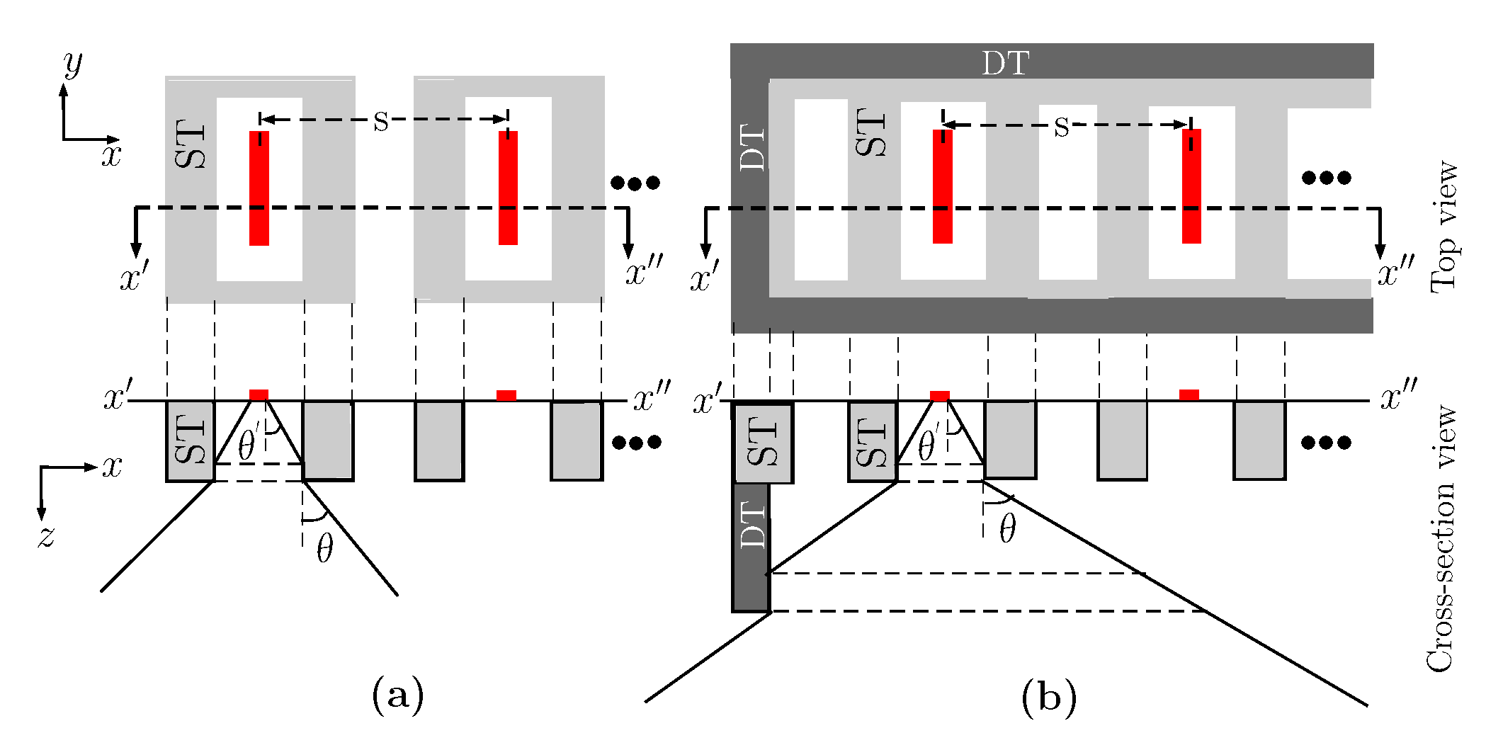
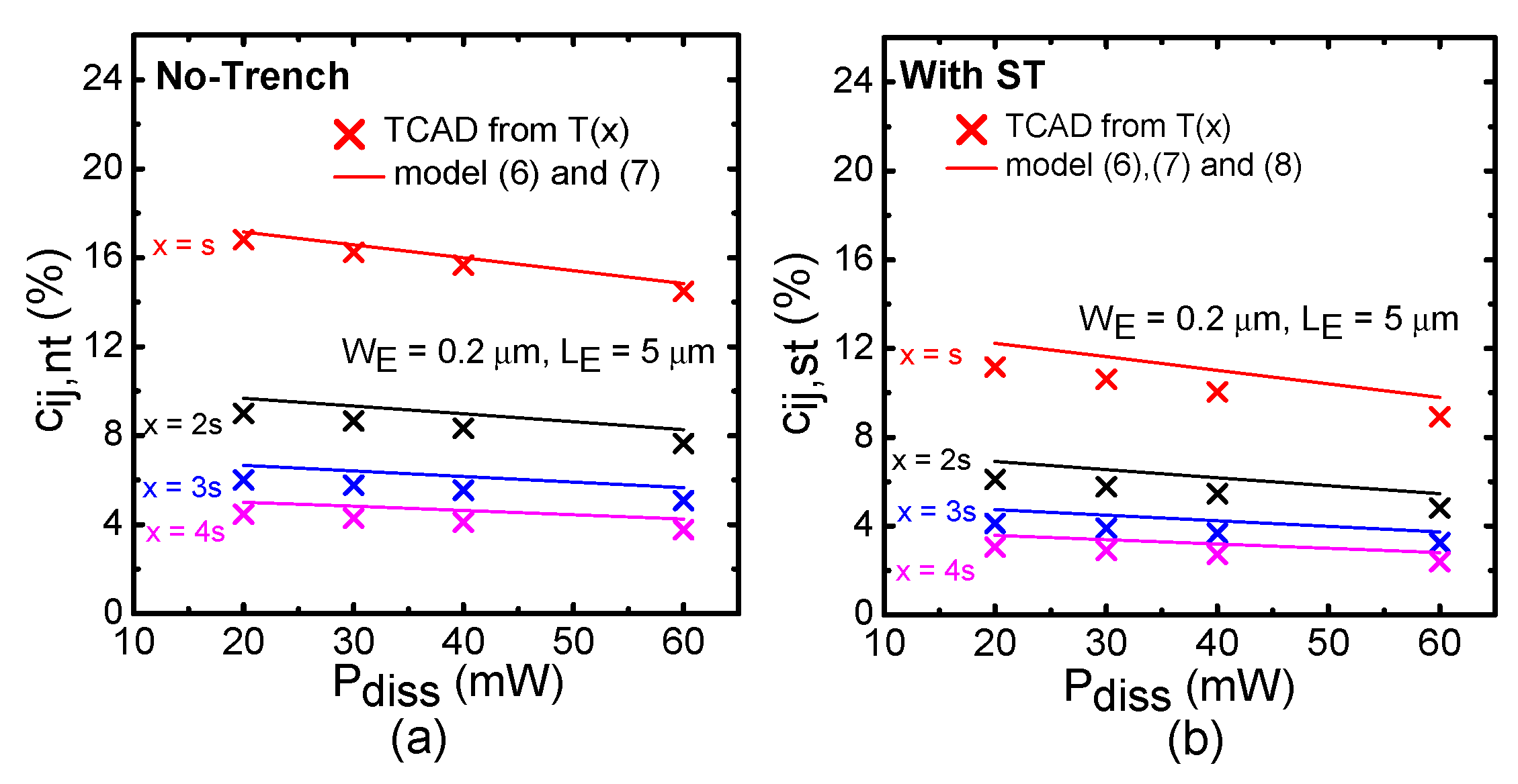
2.2. Coupling Factor for Structures with No-Trench Isolation

For a structure employing no-trench isolation, one can use (6) to obtain the depth-dependent temperature profile T n t ( z ) from the heat source to the heat sink. The rise in junction temperature for the jth heating finger can be obtained as Δ T j j , n t = T n t ( z = 0 ) T a m b . This temperature rise at the heating finger affects the operating temperature of the neighboring fingers through thermal coupling. Following [19], we assume circular isotherms for this structure having no-trench isolation as depicted in Figure 1 resulting into identical temperature profile in the vertical (z-) and lateral (x-) directions, i.e., T n t ( z ) = T n t ( x ) . Therefore, temperature rise at the sensing finger-i due to the heat source at finger-j can be estimated directly from the z-dependent temperature profile of finger-j in (6) as Δ T i j , n t = T n t ( x = z = | i j | s ) T a m b where s is the spacing between the adjacent fingers. Since the maximum distance from the sensing finger to the heat source is just 10 μ m, the assumption of a circular isotherm is justified for all sensing fingers [19]. Finally, the thermal coupling factor between finger-i and finger-j for the multifinger structure with no-trench ( c i j , n t ) can be obtained using (2) as
c i j , n t = Δ T i j , n t Δ T j j , n t T n t ( z = | i j | s ) T a m b T n t ( z = 0 ) T a m b

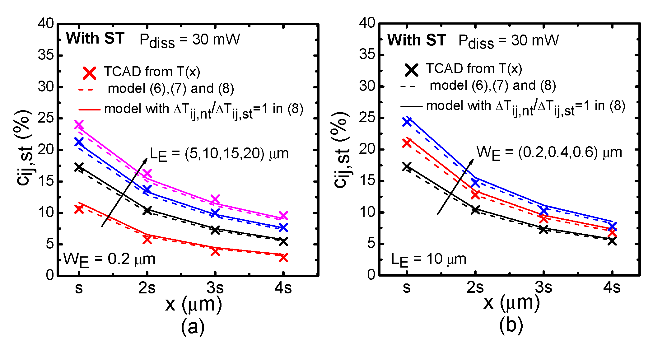
2.3. Coupling Factor for Structures with Shallow Trench Isolation

In the presence of shallow trench (ST) around each finger in a multifinger transistor structure (see Figure 3a), peak junction temperature at the heating finger ( T j j , s t ) happens to be more than that for the structure with no-trench ( T j j , n t ) when excited with the same amount of P d i s s . This results in a temperature profile along the lateral (x-) direction that is different from that in the vertical (z-) direction, i.e., T s t ( x ) T s t ( z ) . The two five-finger devices (one with no-trench and other with ST of 0.36 μ m depth around each finger) with emitter finger dimension as W E × L E = 0.2 × 5 μ m 2 are simulated using TCAD considering T-dependent κ for Si in order to obtain the lateral temperature profiles, T ( x ) , when the corner finger acts as the heat source. Note that T ( x 0 ) T j j (self-heating temperature at the heating finger) and T ( x = | i j | s ) T i j (thermal coupling temperature at the sensing finger). Figure 4 compares the TCAD simulated T ( x ) of the five-finger transistors with no-trench ( T n t ( x ) ) and that with ST ( T s t ( x ) ). It is observed that although T j j , n t < T j j , s t , T i j , n t T i j , s t since T ( x ) values from both structures are almost similar within 1 μ m x 10 μ m. Essentially within the region where neighbouring fingers are located, lateral temperature profiles of both the structures are almost identical, i.e., T n t ( x ) T s t ( x ) for x = s , 2 s , 3 s , 4 s with s = 2.5 μ m (region marked between the two vertical dotted lines in Figure 4). Figure 5a,b demonstrate the ratio Δ T i j , n t / Δ T i j , s t within the range where x = s , 2 s , 3 s , 4 s for various five-finger devices differing in emitter finger dimensions. It is observed that the ratio Δ T n t ( x ) / Δ T s t ( x ) = Δ T i j , n t / Δ T i j , s t 1 . Therefore, following (2) one can obtain the ratio of c i j for the device with no-trench and that with ST as
c i j , n t c i j , s t = Δ T i j , n t Δ T i j , s t Δ T j j , s t Δ T j j , n t Δ T j j , s t Δ T j j , n t .
Since c i j , n t can be estimated using (7), one can find out c i j , s t from (8) just by additionally calculating the rise in self-heating peak (junction) temperature for the two structures (with no-trench and ST). This additional information, i.e., the peak junction temperatures of the two structures are obtained following (6) with z 0 for the respective structures as detailed in [10,11,13].

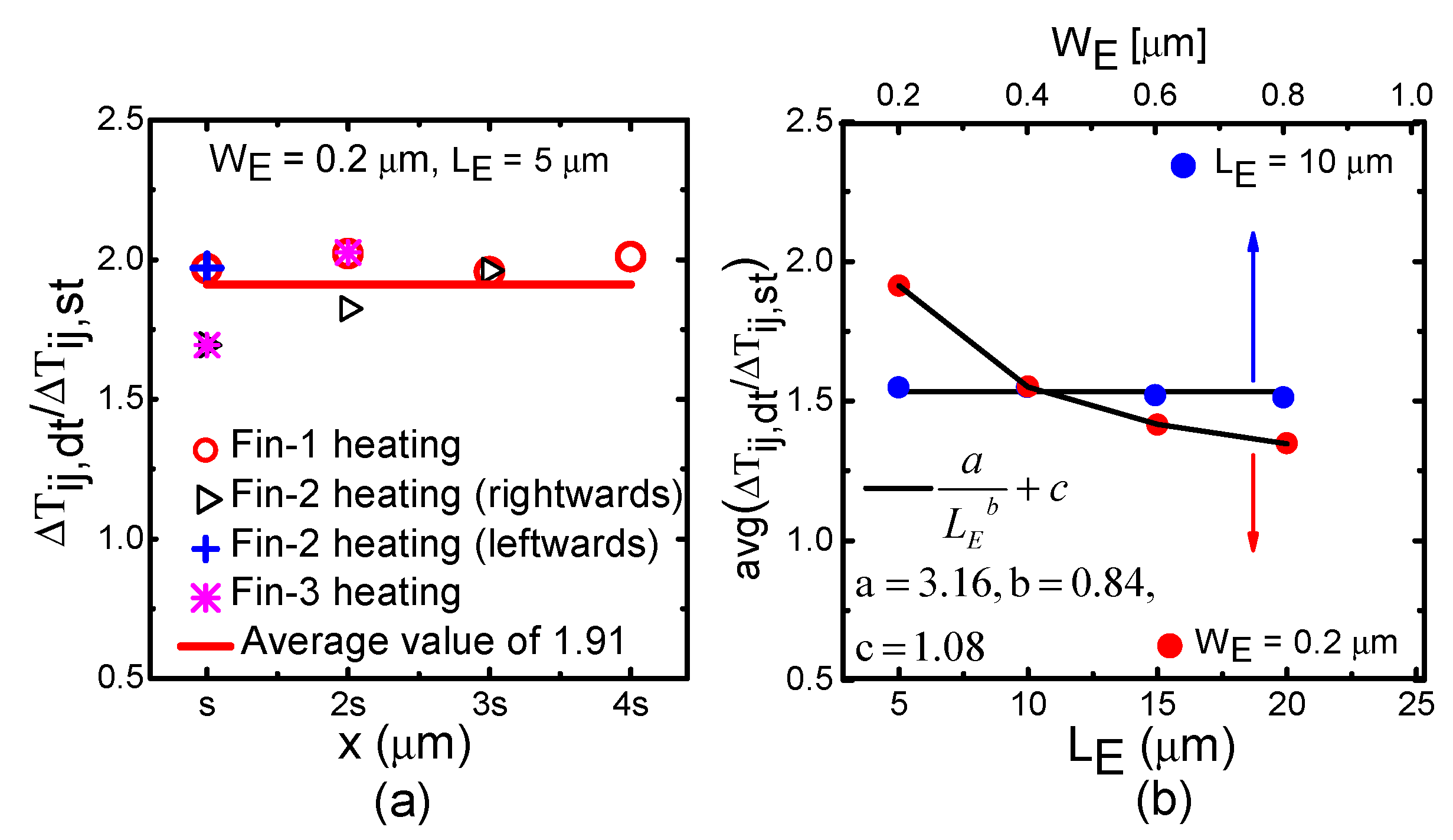
2.4. Coupling Factor for Structures with Additional Deep Trench Isolation

The strategy applied in Section 2.3 for structures containing only ST isolation can be extended to the structures where in addition to the ST surrounding each finger, the complete multifinger transistor is housed within a common deep trench (DT) as seen in Figure 3b. Thermal coupling factor for such a structure is hereafter denoted as c i j , d t . Now defining a ratio between c i j , d t and c i j , s t for two identical multifinger devices except the presence of DT in one structure, we can write
c i j , d t c i j , s t = Δ T i j , d t Δ T i j , s t Δ T j j , s t Δ T j j , d t
where Δ T i j , d t and Δ T j j , d t are temperature rises of sensing and heating fingers, respectively, for the structure housed within additional DT. Note that the first term in the r.h.s. of (9) is not unity unlike that in (8) and is greater than unity due to DT confinement. We simulated the structure containing DT with a height of 3.9 μ m in TCAD and obtained the values of the ratio Δ T i j , d t / Δ T i j , s t as a function of the position of the sensing finger from the heating finger as shown in Figure 6a. In the figure we show the ratio values marked in hollow circles for the case when 1st corner finger is heating and 2nd, 3rd, 4th, 5th are the sensing fingers, respectively, located at distances of s , 2 s , 3 s , 4 s from the heat source. Similarly, points marked in plus (in blue) and triangle symbols are for 2nd heating finger with 1st (towards left), 3rd, 4th, 5th (towards right) as the sensing fingers. Finally, the points marked in asterisk symbol are for 3rd heating finger with 1st and 2nd (towards left) and 4th and 5th (towards right) as the sensing fingers. It is observed that these ratios do not change significantly when different fingers are heating and temperatures at nearby or distant fingers are sensed. The average value of the ratio comes out to be 1.91 . Figure 6b presents the TCAD simulation results for the average value of the ratio Δ T i j , d t / Δ T i j , s t for various emitter (heat source) dimensions ( W E and L E ). Since an increase in the emitter length demands a similar positional shift of the DT walls along the L E direction, overall DTI box volume increases and subsequently the heat confinement is reduced causing the ratio to fall for higher L E devices. However, since W E variation is limited within 1 μ m, the ratio remains almost constant with increasing emitter width. It is also demonstrated in Figure 6b that an empirical model given as
Δ T i j , d t Δ T i j , s t = a L E b + c
accurately captures the L E dependence of this ratio with fitting parameters a, b and c. Therefore, for a given technology the model of the ratio in (10) helps one in modeling c i j , d t with a prior knowledge of c i j , s t and the peak junction temperatures Δ T j j , s t and Δ T j j , d t . Note that Δ T j j , s t and Δ T j j , d t can be obtained by using (6) with appropriate heat spreading angles for the respective structures as detailed in [13]. Although the model parameters, a, b and c in (10) can vary with DT dimensions (height and thickness), usually for a given technology it does not change. The parameters extracted here and depicted in Figure 6b corresponds to DT dimensions of STMicroelectronics B55 technology [24]. From further investigation we found that the unity value of the ratio Δ T i j , n t / Δ T i j , s t is independent of power dissipation. In addition, the ratios avg( Δ T i j , d t / Δ T i j , s t ), c i j , n t / c i j , s t and c i j , d t / c i j , s t do not change with P d i s s . Finally in Figure 7 we present a flowchart for calculating the coupling factors c i j , n t , c i j , s t and c i j , d t following a step-by-step approach using the structural information of the multifinger transistor. The model up to shallow-trench isolated device is physics-based, scalable and requires only the geometry information of the device. For DT-isolated device, the model is partially empirical and additionally requires the technology-specific values of a, b and c parameters which may be obtained using additional effort, e.g., TCAD simulation.

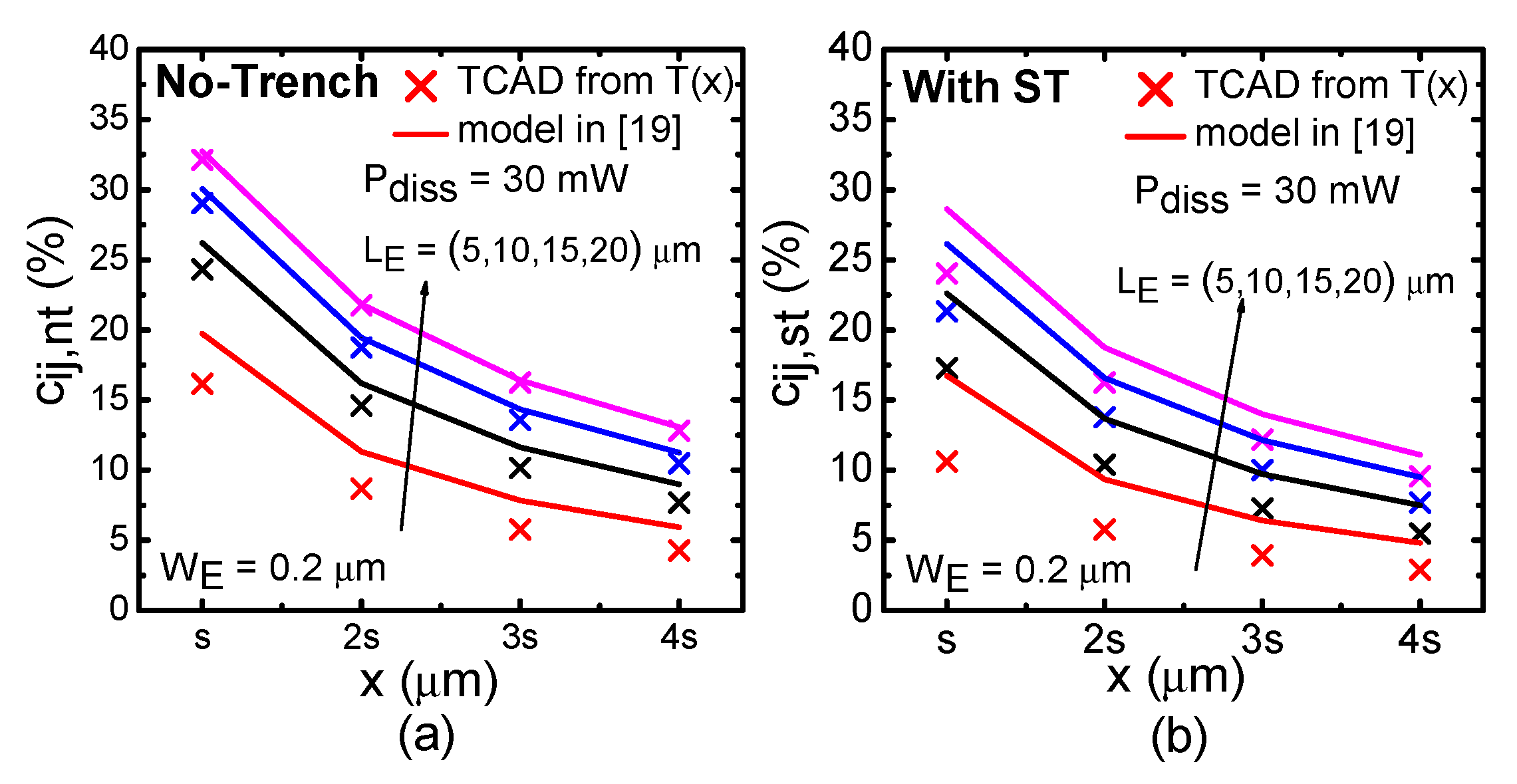
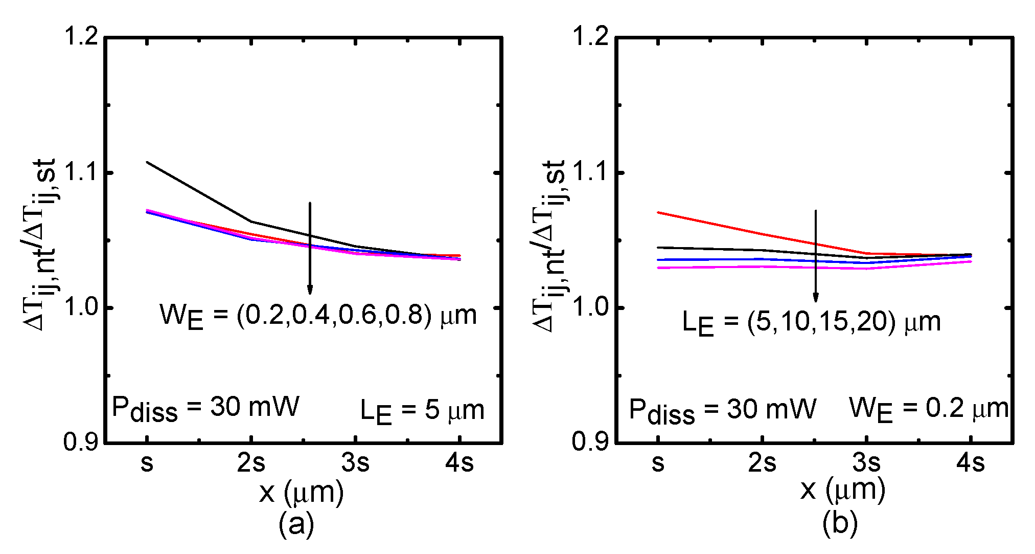
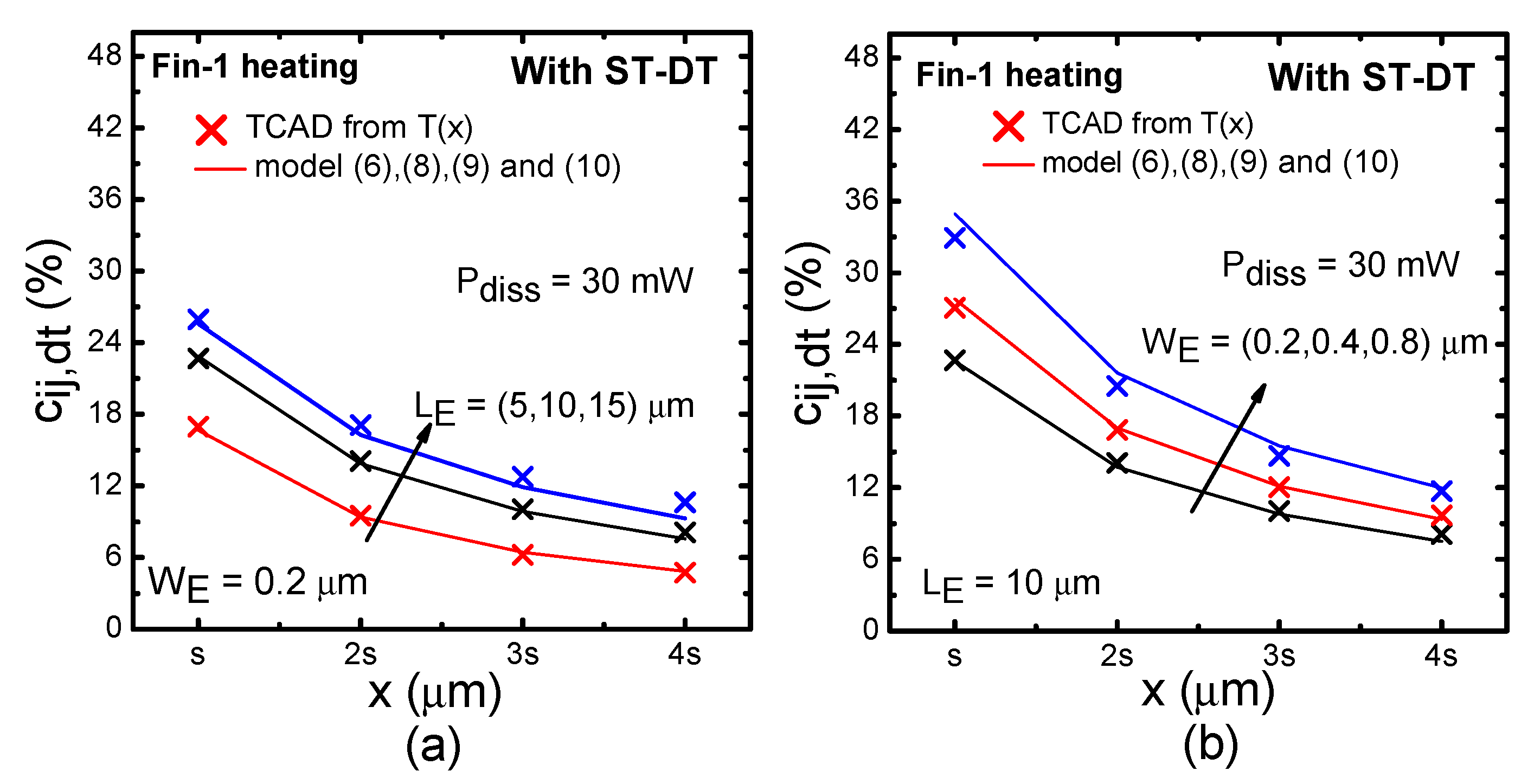
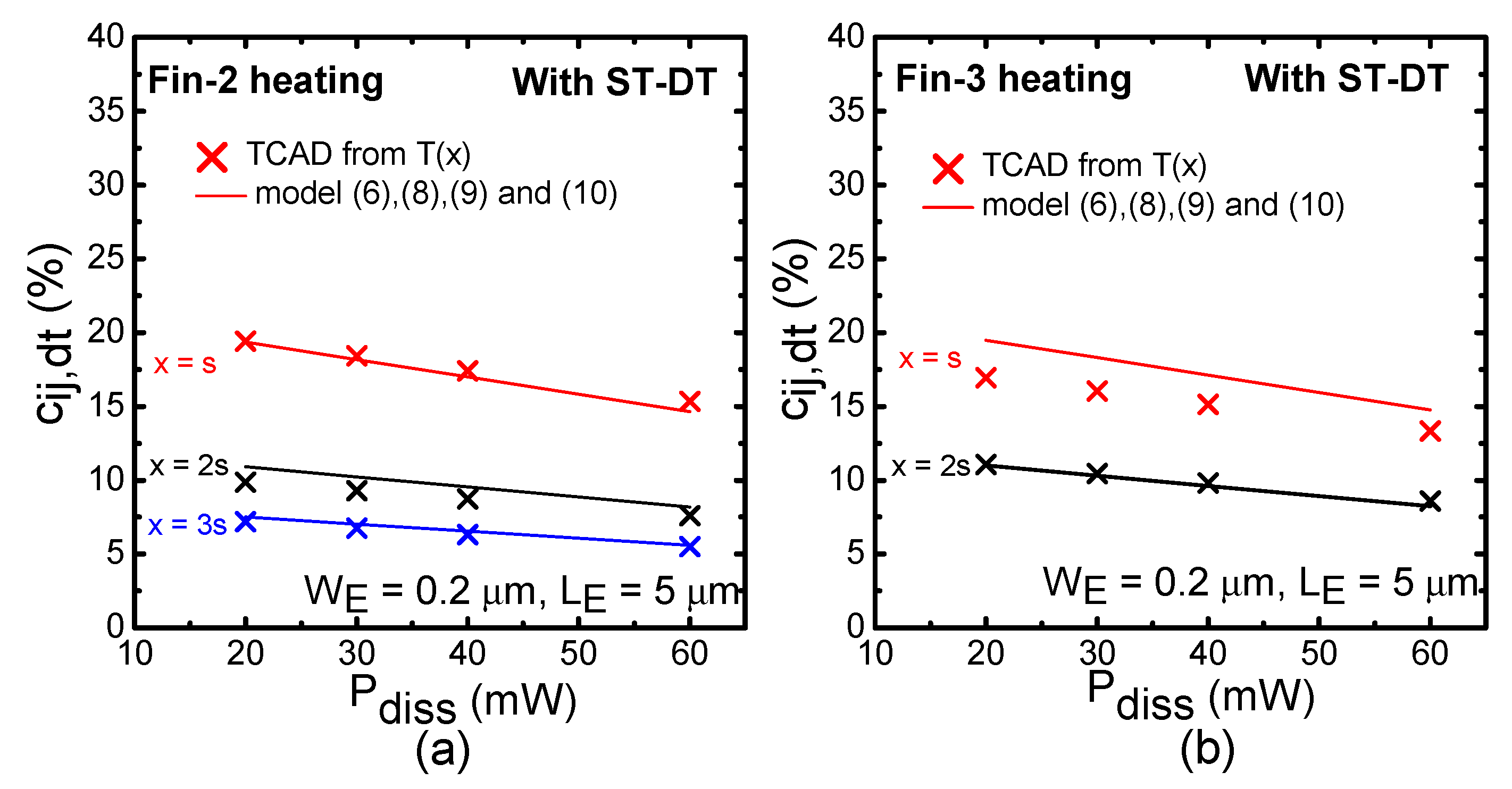
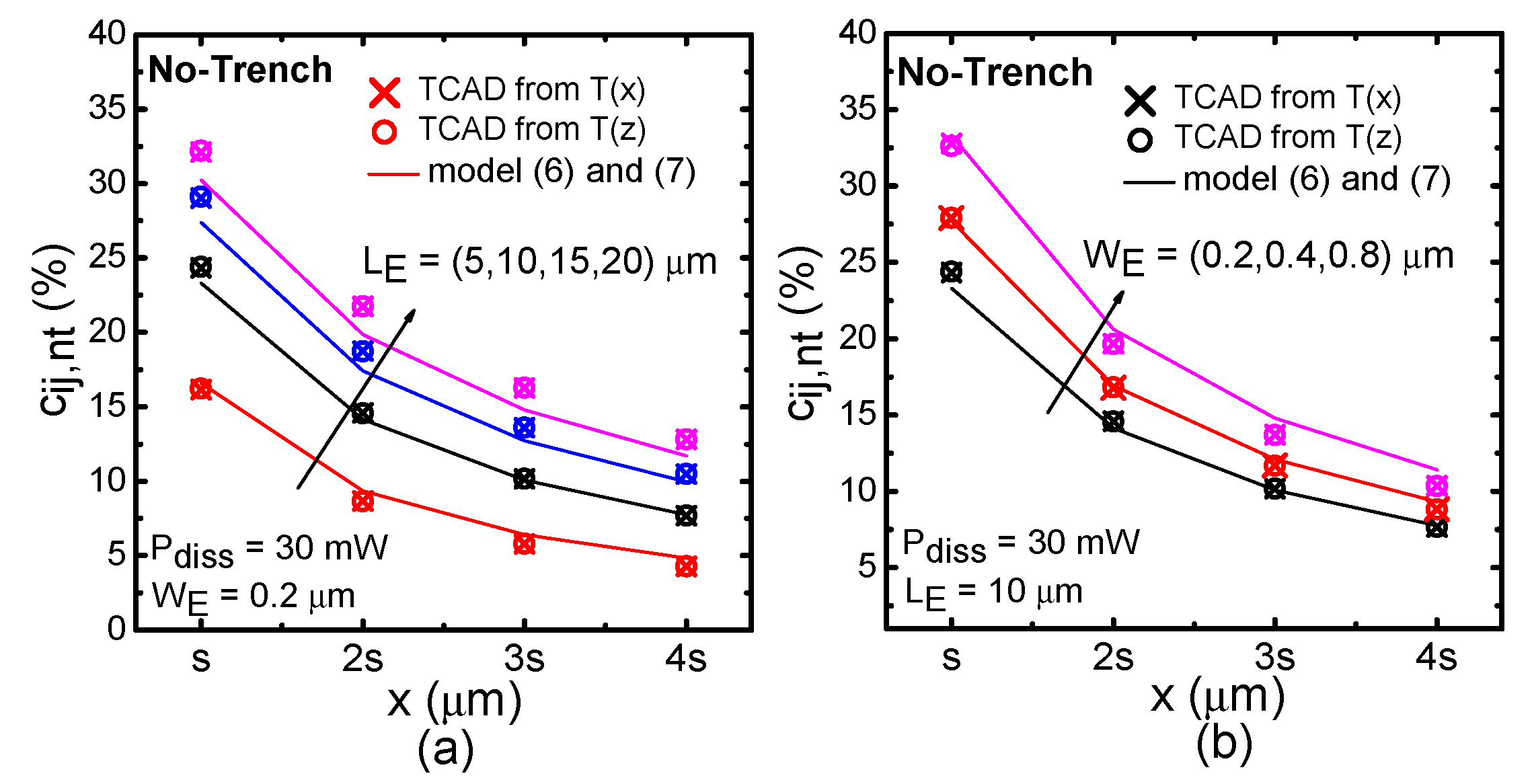
3. Results and Discussion

It is apparent that the accuracy of c i j , n t in (7) depends on the temperature profile T ( z ) under the heating finger which in turn depends largely on the heat spreading angle in (4). One can get an adequate accuracy in the prediction of Δ T j j , n t and c i j , n t by employing a constant heat spreading angle from the heat source to the heat sink. Conventionally although θ = 45 is chosen in several works [9,10,11,19,25], we found that a spreading angle of θ = 48 accurately predicted Δ T j j , n t and c i j , n t for various emitter geometries simulated in TCAD as demonstrated in Figure 8a,b.
In order to calculate the peak junction temperature of the heating finger in case of ST isolated multifinger structure, one can use (6) by sectioning the full vertical region into three parts as carried out in [13]. The value of spreading angle within STI volume was chosen as 35 to consider the evident heat confinement at close proximity to the heat source [26,27,28]. For the substrate region below the ST, spreading angle was kept at 48 following the ones used in the structure with no-trench isolation. Employing (3) for each section resulted in the value of Δ T j j , s t which was used in (8) to estimate c i j , s t . Figure 9 compares the TCAD simulation and the c i j , s t model of (8) using the quantities obtained for the structure with no-trench as detailed in Section 2.2. Results of dashed lines were obtained for accurate values of the ratio Δ T i j , n t / Δ T i j , s t (directly obtained from TCAD) while the solid lines correspond to the approximation, Δ T i j , n t / Δ T i j , s t 1 . Note that the approximation resulted in a decent model agreement with a maximum error of 5 % . Figure 10a,b show the P d i s s -dependent variation of c i j , n t and c i j , s t , respectively. The model (solid line) was found to be in good agreement with the TCAD simulation results (symbols). The reduction of c i j with increasing P d i s s is due to the positional temperature-dependent thermal conductivity of silicon within the device. The same trend has been reported in other works such as [17,18,20].
For the multifinger device housed within DT, we employed the thermal spread model as detailed in Section 2.4 considering adiabatic boundary conditions at DT [13] to estimate Δ T j j , d t . The heat spreading angles within the ST sections were kept at 35 and that for the remaining sections surrounded by DT and below, they were kept at 48 . Thus the values of junction temperatures were obtained for different heating fingers at different power dissipation. Figure 11 compares the TCAD simulation of scaled devices with the modeling results of c i j , d t obtained from (9) and (10) for the case when only the corner (1st) finger acted as the heat source. Figure 12a,b present similar results when the second and third fingers in a five finger structure with DT act as the heat sources, respectively. The model was found to accurately predict the coupling factors in all cases. Note that the modeling results here correspond to the ones obtained after using the approximation Δ T i j , n t / Δ T i j , s t = 1 in (8). The excellent model agreement of all the coupling factors as a function of the spatial dimension as demonstrated in Figure 8, Figure 9 and Figure 11 signifies that even in the case of different spacing between the fingers, the same model can be used to find out the new set of thermal coupling factors. The TCAD validation presented so far illustrates the scalability of the model. The proposed model accurately predicted the coupling coefficients for mainly three types of multifinger structures, without any trenches, with only ST, and with ST and DT. Note that with proper values of the parameters to define the temperature dependent thermal conductivity of a material, the model can be applied to devices based on semiconductors other than Si.

4. Limitations and Future Scope

Since including the temperature-dependence of thermal conductivity of Si ( κ ( T ) ) renders the original heat diffusion equation nonlinear, application of superposition principle to include the effects of self-heating and thermal coupling in calculating the finger temperature in (1) is questionable. Figure 13 compares the TCAD simulation results for P d i s s -dependent third finger temperature when (i) all fingers are heating simultaneously in a ST-isolated five-finger transistor (true temperature) and (ii) one finger is heating at a time and summing up the effects using (1). The maximum error appears to be around 10% for a P d i s s of 30 mW. Note that this error is unavoidable even in the framework of thermal measurement where only one finger is excited with high power and others are used for sensing and where the κ ( T ) effect is automatically included. Although a ratio-based method reported in [20] attempted to additionally include the self-heating effect of the sensing finger, the procedure does not let us get rid of the above-mentioned limitation. It should be noted that the use of 3D Laplace or FEM based iterative solutions can predict accurate finger temperature as TCAD simulation under real operating condition when all fingers are heating simultaneously, however, such techniques cannot be adopted within a compact modeling framework.
Another limitation of the present work lies in the use of the empirical Equation (10) for which the parameters a, b and c corresponding to different technologies are to be extracted possibly using TCAD simulation. In addition, the effect of doping in the T ( z ) model of (1) needs to be investigated.

5. Conclusions

We have developed a scalable model for static thermal coupling factor in trench-isolated multifinger bipolar transistors including the temperature dependence of thermal conductivity of the semiconductor. The overall model is intuitive and simple to implement. At first the model estimates the coupling factor for the transistor structure having no-trench isolation. The model is validated with detailed 3D TCAD simulation. Next the model is extended to predict the thermal coupling effect in multifinger device structures where each finger is surrounded by shallow trench isolation. It is found that a prior knowledge of the coupling coefficient and peak junction temperature for the similar device structure with no-trench and only peak junction temperature for the ST isolated device is sufficient to predict the thermal coupling factor for the ST isolated device. In a similar fashion, we extend the thermal coupling model for deep trench isolated multifinger devices additionally using an empirical scaling rule. Excellent model agreements with TCAD simulation for multifinger devices with different finger dimensions and under different power dissipation demonstrate the utility of the model.

Author Contributions

Conceptualization, A.G., S.B., and A.C.; methodology, S.B., and A.C.; software, A.G., KN., and S.B.; validation, A.G. and KN.; formal analysis, A.G., KN.; investigation, A.G.; resources, S.Y., S.F., and T.Z.; writing—original draft preparation, A.C.; writing—review and editing, S.B., S.F., and T.Z.; visualization, A.G., KN., S.B., and A.C.; supervision, S.B. and A.C.; project administration, A.C.; funding acquisition, A.C., S.F., and T.Z. All authors have read and agreed to the published version of the manuscript.

Funding

This work was supported in part by the EU under Project Taranto under Grant 737454, in part by ISRO project ELE/17-18/176/ISRO/ANJA and in part by DST, India, under Project EMR/2016/004726.

Conflicts of Interest

The authors declare no conflict of interest.

References

  1. Harame, D.L.; Comfort, J.; Cressler, J.; Crabbe, E.; Sun, J.C.; Meyerson, B.; Tice, T. Si/SiGe epitaxial-base transistors. II. Process integration and analog applications. IEEE Trans. Electron Devices 1995, 42, 469–482. [Google Scholar] [CrossRef]
  2. Lachner, R. Towards 0.7 THz Silicon Germanium Heterojunction Bipolar Technology—The DOTSEVEN Project. ECS Trans. 2014, 64, 21–37. [Google Scholar] [CrossRef]
  3. Wilson, L. International Technology Roadmap for Semiconductors (ITRS) 2013. Available online: http://www.itrs2.net/2013-itrs.html (accessed on 14 July 2020).
  4. Chevalier, P.; Meister, T.; Heinemann, B.; Van Huylenbroeck, S.; Liebl, W.; Fox, A.; Sibaja-Hernandez, A.; Chantre, A. Towards THz SiGe HBTs. In Proceedings of the Bipolar/BiCMOS Circuits and Technology Meeting (BCTM), Atlanta, GA, USA, 9–11 October 2011; pp. 57–65. [Google Scholar]
  5. Joy, R.C.; Schlig, E. Thermal properties of very fast transistors. IEEE Trans. Electron Devices 1970, 17, 586–594. [Google Scholar] [CrossRef]
  6. Walkey, D.J.; Celo, D.; Smy, T.J.; Surridge, R.K. A thermal design methodology for multifinger bipolar transistor structures. IEEE Trans. Electron Devices 2002, 49, 1375–1383. [Google Scholar] [CrossRef]
  7. Smy, T.; Walkey, D.; Dew, S.K. A 3D thermal simulation tool for integrated devices–Atar. IEEE Trans. Comput.-Aided Des. Integr. Circuits Syst. 2001, 20, 105–115. [Google Scholar] [CrossRef]
  8. Synopsys. Sentaurus: Sentaurus Device User Guide, Release H-2013.03; Synopsys: Mountain View, CA, USA, 2013. [Google Scholar]
  9. Sahoo, A.K.; Fregonese, S.; Weiss, M.; Maneux, C.; Zimmer, T. A Scalable Model for Temperature Dependent Thermal Resistance of SiGe HBTs. In Proceedings of the Bipolar/BiCMOS Circuits and Technology Meeting (BCTM), Bordeaux, France, 30 September–3 October 2013; pp. 29–32. [Google Scholar] [CrossRef]
  10. Chakravorty, A.; D’Esposito, R.; Balanethiram, S.; Frégonèse, S.; Zimmer, T. Analytic Estimation of Thermal Resistance in HBTs. IEEE Trans. Electron Devices 2016, 63, 2994–2998. [Google Scholar] [CrossRef]
  11. Balanethiram, S.; Chakravorty, A.; D’Esposito, R.; Fregonese, S.; Céli, D.; Zimmer, T. Accurate modeling of thermal resistance for on-wafer SiGe HBTs using average thermal conductivity. IEEE Trans. Electron Devices 2017, 64, 3955–3960. [Google Scholar] [CrossRef] [Green Version]
  12. Yadav, S.; Chakravorty, A. A pragmatic approach to modeling self-heating effects in SiGe HBTs. IEEE Trans. Electron Devices 2017, 64, 4844–4849. [Google Scholar] [CrossRef]
  13. Balanethiram, S.; Chakravorty, A.; D’Esposito, R.; Fregonese, S.; Zimmer, T. An improved scalable self-consistent iterative model for thermal resistance in SiGe HBTs. In Proceedings of the Bipolar/BiCMOS Circuits and Technology Meeting (BCTM), New Brunswick, NJ, USA, 25–27 September 2016; pp. 150–153. [Google Scholar] [CrossRef] [Green Version]
  14. Lehmann, S.; Weiss, M.; Zimmermann, Y.; Pawlak, A.; Aufnger, K.; Schroter, M. Scalable compact modeling for SiGe HBTs suitable for microwave radar applications. In Proceedings of the Topical Meeting on Silicon Monolithic Integrated Circuits in RF Systems, Phoenix, AZ, USA, 17–19 January 2011; pp. 113–116. [Google Scholar] [CrossRef]
  15. Walkey, D.J.; Smy, T.J.; Dickson, R.G.; Brodsky, J.S.; Zweidinger, D.T.; Fox, R.M. Equivalent circuit modeling of static substrate thermal coupling using VCVS representation. IEEE J. Solid State Circuits 2002, 37, 1198–1206. [Google Scholar] [CrossRef]
  16. Zimmermann, Y. Modeling of Spatially Distributed and Sizing Effects in High-Performance Bipolar Transistors. Master’s Thesis, Chair Electron Devices Integrated Circuits, Technische Universität, Dresden, Germany, 2004. [Google Scholar]
  17. Weiss, M.; Sahoo, A.K.; Maneux, C.; Fregonese, S.; Zimmer, T. Mutual thermal coupling in SiGe:C HBTs. In Proceedings of the Symposium on Microelectronics Technology and Devices (SBMicro), Curitiba, Brazil, 2–6 September 2013; pp. 1–4. [Google Scholar] [CrossRef]
  18. Dwivedi, A.; Chakravorty, A.; D’Esposito, R.; Sahoo, A.K.; Fregonese, S.; Zimmer, T. Effects of BEOL on self-heating and thermal coupling in SiGe multi-finger HBTs under real operating condition. Solid State Electron. 2016, 115, 1–6. [Google Scholar] [CrossRef]
  19. Goh, G.; Kim, U.; Jeon, M.S.; Kim, J. A simple extraction method of thermal resistance in multifinger GaAs HBT. IEEE Trans. Electron Devices 2016, 63, 2620–2624. [Google Scholar] [CrossRef]
  20. Lehmann, S.; Zimmermann, Y.; Pawlak, A.; Schroter, M. Characterization of the static thermal coupling between emitter fingers of bipolar transistors. IEEE Trans. Electron Devices 2014, 61, 3676–3683. [Google Scholar] [CrossRef]
  21. Gupta, A.; Nidhin, K.; Balanethiram, S.; Yadav, S.; Chakravorty, A.; Fregonese, S.; Zimmer, T. Static Thermal Coupling Factors in Multi-FingerBipolar Transistors: Part II—Experimental Validation. J. Electron. 2020. submitted. [Google Scholar]
  22. Gao, G.B.; Ünlü, M.S.; Morkoc, H.; Blackburn, D.L. Emitter ballasting resistor design for, and current handling capability of AlGaAs/GaAs power heterojunction bipolar transistors. IEEE Trans. Electron Devices 1991, 38, 185–196. [Google Scholar] [CrossRef]
  23. Walkey, D.J.; Smy, T.J.; Macelwee, T.; Maliepaard, M. Compact representation of temperature and power dependence of thermal resistance in Si, Inp and GaAs substrate devices using linear models. Solid State Electron. 2002, 46, 819–826. [Google Scholar] [CrossRef]
  24. Chevalier, P.; Avenier, G.; Ribes, G.; Montagné, A.; Canderle, E.; Céli, D.; Derrier, N.; Deglise, C.; Durand, C.; Quémerais, T.; et al. A 55 nm triple gate oxide 9 metal layers SiGe BiCMOS technology featuring 320 GHz fT/370 GHz fmax HBT and high-Q millimeter-wave passives. In Proceedings of the 2014 IEEE International Electron Devices Meeting IEDM, San Francisco, CA, USA, 15–17 December 2014; pp. 3.9.1–3.9.3. [Google Scholar]
  25. Rieh, J.S.; Johnson, J.; Furkay, S.; Greenberg, D.; Freeman, G.; Subbanna, S. Structural dependence of the thermal resistance of trench-isolated bipolar transistors. In Proceedings of the Bipolar/BiCMOS Circuits and Technology Meeting (BCTM), Minneapolis, MN, USA, 1 October 2002; pp. 100–103. [Google Scholar] [CrossRef]
  26. Sahoo, A.K.; Fregonese, S.; Weis, M.; Malbert, N.; Zimmer, T. A Scalable Electrothermal Model for Transient Self-Heating Effects in Trench-Isolated SiGe HBTs. IEEE Trans. Electron Devices 2012, 59, 2619–2625. [Google Scholar] [CrossRef] [Green Version]
  27. Couret, M.; Fischer, G.; Frégonése, S.; Zimmer, T.; Maneux, C. Physical, small-signal and pulsed thermal impedance characterization of multi-finger SiGe HBTs close to the SOA edges. In Proceedings of the 2019 IEEE 32nd International Conference on Microelectronic Test Structures (ICMTS), Kita-Kyushu City, Fukuoka, Japan, 18–21 March 2019; pp. 154–159. [Google Scholar] [CrossRef] [Green Version]
  28. Mukherjee, C.; Couret, M.; Nodjiadjim, V.; Riet, M.; Dupuy, J.Y.; Fregonese, S.; Zimmer, T.; Maneux, C. Scalable Modeling of Thermal Impedance in InP DHBTs Targeting Terahertz Applications. IEEE Trans. Electron Devices 2019, 66, 2125–2131. [Google Scholar] [CrossRef] [Green Version]
Figure 1. Schematic cross-section of a multifinger transistor structure with finger spacing s and having no-trench isolation. Heat source is located at z = 0 . In addition, the isotherms linking the heating finger and the sensing fingers are systematically shown.
Electronics 09 01333 g001
Figure 2. Results of the heat-source geometry dependent c i j model in [19] (lines) compared with corresponding 3D TCAD simulation results (symbols) at different sensing fingers in five-finger transistor structures (a) without any trench isolation and (b) with only shallow trench isolated (STI). Finger spacing s = 2.5 μ m.
Electronics 09 01333 g002
Figure 3. Top view (xy plane) and cross-sectional view (xz plane) of multifinger structure containing (a) only shallow trench and (b) both shallow and deep trenches. Emitter fingers are marked in red. Different sections of the thermal spread with their corresponding spreading angles are also illustrated.
Electronics 09 01333 g003
Figure 4. Temperature profile along x-direction obtained from 3D TCAD simulations of transistors without trenches and with STI.
Electronics 09 01333 g004
Figure 5. The rise in temperature ratio at the sensing fingers of transistors with no-trench and with ST ( Δ T i j , n t / Δ T i j , s t ) obtained from TCAD for (a) different W E at a fixed L E = 5 μ m and (b) different L E at a fixed W E = 0.2 μ m. Finger spacing s = 2.5 μ m.
Electronics 09 01333 g005
Figure 6. (a) Δ T i j , d t / Δ T i j , s t obtained from TCAD (symbols) when finger-1, 2, 3 are heating (one at a time). Overall average of this ratio combining all the three cases is represented by the solid line. Finger spacing s = 2.5 μ m. (b) Overall average of Δ T i j , d t / Δ T i j , s t ratio for transistors with different W E and L E .
Electronics 09 01333 g006
Figure 7. Step-by-step illustration to calculate thermal coupling factor in multifinger transistor structure with no-trench, with shallow trench (ST) and with ST and deep trench (DT). Note that the rise in junction temperature due to self-heating Δ T j j in any structure can be obtained using (6) with z 0 .
Electronics 09 01333 g007
Figure 8. Comparison of c i j , n t obtained from TCAD (symbols) and the proposed model in (6) and (7) (lines) for transistors with (a) different L E at a fixed W E = 0.2 μ m, (b) different W E at a fixed L E = 10 μ m. Finger spacing s = 2.5 μ m.
Electronics 09 01333 g008
Figure 9. Comparison of c i j , s t obtained from TCAD (symbols) and the proposed model in (6)–(8) (lines) for transistors with (a) different L E at a fixed W E = 0.2 μ m and (b) different W E at a fixed L E = 10 μ m. Solid lines correspond to the case when Δ T i j , n t / Δ T i j , s t = 1 in (8). Finger spacing s = 2.5 μ m.
Electronics 09 01333 g009
Figure 10. Dissipated power dependent (a) c i j , n t and (b) c i j , s t at different sensing fingers. A comparison between TCAD simulation results (symbols) and the proposed model (solid lines). Solid lines in (b) correspond to the case when Δ T i j , n t / Δ T i j , s t = 1 in (8).
Electronics 09 01333 g010
Figure 11. Comparison of c i j , d t obtained from TCAD (symbols) and the proposed model in (6)–(10) (lines) when finger-1 is heating in five-finger transistors with (a) different L E at a fixed W E = 0.2 μ m, (b) different W E at a fixed L E = 10 μ m. Solid lines correspond to the case when Δ T i j , n t / Δ T i j , s t = 1 in (8). Finger spacing s = 2.5 μ m.
Electronics 09 01333 g011
Figure 12. P d i s s -dependent c i j , d t for a five-finger device structure when (a) second finger acts as the heat source and (b) third finger acts as the heat source: comparison between TCAD (symbols) and model of (6)–(10) using a constant value for Δ T i j , d t / Δ T i j , s t in (9). Solid lines correspond to the case when Δ T i j , n t / Δ T i j , s t = 1 in (8).
Electronics 09 01333 g012
Figure 13. P d i s s —dependent total junction temperature T i , s t of the third finger in a five-finger structure with ST isolation. Symbols are TCAD values when all fingers are heating and the solid line is obtained from (1) by substituting TCAD values of Δ T i i and Δ T i j .
Electronics 09 01333 g013

