Partial Isolation Type Saddle-FinFET(Pi-FinFET) for Sub-30 nm DRAM Cell Transistors
by
Young Kwon Kim
1, 
Jin Sung Lee
1,
Geon Kim
1,
Taesik Park
2,*,
Hui Jung Kim
3,
Young Pyo Cho
4,
Young June Park
3 and
Myoung Jin Lee
1,* 1
School of Electronics and Computer Engineering, Chonnam National University, Gwangju 500-757, Korea
2
Department of Electrical and Control Engineering, Mokpo National University, Jeollanam-do 534-729, Korea
3
School of Electrical Engineering, Seoul National University, Seoul 151-742, Korea
4
The KEPCO Research Institute, Daejeon 305-760, Korea
*
Authors to whom correspondence should be addressed.
Electronics 2019, 8(1), 8; https://doi.org/10.3390/electronics8010008
Submission received: 1 November 2018
/
Revised: 13 December 2018
/
Accepted: 19 December 2018
/
Published: 21 December 2018
(This article belongs to the Special Issue Nanoelectronic Materials, Devices and Modeling)
Abstract
:In this paper, we proposed a novel saddle type FinFET (S-FinFET) to effectively solve problems occurring under the capacitor node of a dynamic random-access memory (DRAM) cell and showed how its structure was superior to conventional S-FinFETs in terms of short channel effect (SCE), subthreshold slope (SS), and gate-induced drain leakage (GIDL). The proposed FinFET exhibited four times lower Ioff than modified S-FinFET, called RFinFET, with more improved drain-induced barrier lowering (DIBL) characteristics, while minimizing Ion reduction compared to RFinFET. Our results also confirmed that the proposed device showed improved drain-induced barrier lowering (DIBL) and Ioff characteristics as gate channel length decreased.
Keywords:
gate-induced drain leakage (GIDL); drain-induced barrier lowering (DIBL); recessed channel array transistor (RCAT); on-current (Ion); off-current (Ioff); subthreshold slope (SS); threshold voltage (VTH); saddle FinFET (S-FinFET); potential drop width (PDW); shallow trench isolation (STI); source/drain (S/D)1. Introduction
With decreasing dynamic random-access memory (DRAM) cell size, a recessed channel array transistor (RCAT) has been proposed to overcome the short channel effect (SCE) of conventional MOSFETs with planar channels. Although the recessed channel of RCAT has improved short channel effect (SCE), RCAT suffers from low driving current and VTH sensitivity due to the shape of the bottom corner of the recessed channel [1]. To solve these problems, a saddle FinFET (S-FinFET) has been proposed with a tri-gate that wraps both the recessed channel surface and the side surface [2,3,4]. S-FinFET not only exhibits excellent short channel effect characteristics, but also maintains excellent subthreshold swing (SS), high Ion, and nearly constant VTH. However, S-FinFET has higher gate-induced drain leakage (GIDL) than RCAT because the overlap region between the gate and drain regions is wider in S-FinFET. Although modified S-FinFET, called RFinFET, has emerged to reduce leakage by GIDL, RFinFET still needs to operate in sub-30 nm cell size [5,6]. Minimizing Ioff in DRAM applications is a critical issue to achieving long refresh time. If this problem is not addressed, conventional S-FinFETs, including S-FinFET and RFinFET, will experience significant drawbacks in the application of DRAM technology. Therefore, a new device structure with an improved Ioff is required. In this paper, we proposed a new device with a partial isolation region under the storage node of conventional S-FinFET. This structure can be fabricated by using an isotropic dry etching technique for the buried insulator under the cell transistor [7,8]. We analyzed electrical characteristics of this proposed device and compared them with those of conventional S-FinFETs of the same size. We also showed the optimized parameters of the buried insulator using a three-dimensional (3D) device simulator in sub-30 nm cell size [9]. The device described in this paper has reliable source/drain (S/D) doping concentration with a Gaussian profile. The simulator is well tuned to predict DRAM cell transistor leakage distribution [10,11].
2. Device Structure
The partial isolation type S-FinFET (Pi-FinFET) is a structure with a buried insulator at a certain depth from the storage node of a conventional S-FinFET. Figure 1a shows a 3D schematic of a Pi-FinFET. Silicon film thickness, buried insulator thickness, and Lin, as shown in Figure 1a,b, are defined as the distance from the contact surface of the storage node to the buried insulator, the thickness of the buried insulator in the direction perpendicular to the channel, and the distance from the side gate oxide to the buried insulator, respectively. Lg, Lside, Lov_xj, and Lov_side represent gate channel length, the length of the side-gate in the direction parallel to the channel, the overlapped length of the side-gate and S/D doping region shown in Figure 1a, and the side-channel width shown in Figure 1c, respectively. When Lside and Lov_xj are increased, the width of the overlap region of the gate and the S/D region will also increase. The n+ poly gate with a gate work function of 4.2 eV was applied. Lg, Lside, Lov_side and the recessed depth are 30 nm, 42 nm, 10 nm, and 100 nm, respectively. RFinFET is the modified S-FinFET with a structure in which the overlap region between the side-gate and the S/D region is removed [5]. Therefore, the Pi-FinFETs proposed in this paper can be divided into Pi-SFinFET and Pi-RFinFET depending on the presence or absence of the overlap region between the side-gate and the S/D region. Namely, in this paper, the Lov_xj of Pi-RFinFET is 0 nm and that of Pi-SFinFET is 70 nm.
3. Results and Discussion
Log and linear ID-VGS curves shown in Figure 2 are the result of comparing conventional S-FinFETs and RCAT with the Pi-FinFETs proposed in this paper. Silicon film thickness, buried insulator thickness, and Lin of Pi-FinFET was set at 20 nm, 100 nm, and 20 nm, respectively. As shown in Figure 2, the four saddle type FinFETs have significantly higher Ion than RCAT. Moreover, the dotted red ellipse in Figure 2 show that Pi-SFinFET has about three times smaller Ioff than S-FinFET, while Pi-RFinFET has about four times smaller Ioff than RFinFET at VGS of −0.5 V. To understand physical characteristics of Ioff reduction for Pi-FinFET, device simulations have been performed using the TCAD tool [9,10]. The 3-D simulator is well tuned to predict the leakage current such as GIDL by applying the Hurkx band-to-band tunneling model.
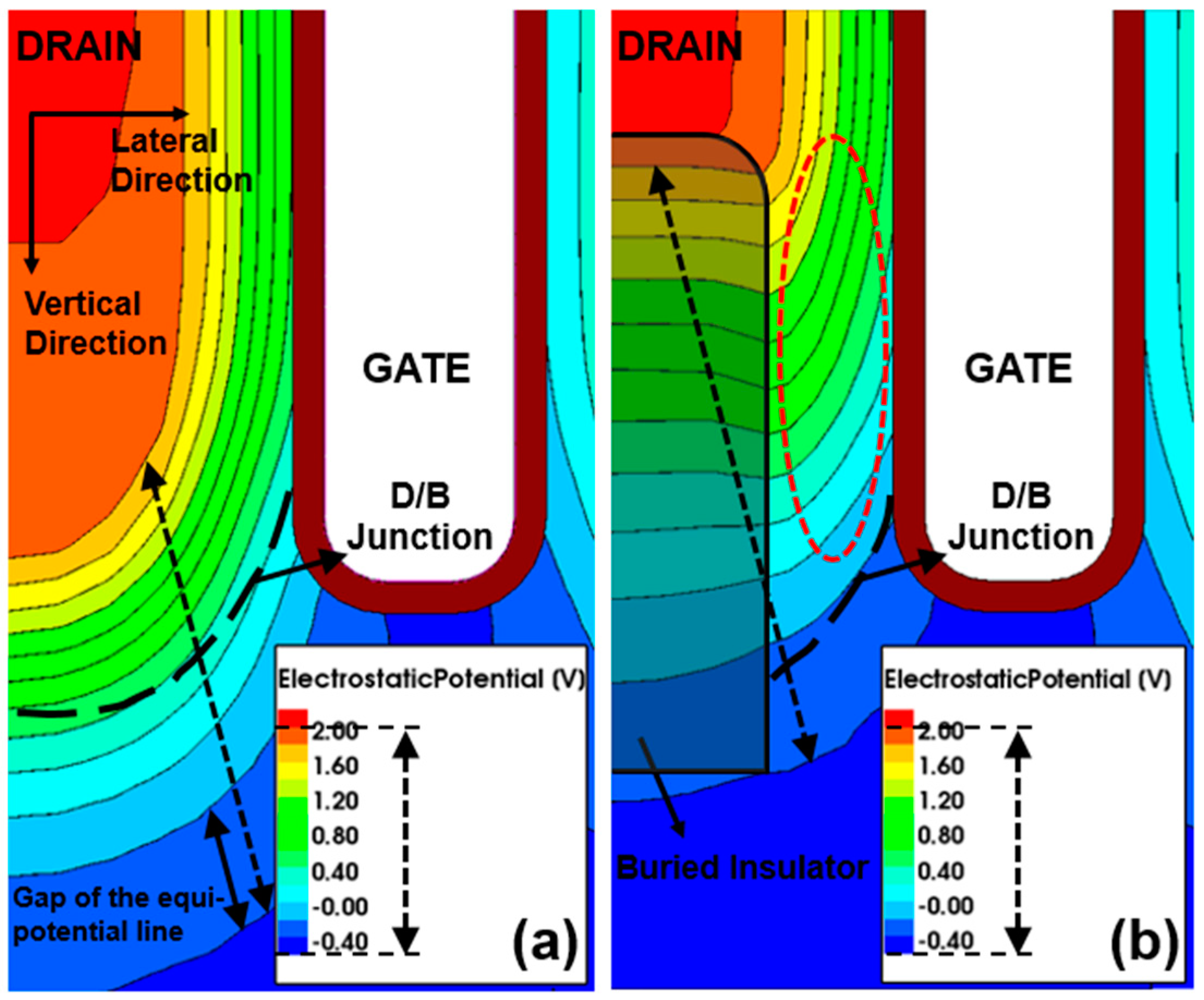
Figure 3 shows the simulated potential contour near the drain region of conventional S-FinFET and Pi-FinFET at VDS of 1.5 V and VGS of −0.5 V. We defined the gap of equipotential lines as the potential drop width (PDW). In particular, dotted arrows in Figure 3a,b indicate PDW from 1.8 V to −0.4 V. As shown in Figure 3a, the conventional S-FinFET has intensive and narrow PDW from 1.8 V to −0.4 V near the drain/body (D/B) junction. On the other hand, PDW is mostly limited by the buried insulator of Pi-FinFET, as shown in Figure 3b. Namely, the rather constant electric field in the buried insulator of Pi-FinFET induces a wider PDW near the drain region [12]. The dotted red ellipse in Figure 3b shows that the PDW is wider in the silicon layer compared to the conventional S-FinFET. In other words, Pi-FinFET can reduce the electric field affecting GIDL in the silicon layer between the gate and drain regions. Moreover, the penetration of the electric field from the drain to the source affecting drain-induced barrier lowering (DIBL) is minimized in Pi-FinFET.
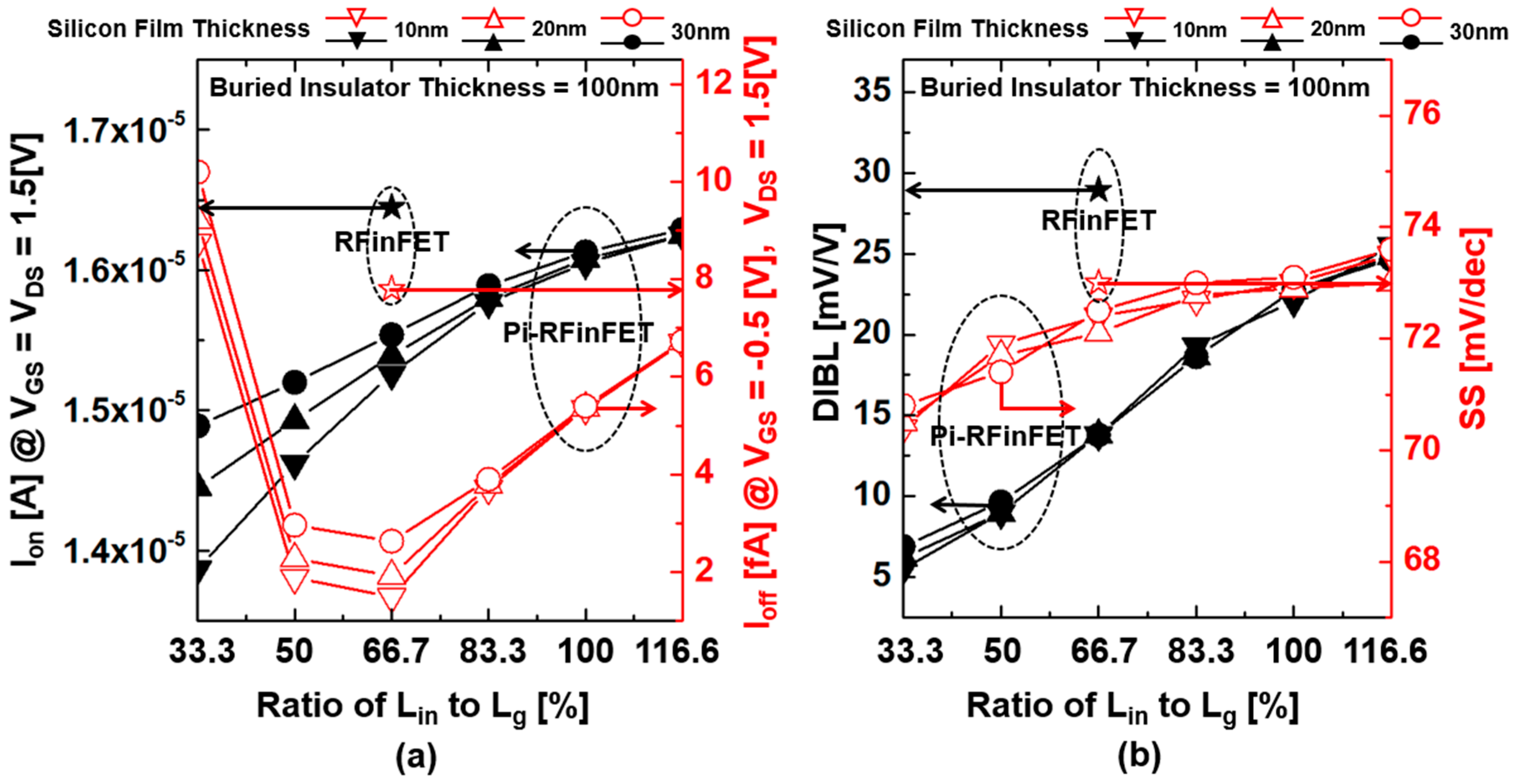
Figure 4a shows that Ioff and Ion decrease as Lin decreases when Lg is 30 nm. If the ratio of Lin to Lg is as small as 50% or less, the lateral PDW of the silicon layer induced by the buried insulator will become narrow. This is because the deep penetration of the buried insulator limits the lateral PDW in the narrow silicon layer between the gate and drain regions. As a result, it induces abnormal Ioff increase and Ion decrease, as shown in Figure 4a. Therefore, in order to maintain a relatively high Ion while maintaining a low Ioff, it is desirable to define the ratio of Lin to Lg to 50 to 83.3%, respectively. As shown in Figure 4a, Ioff is minimized when the ratio of Lin to Lg is 66.7%. As shown in Figure 4b, DIBL and SS characteristics are consistently improved because of wider PDW when Lin is decreased. Figure 5 shows Ioff and DIBL characteristics according to Lg at VDS of 1.5 V and VGS of −0.5 V. Lin values in Figure 5 were set to maintain 60% of Lg. Pi-FinFETs consistently exhibited improved Ioff and DIBL characteristics compared to conventional S-FinFETs regardless of Lg. Especially, Pi-FinFETs exhibited improved DIBL characteristics with opposite tendency compared to conventional S-FinFETs as Lg decreases, as shown in Figure 5b.
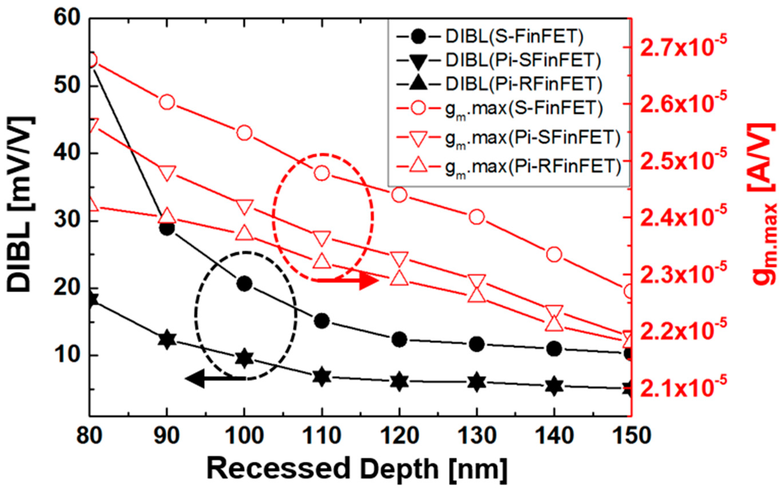
Figure 6 also shows the DIBL and gm.max characteristics of Pi-FinFETs and S-FinFETs according to the recessed depth. As shown in Figure 6, as the recessed depth decreases, DIBL characteristics of S-FinFETs increases sharply, whereas the DIBL of Pi-FinFETs is relatively constant because the PDW of Pi-FinFETs is wider. As the recessed depth decreases, the gm.max, which represents the on-current characteristic, is improved. In other words, Pi-FinFETs have found that the recessed depth can be set more flexibly than conventional S-FinFETs.
4. Conclusions
We proposed a new device with a partial isolation region under the storage node of conventional saddle-FinFETs. This device can be classified as either Pi-SFinFET or Pi-RFinFET depending on the overlap area of the side gate and the S/D region. The proposed device not only maintains high DIBL characteristics regardless of the gate channel length, but also reduces the Ioff by up to four times compared to the conventional saddle-FinFETs. It also minimizes Ion reductions. From the study, we concluded that Pi-FinFET is a promising candidate for sub 30 nm DRAM technology.
Author Contributions
Conceptualization, Y.K.K.; visualization, J.S.L. and G.K.; resources, Y.P.C., H.J.K and Y.J.P; supervision, T.P. and M.J.L.
Funding
This research was supported in part by the Korea Electric Power Corporation (Grant number: R17XA05-78), in part by the National Research Foundation of Korea (NRF) grant funded by the Korea government (MSIT) (Gant number: 2018R1A2B6008216), in part by the R&D Special Zone Development Project (Technology Transfer Business Project: 17GJI003) funded by the Ministry of Science, and the ICT & INNOPOLIS Foundation.
Conflicts of Interest
The authors declare no conflict of interest.
References
- Kim, L.J.Y.; Oh, H.J.; Lee, D.S.; Kim, D.H.; Kim, S.E.; Ha, G.W.; Kim, H.J.; Kang, N.J.; Park, J.M.; Hwang, Y.S.; et al. S-RCAT (sphere-shaped-recesschannel-array transistor) technology for 70 nm DRAM feature size and beyond. In Proceedings of the VLSI symposium, Kyoto, Japan, 14–16 June 2005; pp. 34–35. [Google Scholar]
- Chung, S.W.; Lee, S.D.; Jang, S.A.; Yoo, M.S.; Kim, K.O.; Chung, C.O.; Cho, S.Y.; Cho, H.J.; Lee, L.H.; Hwang, S.H.; et al. Highly scalable saddle-fin (S-Fin) transistor for sub 50 nm DRAM technology. In Proceedings of the VLSI symposium, Honololu, HI, USA, 13–15 June 2006; pp. 147–148. [Google Scholar]
- Crupi, G.; Schreurs, D.; Raskin, J.P.; Caddemi, A. A comprehensive review on microwave FinFET modeling for progressing beyond the state of art. Solid State Electron. 2013, 80, 81–95. [Google Scholar] [CrossRef]
- Poljak, M.; Jovanovic, V.; Suligoj, T. Improving bulk FinFET DC performance in comparison to SOI FinFET. Microelectron. Eng. 2009, 86, 2078–2085. [Google Scholar] [CrossRef]
- Lee, M.J.; Jin, S.H.; Baek, C.K.; Hong, S.M.; Park, S.Y.; Park, H.H.; Lee, S.D.; Chung, S.W.; Jeong, J.G.; Hong, S.G.; et al. A proposal on an optimized device structure with experimental studies on recent devices for the DRAM cell transistor. IEEE Trans. Electron Devices 2007, 54, 3325–3335. [Google Scholar] [CrossRef]
- Ryu, S.W.; Min, K.; Shin, J.; Kwon, H.; Nam, D.; Oh, T.; Jang, T.S.; Yoo, M.; Kim, Y.; Hong, S. Overcoming the reliability limitation in the ultimately scaled DRAM using silicon migration technique by hydrogen anneling. In Proceedings of the 2017 IEEE International Electron Devices Meeting (IEDM), San Francisco, CA, USA, 2–6 December 2017; pp. 21.6.1–21.6.4. [Google Scholar]
- Lee, M.J.; Cho, J.H.; Lee, S.D.; Ahn, J.H.; Kim, J.W.; Park, S.W.; Park, Y.J.; Min, H.S. Partial SOI type isolation for improvement of DRAM cell transistor characteristics. IEEE Electron Device Lett. 2005, 26, 332–334. [Google Scholar]
- Kim, Y.K.; Lee, J.S.; Kim, G.; Park, T.; Kim, H.J.; Cho, Y.P.; Park, Y.J.; Lee, M.J. Simulation analysis in sub-0.1μm for partial isolation Field-Effect Transistors. Electronics 2018, 7, 227. [Google Scholar] [CrossRef]
- Sysnopsis Inc. TCAD Sentaurus Manual, Sysnopsis®, version D-2013.03; Sysnopsis Inc.: Mountain View, CA, USA, 2013.
- Hurkx, G.A.M.; Klaassen, D.B.M.; Knuvers, M.P.G. A new recombination model for device simulation including tunneling. IEEE Trans. Electron Devices 1992, 39, 331–338. [Google Scholar] [CrossRef]
- Jin, S.; Lee, M.J.; Yi, J.H.; Choi, J.H.; Kang, D.G.; Chung, I.Y.; Park, Y.J.; Min, H.S. A new direct evaluation method to obtain the data retention time distribution of DRAM. IEEE Trans. Electron Devices 2006, 53, 2344–2350. [Google Scholar] [CrossRef]
- Jang, E.; Shin, S.; Jung, J.W.; Kim, K.R. Gate induced drain leakage reduction with analysis of gate fringing field effect on high-κ/metal gate CMOS technology. Jpn. J. Appl. Phys. 2015, 54, 06FG10-1-4. [Google Scholar] [CrossRef]
Figure 1.
(a) 3D schematic view of Pi-FinFET; (b) Cross-sectional view across the gate; (c) Cross-sectional view of the thin body. The gate wraps three surfaces of the recessed channel, similar to a FinFET. The buried insulator material is used with SiO2 below the storage node. The buried insulator is penetrated from the shallow trench isolation (STI) region. The Xj of the source/drain (S/D) is located 112 nm from the top surface of the S/D region with a Gaussian profile. The peak concentration of the S/D Gaussian doping profile is 1.5 × 1020 cm−3, and the uniform body doping concentration is 5 × 1017 cm−3.
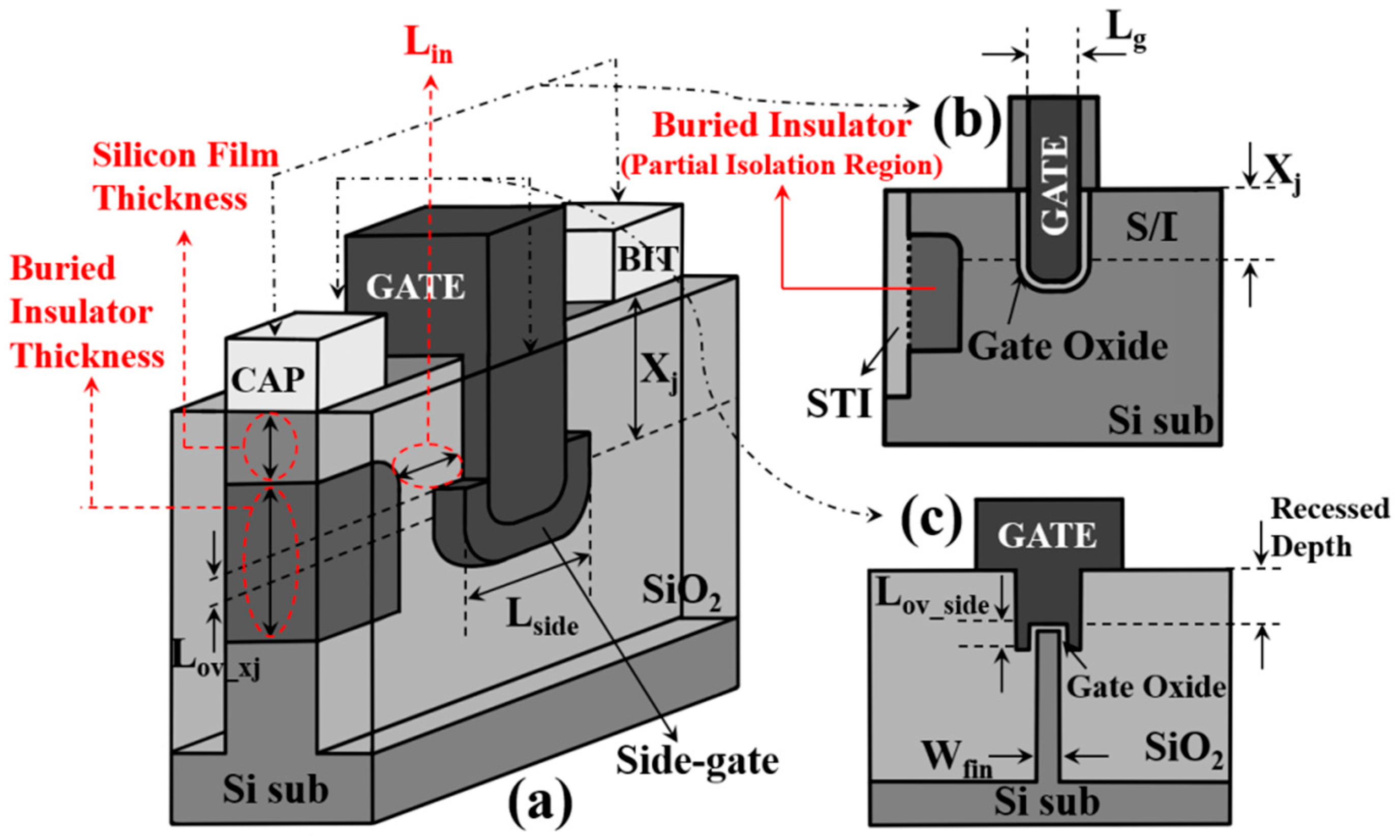
Figure 2.
IDS-VGS characteristic for S-FinFET, RFinFET, Pi-FinFETs, and RCAT at VDS = 1.5 V. Ioff(S-FinFET) = 1.62 × 10⁻¹³ A, Ioff(RFinFET) = 7.80 × 10⁻¹⁵ A, Ioff.Pi-SFinFET = 5.19 × 10⁻¹⁴ A, Ioff.RFinFET = 1.92 × 10⁻¹⁵ A at VGS of −0.5 V.
Figure 2.
IDS-VGS characteristic for S-FinFET, RFinFET, Pi-FinFETs, and RCAT at VDS = 1.5 V. Ioff(S-FinFET) = 1.62 × 10⁻¹³ A, Ioff(RFinFET) = 7.80 × 10⁻¹⁵ A, Ioff.Pi-SFinFET = 5.19 × 10⁻¹⁴ A, Ioff.RFinFET = 1.92 × 10⁻¹⁵ A at VGS of −0.5 V.
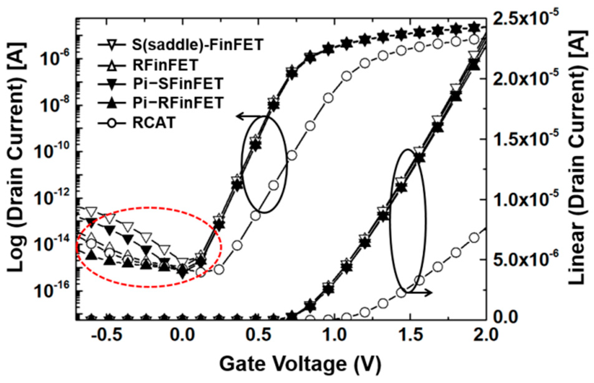
Figure 3.
Potential contour indicating equipotential line distribution near the drain region at VDS = 1.5 V, VGS = −0.5 V. (a) Conventional S-FinFET, (b) Pi-FinFET. Dotted arrows indicate potential drop width (PDW) from 1.8 V to −0.4 V, while dotted red ellipse shows wider PDW compared to conventional S-FinFET.

Figure 4.
(a) Ion, Ioff and (b) drain-induced barrier lowering (DIBL), subthreshold slope (SS) characteristics of Pi-RFinFET and Pi-FinFET according to the ratio of Lin to Lg when Lg is 30 nm.
Figure 4.
(a) Ion, Ioff and (b) drain-induced barrier lowering (DIBL), subthreshold slope (SS) characteristics of Pi-RFinFET and Pi-FinFET according to the ratio of Lin to Lg when Lg is 30 nm.

Figure 5.
(a) Ioff (VGS = −0.5 V, VDS = 1.5 V) and (b) DIBL (VDS.low = 0.05 V, VDS.high = 1.5 V) dependence on Lg of conventional S-FinFETs and Pi-FinFETs.
Figure 5.
(a) Ioff (VGS = −0.5 V, VDS = 1.5 V) and (b) DIBL (VDS.low = 0.05 V, VDS.high = 1.5 V) dependence on Lg of conventional S-FinFETs and Pi-FinFETs.
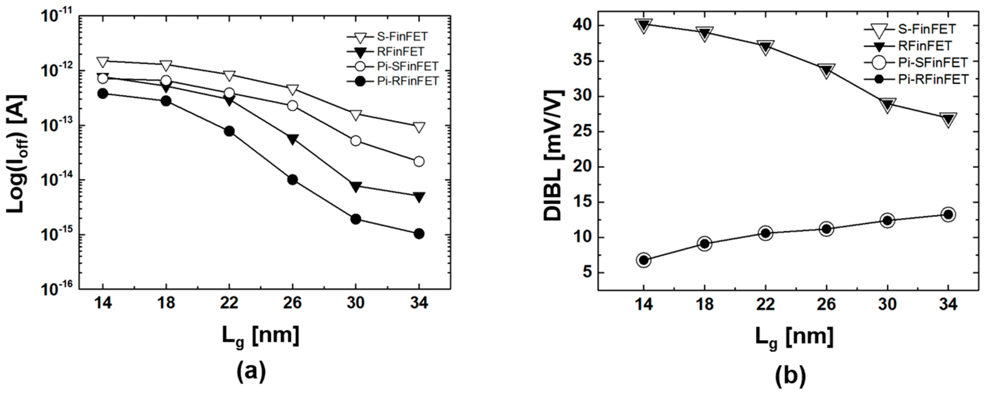
Figure 6.
DIBL (VDS.low = 0.05 V, VDS.high = 1.5 V) and gm.max characteristics of Pi-FinFETs and S-FinFET according to the recessed depth when Lg is 30 nm.
Figure 6.
DIBL (VDS.low = 0.05 V, VDS.high = 1.5 V) and gm.max characteristics of Pi-FinFETs and S-FinFET according to the recessed depth when Lg is 30 nm.

© 2018 by the authors. Licensee MDPI, Basel, Switzerland. This article is an open access article distributed under the terms and conditions of the Creative Commons Attribution (CC BY) license (http://creativecommons.org/licenses/by/4.0/).
Share and Cite
MDPI and ACS Style
Kim, Y.K.; Lee, J.S.; Kim, G.; Park, T.; Kim, H.J.; Cho, Y.P.; Park, Y.J.; Lee, M.J. Partial Isolation Type Saddle-FinFET(Pi-FinFET) for Sub-30 nm DRAM Cell Transistors. Electronics 2019, 8, 8. https://doi.org/10.3390/electronics8010008
AMA Style
Kim YK, Lee JS, Kim G, Park T, Kim HJ, Cho YP, Park YJ, Lee MJ. Partial Isolation Type Saddle-FinFET(Pi-FinFET) for Sub-30 nm DRAM Cell Transistors. Electronics. 2019; 8(1):8. https://doi.org/10.3390/electronics8010008
Chicago/Turabian StyleKim, Young Kwon, Jin Sung Lee, Geon Kim, Taesik Park, Hui Jung Kim, Young Pyo Cho, Young June Park, and Myoung Jin Lee. 2019. "Partial Isolation Type Saddle-FinFET(Pi-FinFET) for Sub-30 nm DRAM Cell Transistors" Electronics 8, no. 1: 8. https://doi.org/10.3390/electronics8010008
Note that from the first issue of 2016, this journal uses article numbers instead of page numbers. See further details here.