Article

A Ku-Band Circularly Polarized Array Antenna Based on Vertical Virtual Ground

1
School of Computer and Communication Engineering, University of Science and Technology Beijing, Beijing 100083, China
2
Shunde Innovation School, University of Science and Technology Beijing, Foshan 528000, China
*
Author to whom correspondence should be addressed.
Electronics 2025, 14(23), 4691; https://doi.org/10.3390/electronics14234691
Submission received: 19 October 2025 / Revised: 17 November 2025 / Accepted: 26 November 2025 / Published: 28 November 2025

Abstract

In this paper, a compact 2 × 2 wideband circularly polarized (CP) array antenna is proposed. The antenna element comprises a square ring resonator, a square parasitic patch, and a vertical virtual ground (VVG) structure. To achieve circular polarization, truncated corners are etched on both the resonator and the parasitic patch; meanwhile, the VVG structure is introduced to enhance miniaturization and improve circular polarization performance. The operating mechanism of the proposed antenna element is analyzed in detail. Furthermore, a one-to-four microstrip power divider is designed to feed a 2 × 2 array, which occupies an area of 1.07λ02. For verification, the 2 × 2 array has been fabricated and measured. The measured results indicate that the proposed antenna operates at a center frequency of 17.2 GHz with a bandwidth of 14.4%. Additionally, it exhibits a 3 dB axial ratio bandwidth of 6.52% and a maximum gain of 8.64 dBi. With excellent CP performance and compact size, the proposed CP array is an attractive candidate for high-resolution radar and satellite communications.

1. Introduction

The Ku-band antennas have been widely employed in satellite communication systems [1,2] owing to their advantages of compact size and high gain. Compared with linearly polarized (LP) antennas, circularly polarized (CP) antennas offer enhanced communication performance due to their ability to suppress multipath interference, immunity to Faraday rotation, and flexibility in orientation between transmitting and receiving antennas [3,4,5].
Various CP antenna structures have been proposed, including dielectric resonator antennas (DRAs) [6] and magneto-electric (ME) dipole antennas [7,8]. However, these configurations typically exhibit a relatively high profile, which limits their suitability for low-profile applications. In contrast, microstrip antennas have been widely adopted in CP designs owing to their compact structure, low cost, and ease of integration with planar circuits [9]. Nevertheless, conventional CP microstrip patch antennas usually suffer from narrow impedance and axial ratio bandwidths [10], which constrains their application in wideband satellite communication systems.
To overcome the inherent narrow bandwidth of conventional CP microstrip antennas, several bandwidth enhancement techniques have been proposed. One approach involves etching slots on the radiating patch to excite additional resonant modes [11,12,13,14]. Another effective approach employs parasitic patches to excite the auxiliary CP modes [15,16,17]. Specifically, the 3 dB axial ratio (AR) bandwidth of a circular patch antenna can be effectively enhanced by etching various slot configurations, such as a lateral slot combined with a square slot [11], two pairs of diagonal slots [12], a U-slot with a square annular slot [13], or a single diagonal slot [14]. In addition, the parasitic patches could be adopted to stimulate additional CP modes and improve circular polarization characteristics. For example, parasitic sector-ring patches were proposed and fabricated in [15] to increase the 3 dB AR bandwidth from 1.3% to 3.3%. In [16], a circle-slotted parasitic patch placed above the radiating patch improved both the AR and the antenna gain. Similarly, in [17], four crown-shaped parasitic patches combined with a slotted ground plane enabled the antenna to achieve broadband circular polarization.
In addition to single-element techniques, array configurations have been widely employed to further increase the gain of microstrip CP antennas. The feeding networks of such arrays can generally be categorized into series-fed [18,19] and parallel-fed [20,21,22] types. Series-fed arrays offer a simple feeding network design, whereas parallel-fed arrays provide greater flexibility in the arrangement of the feeding network. Specifically, a conformal series-fed CP antenna array was reported in [18], achieving a 3 dB axial ratio bandwidth of 4%. Compared with series feeding, parallel feeding offers greater flexibility in feeding network design. In [21], a parallel-fed 1 × 8 microstrip antenna array based on a substrate integrated waveguide (SIW) was designed and analyzed, achieving an operating bandwidth of 3.9%. In [22], a one-to-six power divider was employed to develop a hexagonal aperture-coupled CP microstrip antenna array, yielding a 3 dB axial ratio bandwidth of 4.8%. However, the bandwidths achieved in [18,21] and [22] remain relatively narrow. To further broaden the operating bandwidth, a series-fed array employing six curved phase-shifting transmission lines was proposed in [19], which achieved a 3 dB axial ratio bandwidth of 6.57%.
In this article, a low-profile circularly polarized (CP) microstrip array antenna operating in the Ku-band is presented. The antenna element is implemented on a two-layer substrate, comprising a square-ring radiating patch, a corner-truncated square parasitic patch, and a vertical virtual ground (VVG) structure. Unlike conventional designs [19,21] where metallic vias form SIW cavities, the vias here function as a VVG, confining the electric field, increasing the equivalent electrical length, and enhancing capacitive coupling. This enables a significant reduction in the resonant frequency without increasing the antenna size. In previous works [15,20], CP antennas typically employ a corner-truncated rectangular patch surrounded by multiple parasitic elements. Such layouts lead to relatively large overall dimensions. In contrast, the proposed design adopts a square-ring radiator with corner-truncated parasitic patches vertically stacked above it. This arrangement strengthens the electromagnetic coupling between the radiator and parasitic patches, enhancing circular polarization performance. At the same time, it enables a more compact configuration compared with conventional surrounding-parasitic layouts, facilitating antenna miniaturization.
The main contributions of this work are as follows.
(a)
A VVG-enabled antenna element that reduces the resonant frequency without increasing size;
(b)
Enhanced circular polarization achieved via strong coupling between the square-ring radiator and stacked parasitic patch;
(c)
A practical low-profile Ku-band CP array with validated impedance and axial-ratio performance suitable for compact satellite communications.

2. The Design of the Antenna Element

2.1. Element Structure

The structure of the proposed circularly polarized antenna element is illustrated in Figure 1. The antenna element is designed on a two-layer substrate that comprises a radiating patch, a parasitic patch, and a VVG structure. The two-layer structure is fabricated with TACONIC TLY-5 (Beijing, China) substrate, which has a dielectric constant of 2.2 and a loss tangent of 0.0009. The radiating patch is a square ring resonator with truncated corners, which is fed by a cylindrical coaxial cable. A square parasitic patch with truncated corners is placed above the radiating patch to enhance circular polarization performance. Moreover, metallized vias are arranged along the edges of the two-layer substrate to form a VVG structure, which effectively realize the miniaturization of the antenna element. Compared with alternative approaches such as embedded metal posts or plated through-holes with dielectric filling, the via structure is fully compatible with standard printed circuit board (PCB) and low-temperature co-fired ceramic (LTCC) fabrication processes, making it easy to integrate, cost-effective, and highly reliable. In addition, the via array can be precisely controlled in position and diameter, ensuring the stable vertical current conduction, which is essential for the virtual ground. The design and simulation of this work are carried out with the commercial full-wave electromagnetic solver Ansys HFSS 2020 R1. This software is based on the finite element method (FEM) and provides accurate modeling of complex three-dimensional antenna structures.

2.2. VVG Structure

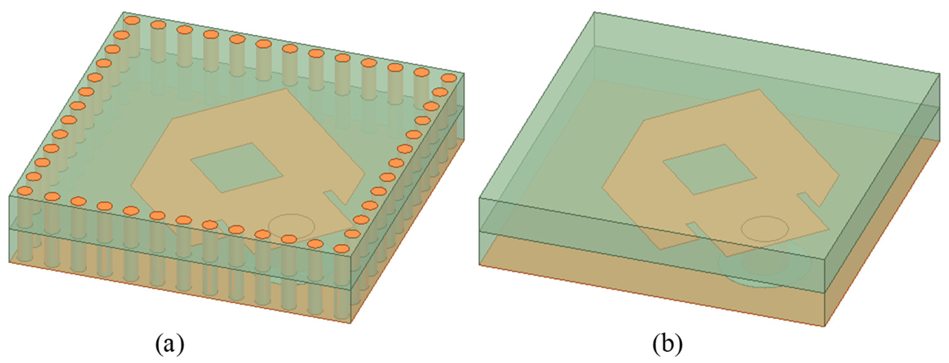
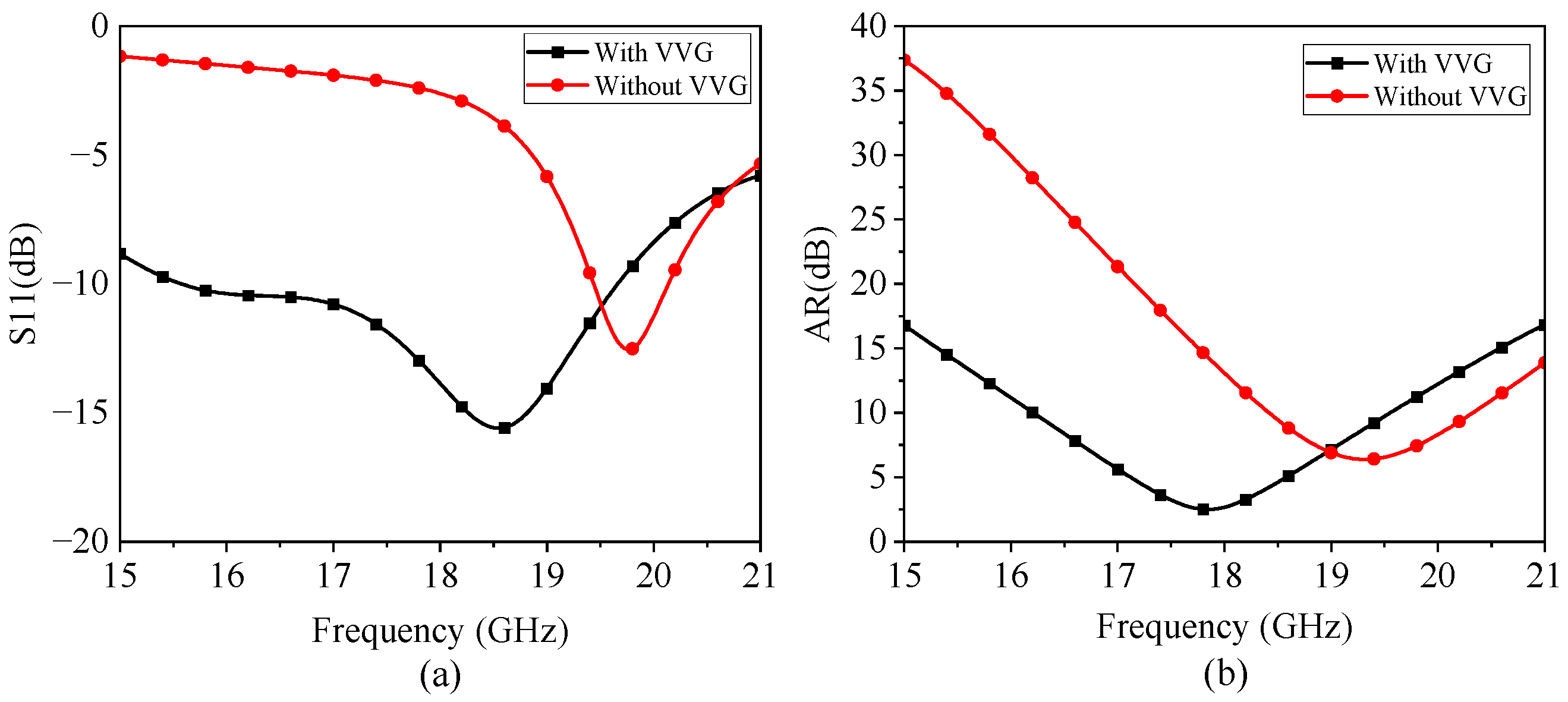
As shown in Figure 2a, the VVG structure is introduced by arranging a series of metal vias around the antenna patch. The VVG structure is composed of the metallic via array that connects the upper substrate to the ground plane. By introducing the VVG, the effective ground plane is extended through these vertical vias. This VVG structure enhances the confinement of the electric field between the patch and the ground, which increases the equivalent electrical length and strengthens the capacitive effect. As a result, the resonant frequency was effectively reduced by introducing VVG. Therefore, the antenna can achieve the same operating frequency with a smaller patch size, leading to a more compact overall design. Subsequently, the antenna elements with and without the VVG structure were simulated, and the corresponding return losses and axial ratios are shown in Figure 3. Accordingly, by adopting the VVG structure, the resonant frequency shifts to a lower frequency, while the bandwidths of the −10 dB impedance matching and 3 dB axial ratio are significantly improved. As verified by simulation, the VVG structure accomplishes the miniaturization and wide operating band of the antenna element.

2.3. Radiating Patch Structure

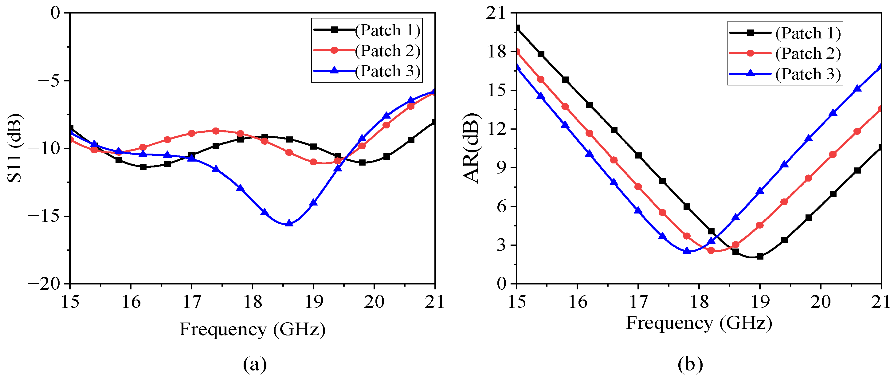
As shown in Figure 4, three different radiating patch configurations are implemented in the antenna element, and their corresponding impedance matching and axial ratio characteristics are presented in Figure 5. In Patch 1, a corner-truncated square patch is fed by a microstrip line to achieve circular polarization. The truncated corners generate two orthogonal current components at the patch edges, enabling initial circular polarization. In Patch 2, a square slot is etched at the center of the patch to lengthen the resonant current path, thereby lowering the resonant frequency. Patch 3 introduces rectangular notches at the interface between the patch and the microstrip line to form an inset-fed structure, which further improves impedance matching. Compared with Patch 1 and Patch 2, Patch 3 achieves improved impedance matching and enhanced circular polarization performance due to the combined effects of the square slot and the inset-fed structure.

2.4. Parasitic Patch Structure

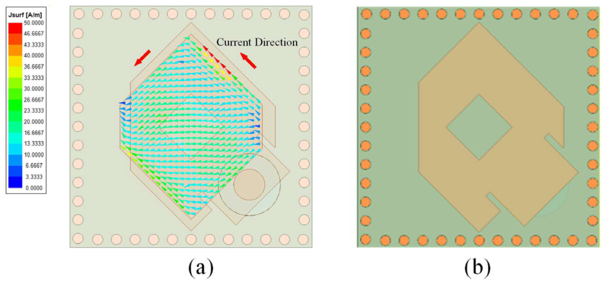
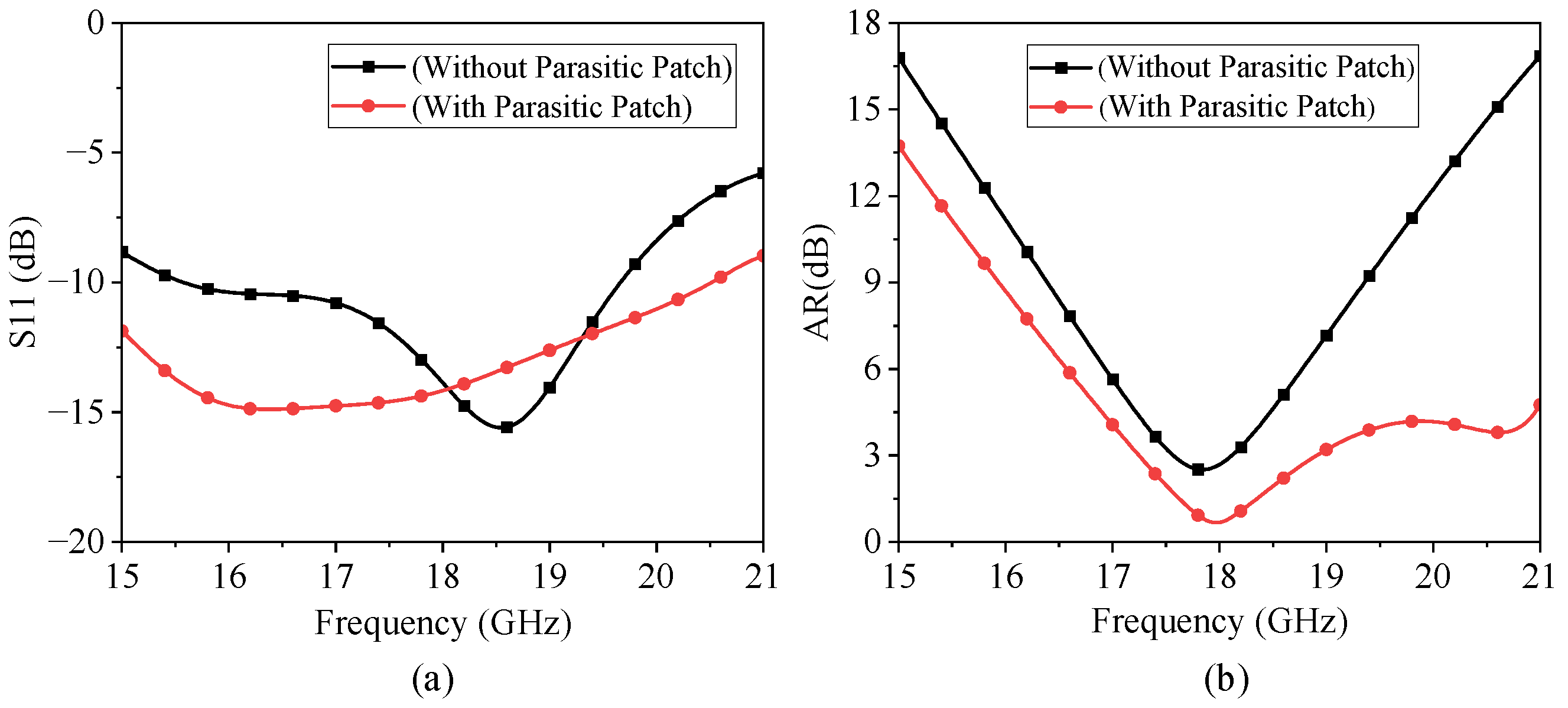
As presented in Figure 6, a square patch with truncated corners is placed above the radiating patch as the parasitic patch. Figure 6a indicates that the surface current of the radiating patch excites the parasitic patch to generate an induced current through electromagnetic coupling after introducing the parasitic patch. Thus, the spatial distribution of the surface current expands from the single radiating patch to the composite structure formed by the radiating patch and the parasitic patch. The multi-mode coupling effect formed by the current of the composite structure enables the antenna to obtain two polarization components with a phase difference stably around 90° and amplitudes approaching equality over a wider frequency range, which reduces the axial ratio and achieves a significant expansion of the axial ratio bandwidth. Additionally, the coupling effect modifies the input impedance characteristics of the antenna, endowing the antenna element with richer current resonance modes. The resonance frequencies of these modes overlap with each other, ultimately resulting in a remarkable improvement in the impedance bandwidth. The frequency responses of the antenna element with and without a parasitic patch are plotted in Figure 7. Accordingly, by employing the parasitic patch, the impedance bandwidth and the axial ratio performance of the antenna element could be effectively improved.

3. The Operating Mechanism of Critical Parameter

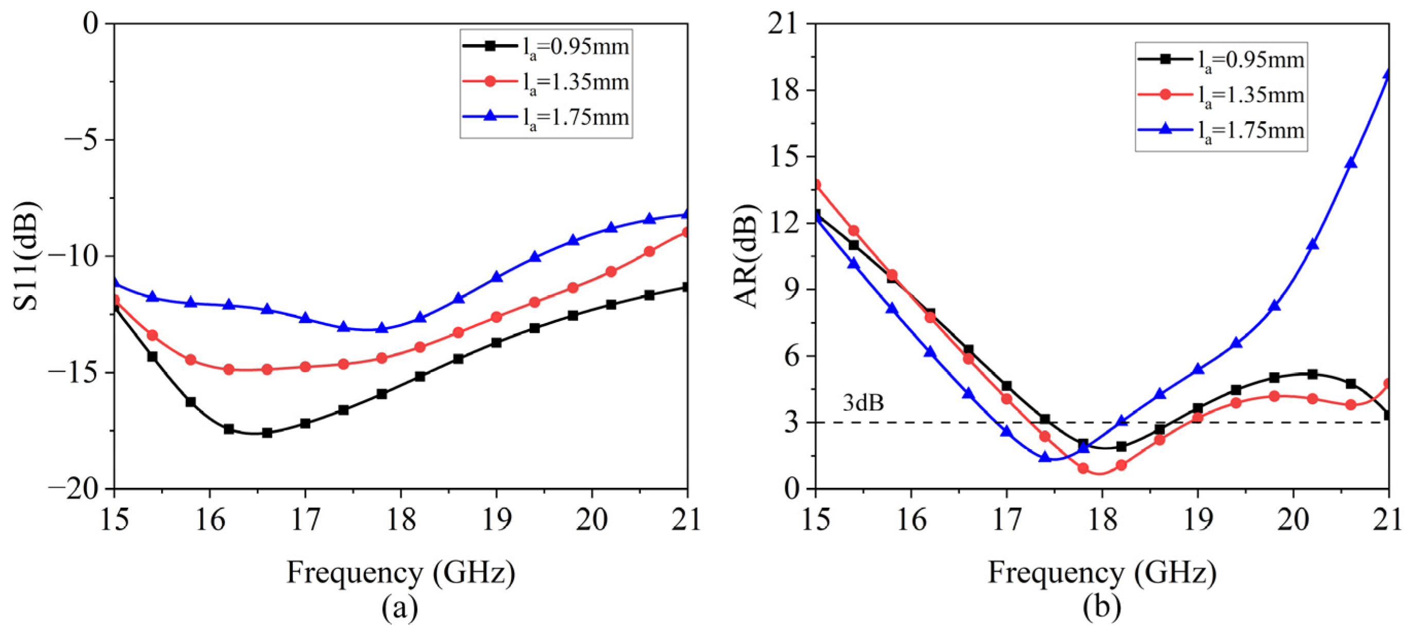
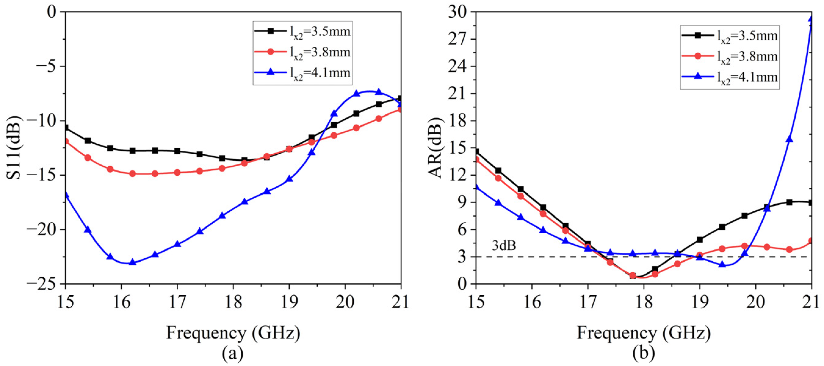
The change in critical dimensional parameters will affect the impedance matching and circular polarization performance of the antenna element. Simulations and analyses are systematically performed to examine the impacts of three key geometric parameters: the side length of the square slot on the radiating patch ( l a ), the side length of the parasitic patch ( l x 2 ), and the truncated-corner width of the parasitic patch ( d s s ).
Figure 8 illustrates the effects of the side length l a of the square slot on the radiating patch on the return loss and axial ratio. It is demonstrated that the resonant frequency of the element increases with the enhancement of l a , accompanied by an increased S11 parameter. The optimal value for this parameter can be determined by considering the situations in which the central axial ratio reaches its minimum value. In this design, the values of 1.35 mm for l a are selected.
The simulated frequency responses of the proposed element with different parasitic patch side lengths l x 2 are shown in Figure 9. It can be observed that impedance matching performance is improved with the increase of l x 2 . When l x 2 = 3.8 mm, the antenna achieves the lowest axial ratio and the widest 3 dB axial ratio bandwidth.
The optimization procedure for the truncated corners width d s s of the parasitic patch is shown in Figure 10. The resonance frequency and impedance matching degree of the antenna both increase with the increment of d s s . The value 0.69 mm for d s s is selected so that the central axial ratio is minimized.

4. The Design of the Antenna Array

4.1. 2 × 2 Array

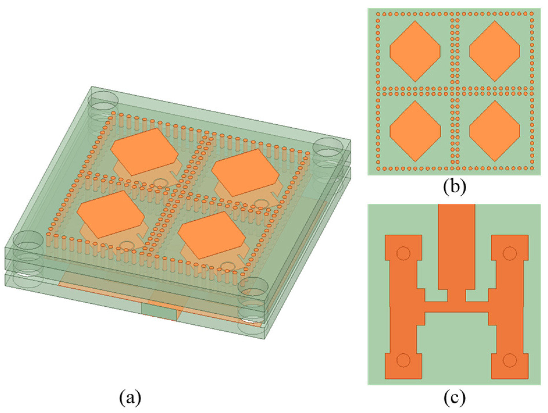
As shown in Figure 11, the proposed circularly polarized array antenna consists of two layers fabricated with TLY-5 substrates: a radiating layer and a feeding layer, with thicknesses of 1.524 mm and 0.762 mm, respectively. The two layers are mechanically connected and electromagnetically transmitted through four cylindrical coaxial cables, which enable the feeding of the radiating elements. Specifically, in the radiating layer, four antenna elements are arranged in a 2 × 2 array configuration, and each element is individually isolated by a VVG structure composed of metallized vias. The element spacing is set to 0.4λ0 (corresponding to 7 mm at the center frequency of 17.2 GHz), effectively suppressing mutual coupling and enhancing array performance. Meanwhile, the feeding layer incorporates a one-to-four microstrip power divider, as illustrated in Figure 11c, which serves as the feeding network to provide equal-phase and equal-amplitude excitation for each radiating element.
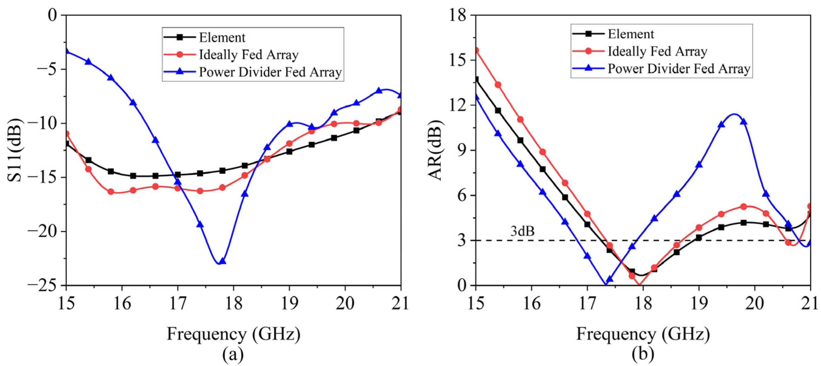
As illustrated in Figure 12, the S11 and axial ratios of the antenna element, 2 × 2 ideally fed array, and the 2 × 2 array fed by a 1-to-4 power divider are compared. The −10 dB S11 and 3 dB axial ratio bandwidths of the proposed element and the ideally fed antenna array are nearly identical, indicating that the mutual coupling between elements in the array exhibits a negligible impact on the circular polarization performance. Accordingly, the narrower axial ratio bandwidth observed in the practical array mainly results from the non-ideal performance of the feeding network. In practice, the 1-to-4 power divider cannot maintain perfectly equal amplitude and phase across the entire operating band, which leads to phase imbalance among the array elements. This imbalance degrades the axial ratio bandwidth of the 2 × 2 array. Meanwhile, when the antenna array is fed by the power divider, the −10 dB S11 bandwidth is reduced to nearly 2 GHz. This is attributed to the limitation of the relative operating bandwidth of the adopted 1-to-4 T-type power divider.

4.2. 4 × 4 Array and 8 × 8 Array

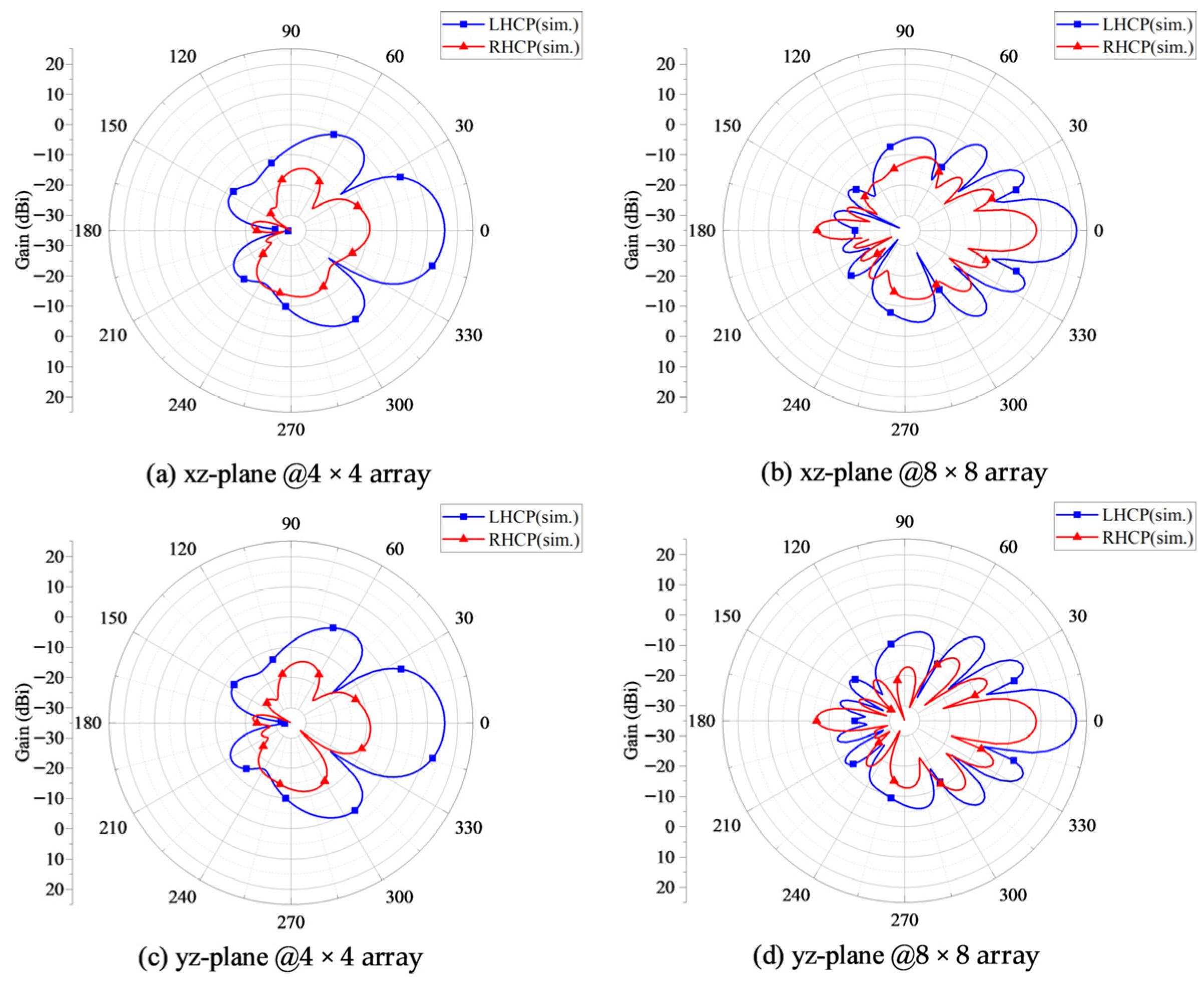
We further simulated the performance of 4 × 4 and 8 × 8 arrays based on the proposed antenna element. The simulated radiation patterns at 18 GHz are shown in Figure 13. Both arrays exhibit left-hand circularly polarized radiation with high gain and excellent polarization purity. The peak gains are 15.71 dBi for the 4 × 4 array and 21.67 dBi for the 8 × 8 array. These results demonstrate that the proposed concept can be effectively scaled to larger array configurations.

5. Measurement and Discussion

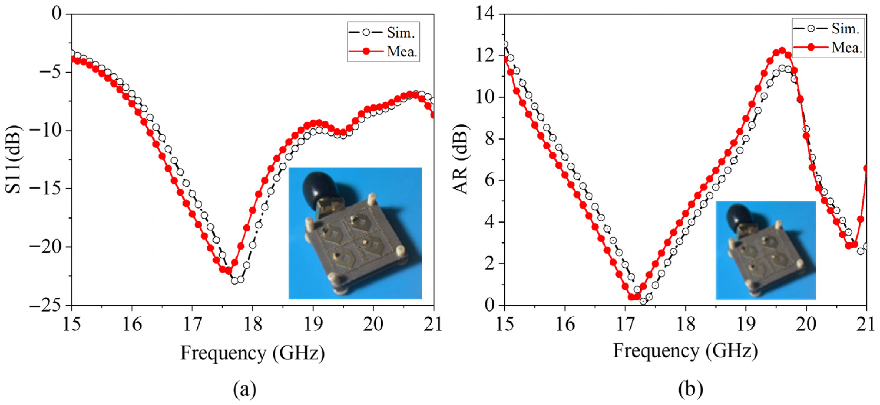
To verify the presented concept, the 2 × 2 circularly polarized array antenna has been fabricated and measured. The dimensional parameters of the proposed antenna are shown in Table 1. The array antenna is measured with a Keysight N5222B vector network analyzer (Keysight Technologies, Beijing, China) in the SATIMO near-field anechoic chamber (StarLab system, Microwave Vision Group (MVG), Beijing, China). Moreover, the corresponding simulated and measured results are presented in Figure 14. As observed from Figure 14, the measured S-parameter and axial ratio agree well with the simulated results. The measured S11 is better than −10 dB, ranging from 16.28 GHz to 18.80 GHz (14.4%), and the measured axial ratio is better than 3 dB, ranging from 16.60 GHz to 17.72 GHz (6.52%).
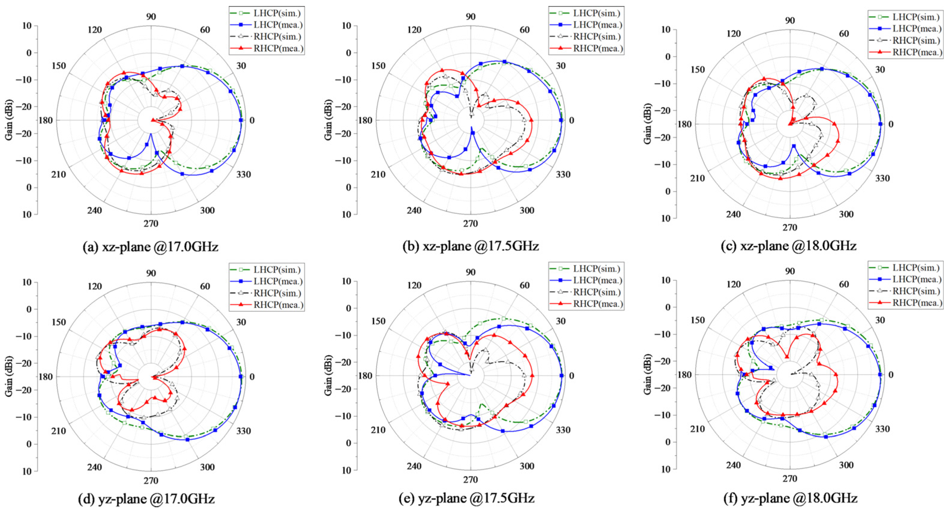
The measured and simulated radiation patterns at 17, 17.5, and 18 GHz in both orthogonal elevation planes are presented in Figure 15. Good agreement is observed between the measured and simulated radiation patterns. As expected, the proposed antenna achieves broadside left-hand circularly polarized radiation with the measured peak gain of 8.64 dBi. The difference between copolarization and cross polarization is greater than 10.9 dBi in the broadside direction in all of the measured radiation patterns, indicating excellent polarization purity. At phi = 0°, the measured front-to-back ratio (FBR) values are 15.95, 17.56, and 18.68 dBi at 17, 17.5, and 18 GHz, with corresponding half-power beamwidth (HPBW) values of 60°, 59°, and 57°, respectively. At phi = 90°, the measured FBR values are 15.79, 16.40, and 20.50 dBi, while the HPBW values are 66°, 63°, and 60°, respectively. These results indicate that the proposed antenna exhibits stable radiation performance across the operating frequency band and at different observation angles. The slight discrepancies between the measured and simulated S-parameters, axial ratio, and radiation patterns in these resulting figures may be caused by fabrication tolerances and measured errors.
To evaluate the performance of the proposed array antenna, the comparisons between the proposed array antenna and the related publications are exhibited in Table 2. As observed from Table 2, the proposed antenna has the lowest profile and the second-widest bandwidth of impedance and axial ratio among the published designs [18,19,20,21,22]. In conclusion, the proposed array antenna exhibits excellent circular polarization performance with a low profile and a simple feed network.

6. Conclusions

In this paper, a compact wideband 2 × 2 CP array antenna based on a single-fed configuration is proposed. The antenna element consists of a square ring resonator, a square parasitic patch, and a VVG structure. Specifically, employing the parasitic patch effectively broadens the impedance bandwidth and improves the axial ratio performance, while the VVG structure further enhances miniaturization and circular polarization characteristics. By integrating the antenna elements with a one-to-four microstrip power divider, a 2 × 2 CP array has been fabricated and measured. The simulated and measured results show good agreement, confirming the validity of the proposed design. Owing to its wide bandwidth, compact size, excellent CP performance, and potential scalability, the proposed array antenna shows great potential for applications such as high-resolution radar and Ku-band satellite communications.

Author Contributions

Conceptualization, G.D.; methodology, S.L.; software, Y.Z.; validation, G.D. and S.L.; formal analysis, Y.Z.; investigation, G.D.; resources, G.D.; data curation, Y.Z.; writing—original draft preparation, S.L.; writing—review and editing, G.D.; visualization, S.L.; supervision, G.D.; project administration, G.D.; funding acquisition, G.D. All authors have read and agreed to the published version of the manuscript.

Funding

This work was supported in part by the National Natural Science Foundation of China under Grant 62501045, in part by the Beijing Natural Science Foundation under Grant 4232016, in part by the Basic and Applied Basic Research Foundation of Guangdong Province under Grant 2022A1515110565, and in part by the Fundamental Research Funds for the Central Universities under Grant FRF-GF-25-005.

Data Availability Statement

Data is contained within the article.

Conflicts of Interest

The authors declare no conflicts of interest.

References

  1. Esmail, B.A.F.; Isleifson, D.; Shafai, L. A Ku-Band Compact Offset Cylindrical Reflector Antenna with High Gain for Low-Earth Orbit Sensing Applications. Sensors 2024, 24, 7535. [Google Scholar] [CrossRef]
  2. Malki, M.; Yang, L.; Gómez-García, R. Ku-Band Reflectionless Single- and Dual-Band Bandpass Filters in Groove Gap Waveguide. IEEE Trans. Microw. Theory Tech. 2025, 73, 5813–5827. [Google Scholar] [CrossRef]
  3. Li, J.; Hu, Y.; Xiang, L.; Kong, W.; Hong, W. Broadband Circularly Polarized Magnetoelectric Dipole Antenna and Array for K-Band and Ka-Band Satellite Communications. IEEE Trans. Antennas Propag. 2022, 70, 5907–5912. [Google Scholar] [CrossRef]
  4. Wang, C.; Li, X.-C.; Keezer, D. Differential-Fed Wideband Circularly Polarized SIW Cavity-Backed Slot Antenna Array. Electronics 2025, 14, 2389. [Google Scholar] [CrossRef]
  5. Hui, W.; Guo, Y.; Xie, K.; Zhao, X. Investigation of Circularly Polarized Microstrip Antenna with Tri-Band Polarization Conversion Metamaterials. IEEE Antennas Wirel. Propag. Lett. 2023, 22, 2831–2835. [Google Scholar] [CrossRef]
  6. Hu, Y.; Pan, Y.M.; Di Yang, M. Circularly Polarized MIMO Dielectric Resonator Antenna with Reduced Mutual Coupling. IEEE Trans. Antennas Propag. 2020, 69, 3811–3820. [Google Scholar] [CrossRef]
  7. Tan, Q.; Fan, K.; Yu, W.; Wang, W.; Liu, L.; Luo, G.Q. A Circularly Polarized Magneto-Electric Dipole Antenna Array with Wide AR and Impedance Bandwidth for Millimeter-Wave Applications. IEEE Antennas Wirel. Propag. Lett. 2023, 22, 2250–2254. [Google Scholar] [CrossRef]
  8. Xu, J.; Hong, W.; Jiang, Z.H.; Zhang, H. Low-Cost Millimeter-Wave Circularly Polarized Planar Integrated Magneto-Electric Dipole and Its Arrays with Low-Profile Feeding Structures. IEEE Antennas Wirel. Propag. Lett. 2020, 19, 1400–1404. [Google Scholar] [CrossRef]
  9. Tran, H.-H.; Nguyen, T.T.-L.; Pham, T.D. Circularly Polarized MIMO Antenna Based on Microstrip Patch and Metasurface Structures. Electronics 2023, 12, 384. [Google Scholar] [CrossRef]
  10. Ji, Z.; Sun, G.; Wang, K.; Wong, H.; Yu, Z.; Li, Z.; Wei, C.; Liu, P. A Circularly Polarized Complementary Antenna with Substrate Integrated Coaxial Line Feed for X-Band Applications. Electronics 2024, 13, 785. [Google Scholar] [CrossRef]
  11. Hao, S.-S.; Chen, Q.-Q.; Li, J.-Y.; Xie, J. A High-Gain Circularly Polarized Slotted Patch Antenna. IEEE Antennas Wirel. Propag. Lett. 2020, 19, 1022–1026. [Google Scholar] [CrossRef]
  12. Ray, M.K.; Mandal, K.; Nasimuddin, N. Low-Profile Circularly Polarized Patch Antenna with Wide 3 dB Beamwidth. IEEE Antennas Wirel. Propag. Lett. 2019, 18, 2473–2477. [Google Scholar] [CrossRef]
  13. Cheng, G.; Huang, B.; Huang, Z.; Yang, L. A High-Gain Circularly Polarized Filtering Stacked Patch Antenna. IEEE Antennas Wirel. Propag. Lett. 2023, 22, 995–999. [Google Scholar] [CrossRef]
  14. Wang, J.; Zhang, Y.; Liu, Q.H. A Wideband Circularly Polarized Filtering Antenna Based on Slot-Patch Structure. IEEE Antennas Wirel. Propag. Lett. 2023, 22, 1858–1862. [Google Scholar] [CrossRef]
  15. Lin, J.-F.; Chu, Q.-X. Enhancing Bandwidth of CP Microstrip Antenna by Using Parasitic Patches in Annular Sector Shapes to Control Electric Field Components. IEEE Antennas Wirel. Propag. Lett. 2018, 17, 924–927. [Google Scholar] [CrossRef]
  16. Santosa, C.E.; Sumantyo, J.T.S.; Gao, S.; Ito, K. Broadband Circularly Polarized Microstrip Array Antenna with Curved-truncation and Circle-slotted Parasitic. IEEE Trans. Antennas Propag. 2021, 69, 5524–5533. [Google Scholar] [CrossRef]
  17. Wang, L.; Zhu, Z.; En, Y. Performance Enhancement of Broadband Circularly Polarized Slot–Microstrip Antenna Using Parasitic Elements. IEEE Antennas Wirel. Propag. Lett. 2021, 20, 2255–2259. [Google Scholar] [CrossRef]
  18. Ogurtsov, S.; Koziel, S. A Conformal Circularly Polarized Series-Fed Microstrip Antenna Array Design. IEEE Trans. Antennas Propag. 2020, 68, 873–881. [Google Scholar] [CrossRef]
  19. Yang, Y.H.; Sun, B.H.; Guo, J.L. A Low-cost, Single-layer, Dual circularly Polarized Antenna for Millimeter-wave Applications. IEEE Antennas Wirel. Propag. Lett. 2019, 18, 651–655. [Google Scholar] [CrossRef]
  20. Sadeghi-Marasht, S.; Sharawi, M.S.; Zhu, A. Dual-Band Circularly Polarized Antenna Array for 5G Millimeter-Wave Applications. IEEE Open J. Antennas Propag. 2022, 3, 314–323. [Google Scholar] [CrossRef]
  21. Park, S.-J.; Park, S.-O. LHCP and RHCP Substrate Integrated Waveguide Antenna Arrays for Millimeter-Wave Applications. IEEE Antennas Wirel. Propag. Lett. 2017, 16, 601–604. [Google Scholar] [CrossRef]
  22. Liao, H.; Shamim, A. A Low-Profile and High-Aperture-Efficiency Hexagonal Circularly Polarized Microstrip Antenna Array. IEEE Antennas Wirel. Propag. Lett. 2022, 21, 615–619. [Google Scholar] [CrossRef]
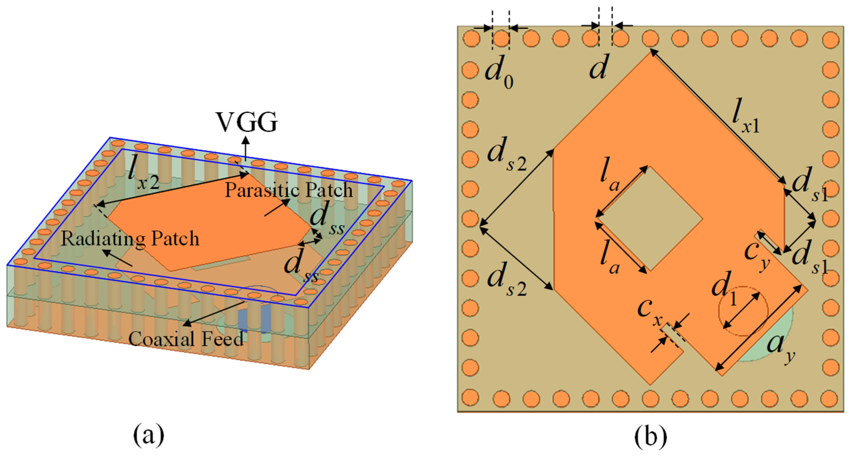
Figure 1. The schematic diagram of the antenna element: (a) 3D view; (b) top view.
Electronics 14 04691 g001
Figure 2. The schematic diagram of the antenna element: (a) with VVG; (b) without VVG.
Electronics 14 04691 g002
Figure 3. Frequency responses of the antenna element with and without VVG: (a) return loss; (b) axial ratio.
Electronics 14 04691 g003
Figure 4. The schematic diagram and surface currents of the radiating patch: (a) Patch 1; (b) Patch 2; (c) Patch 3.
Electronics 14 04691 g004
Figure 5. Frequency responses of the antenna element with three different radiating patch structures: (a) return loss; (b) axial ratio.
Electronics 14 04691 g005
Figure 6. Design procedure of the element structure: (a) with parasitic patch; (b) without parasitic patch.
Electronics 14 04691 g006
Figure 7. Frequency responses of the antenna element with and without a parasitic patch: (a) return loss; (b) axial ratio.
Electronics 14 04691 g007
Figure 8. Frequency responses of the antenna element with different l a : (a) return loss; (b) axial ratio.
Electronics 14 04691 g008
Figure 9. Frequency responses of the antenna element with different l x 2 : (a) return loss; (b) axial ratio.
Electronics 14 04691 g009
Figure 10. Frequency responses of the antenna element with different d s s : (a) return loss; (b) axial ratio.
Electronics 14 04691 g010
Figure 11. Array antenna structure: (a) 3D view; (b) radiating layer; (c) feeding layer.
Electronics 14 04691 g011
Figure 12. Frequency responses of the antenna element, the ideally fed array, and the power divider fed array: (a) return loss; (b) axial ratio.
Electronics 14 04691 g012
Figure 13. Simulated radiation patterns of the antennas with the 4 × 4 array and the 8 × 8 array.
Electronics 14 04691 g013
Figure 14. The simulated and measured results of the 2 × 2 CP antenna array: (a) return loss; (b) axial ratio.
Electronics 14 04691 g014
Figure 15. Measured and simulated radiation patterns of the array antenna.
Electronics 14 04691 g015
Table 1. Dimensional parameters of the antenna unit (mm).
ParametersValueParametersValue
l x 1 3.44 l x 2 3.8
l a 1.35 d s 1 0.84
d s 2 1.8 d s s 0.69
c x 0.18 c y 0.59
d 0 0.3 d 1 0.87
d 0.24 a y 2.2
Table 2. Comparisons between the proposed antenna and previous reported designs.
Antenna TypeFrequency
(GHz)
BWIM
(%)
BWAR
(%)
Size
02)
Gain
(dBi)
HPBW
(°)
FBR
(dB)
[18]Array
(1 × 10)
9.75341.47103018
[19]Array
(1 × 7)
30.1>206.577.811.793525.4
[20]Array
(2 × 2)
285.63.22.7915.6961
[21]Array
(1 × 8)
28.35.53.938.713.09101.6
[22]Array
(1 × 6)
1.563114.81.3812.44238.2
This work Array
(2 × 2)
17.214.46.521.078.646620.5
BWIM: bandwidth of impedance matching, BWAR: bandwidth of axial ratio.
Disclaimer/Publisher’s Note: The statements, opinions and data contained in all publications are solely those of the individual author(s) and contributor(s) and not of MDPI and/or the editor(s). MDPI and/or the editor(s) disclaim responsibility for any injury to people or property resulting from any ideas, methods, instructions or products referred to in the content.