1. Introduction
Integrated thermal sensor (TS) circuits have become key elements in high performance systems, especially in processors and system on chip (SoC). Such applications require a relatively high precision thermal sensor (typically ±3 °C in a wide temperature range), in order to achieve high reliability and performance [
1,
2]. The conventional method of thermal sensing is based on diode connected Bipolar Junction Transistor (BJT) voltage temperature dependence [
2,
3,
4,
5,
6,
7]. A base-emitter voltage equation of BJT transistor is (to first order approximation):
where
n is the ideality factor of the diode,
k is Boltzmann’s constant,
T is the absolute temperature,
q is the electron charge,
I0 is the diode’s saturation current and
I is the current through the diode. This voltage is inversely proportional to the temperature, because of the strong temperature dependence of the saturation current
I0. The diode voltage is marked as
VBE, since a diode connected BJT transistor is used in order to implement a diode, from this point onwards when referring to “diode” the meaning is diode connected BJT.
The differential voltage between the two diodes is:
where
M is the ratio between the diodes’ current density. This voltage is directly proportional to the temperature.
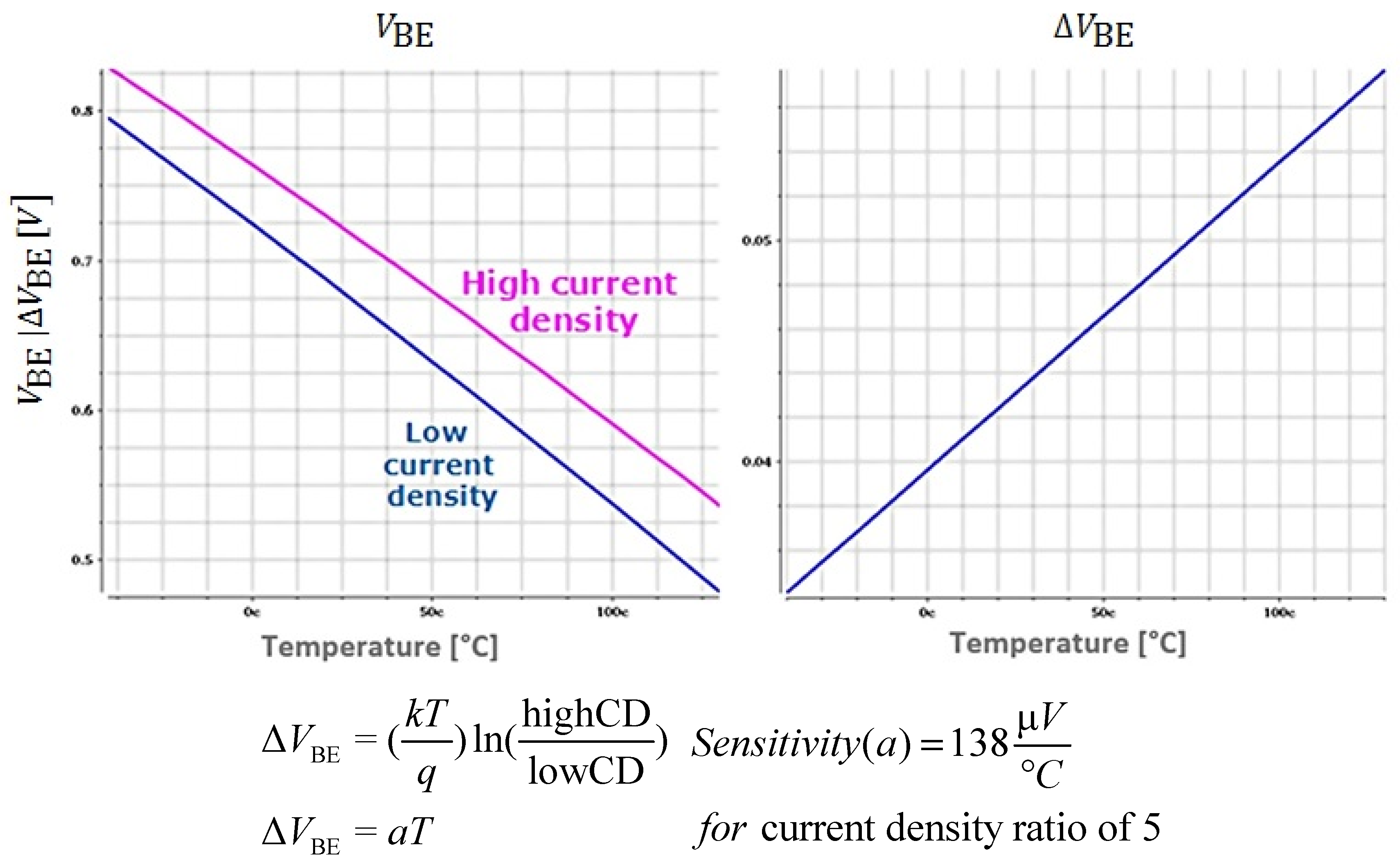
Several methods have previously been used to read out the diodes’ voltage and convert it into a temperature reading. One of the popular implementations, used at industry, finds the crossing point between the amplified differential voltage of the two diodes, which is directly proportional to the temperature, and the voltage of a single diode, which is inversely proportional to the temperature (see
Figure 1) [
8]. For a given temperature, there will be exactly one crossing point, which exists only for a specific diodes’ current. This current is controlled by a Digital to Analog Converter (DAC). A controller sweeps across the current DAC until this point is found by a comparator. The DAC code at this point represents the evaluated temperature [
9]. This architecture is relatively limited in linearity and accuracy over a wide temperature range.
Moreover, there is a variance in the slope of the linear functions, due to sensitivity to process variations. The slope initial variation is large, requiring two-temperature calibration in order to achieve the required accuracy. Performing two temperature calibrations during High Volume Manufacturing (HVM) tests is considered costly.
Several motivations drove and guided the design of the temperature sensor presented in this paper: (a) to provide the best possible accuracy, as accurate temperature sensing extends performance of SoCs; (b) to utilize advanced circuit techniques to overcome process variance effects and, thus, to get a robust and accurate TS; (c) to reduce the products’ HVM calibration process cycle to a single-temperature calibration or to no calibration; (d) to achieve goals (a) and (b) with the smallest possible power and area penalty; and (e) to be configurable in order to meet a wide range of power versus sampling rate optimized envelop for different requirements of several projects.
Figure 1.
Operation principle of thermal sensor (CD—current density; a—temperature coefficient of ΔVBE).
Figure 1.
Operation principle of thermal sensor (CD—current density; a—temperature coefficient of ΔVBE).
2. 22 nm Sigma-Delta Based Thermal Sensor Architecture
Better linearity is achieved using the Analog to Digital Converter (ADC) based thermal sensor [
3,
4]. In this architecture, the differential voltage is amplified and converted into a digital word by an ADC. A bandgap voltage reference circuit (BG) can be used in order to supply a precision reference voltage for the ADC. This operating mode is called Vref mode. Another operating mode is creating the reference voltage internally in the TS. This is referred as Ratiometric mode (
Figure 2). The ADC-based architecture has very good linearity over a wide range of temperatures. The accuracy of this architecture can be improved by using a calibration process during production. This architecture may produce accuracy of better than ±0.5 °C with old processes [
3,
4,
6,
7].
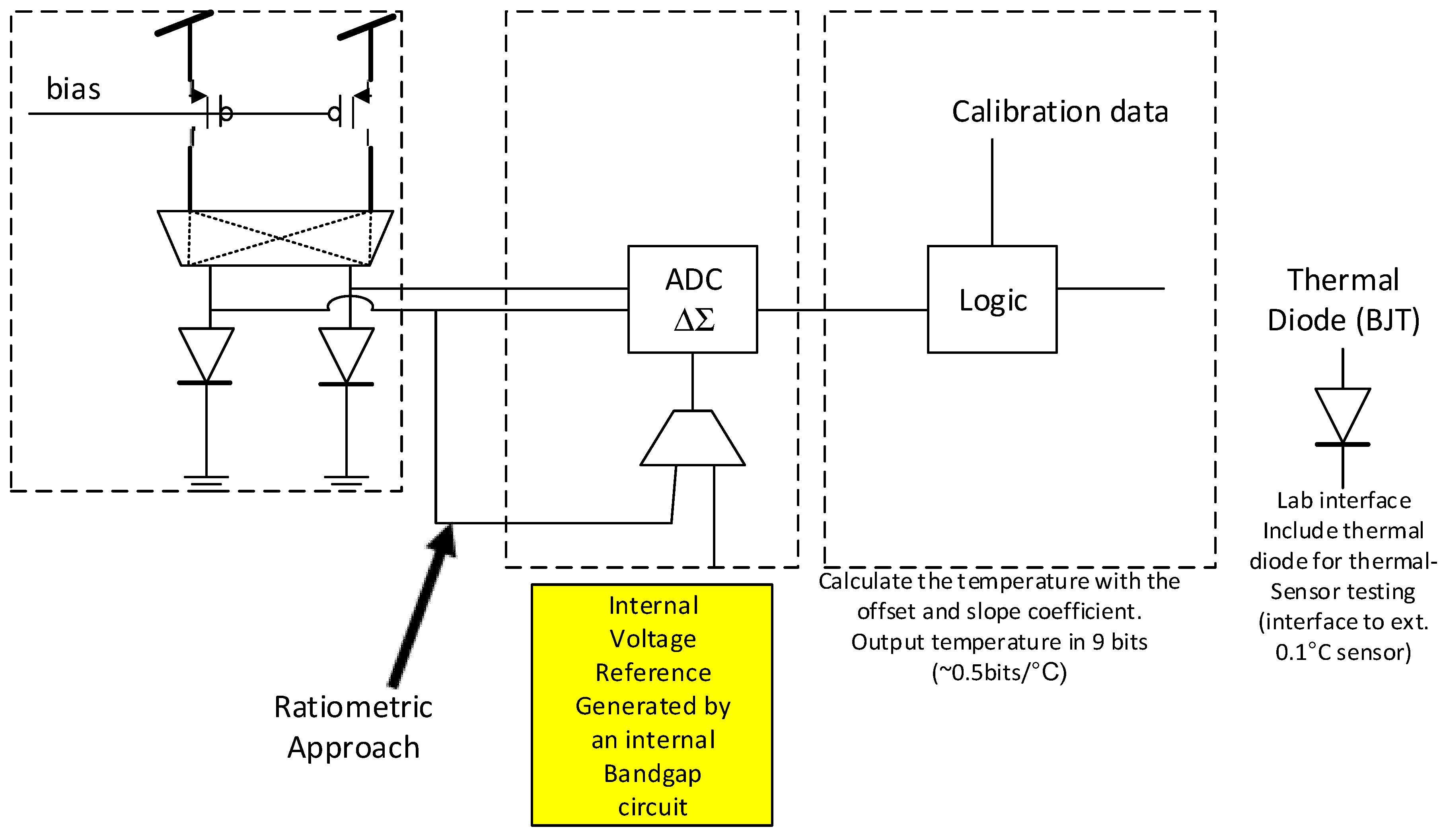
The thermal sensor presented here was fabricated in the 22 nm process. The architecture includes an advanced sense stage combined with circuits that deal with process variations (chopping and dynamic element matching). A second order sigma-delta (SD) ADC is used both as an amplifier and as a converter that translates the temperature readings to a digital word. The SD converter includes correlated double sampling which improves its 1/f attenuation and offset performance and a custom made digital block. A synthesized block implements the sigma-delta decimation filters and provides a digital readout of the relative operating temperature as well as temperature alerts. This sigma-delta ADC based TS can be operated in two modes: Reference-based (Vref) and Ratiometric-based (Ratiometric). In the Ratiometric approach, the converter extracts bandgap voltages directly from the sense stage. Stabilization is achieved by feed-forward methodology. The sigma-delta modes are selectable through digital control manipulation only, without additional analog components. A thermal diode was also included within the TS for junction temperature sensing by a ±1 °C sensor, as part of the calibration process.
The TS has two main power modes: high sampling rate and power saving. In the power saving mode, the TS is switched on for a short time that enables reading of accurate temperature and most of the time the TS is off. In this method, the TS probes the temperature in frequencies of 10 to 100 samples/s . In the high sampling rate mode the TS is continuously working with the sigma-delta modulator clocked at a lower frequency and samples the temperature in frequencies of 5 K to 45 K samples/s.
Figure 2.
High level diagram of the Thermal Sensor.
Figure 2.
High level diagram of the Thermal Sensor.
Device mismatches, such as between current mirrors and between diodes, are effectively treated by the advanced dynamic compensation circuit techniques. However, there are a few errors which require compensation during calibration if an improved accuracy is required. The sources of these errors are process variations of diode parameters, such as the ideality factor, variation of the conversion factor of the ADC dominated by capacitor mismatch, and Bandgap reference voltage variation in Vref mode only. The High Volume Manufacture (HVM) calibration result is stored in on-die fuses for use by the thermal sensor.
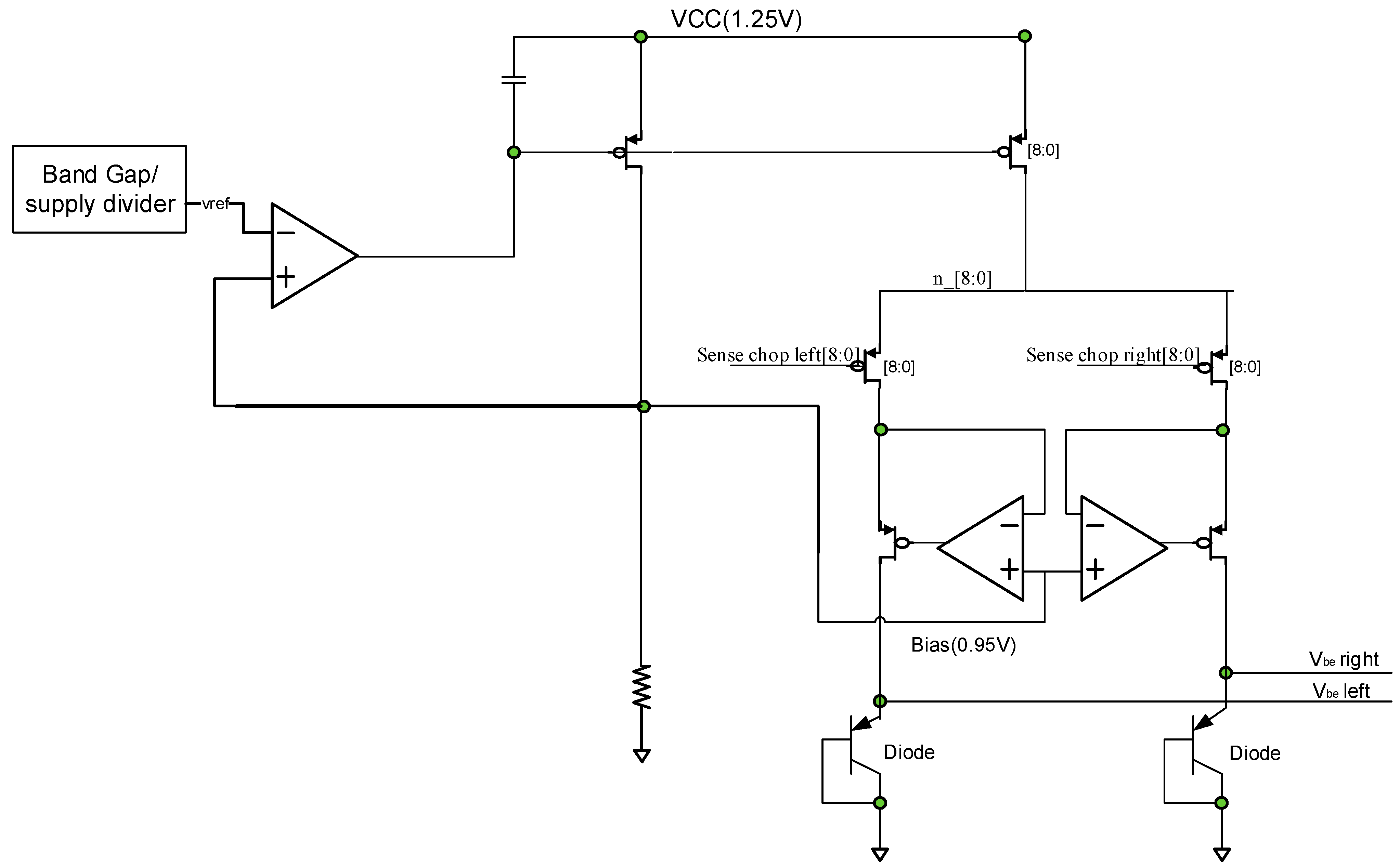
3. The Sense Stage
The sense stage diagram, presented in
Figure 3, converts the junction temperature to a Proportional to Absolute Temperature (PTAT) voltage. It includes a matched pair of diodes and current mirrors with controlled current ratios (of 3.5, 4, 5, 6, 7, and 8). The absolute value of the mirrored current is controlled by an internal resistor and is equal to a reference voltage divided by the resistor value. The absolute current is designed to be a controlled value since it affects the current density within the diodes, thus affecting their performance as thermal sensing elements. In this work, the bias current of a single current source is nominally 15 μA. The current mirrors use gain boosting (regulated cascode) in order to increase current mirror output resistance, Rout, thus, further improves the current accuracy. These circuits paved the way to achieve accurate TS without the need of temperature calibration.
Figure 3.
Sense stage block diagram.
Figure 3.
Sense stage block diagram.
Current ratios are realized by utilizing nine identical current sources and by switching different subsets of the current to either the right or the left diode. In addition, current sources may be switched to a third diode, the waste diode (not shown in the figure), if they are not in use. The waste diode is implemented by driving current into dummies in the matched diode structure, thus avoiding the area penalty of extra circuitry and enable operating of the sense stage in higher frequency.
In order to obtain accurate current ratios resilient to mismatch, Dynamic Element Matching (DEM) is used. The DEM mechanism is realized by cyclically rotating the nine current source connections to the sense diodes and time-averaging the current value of the current mirrors.
Chopping is also used by the sense circuit in order to overcome diode mismatches. After selecting a current ratio, for example 7:2, it may be connected to the diodes in the reverse order as well (e.g., 2:7), thus changing the sign of ΔVBE. This effectively modulates the signal on a carrier frequency, later to be demodulated by the sigma-delta converter. The chopping frequency is identical to the sampling frequency of the sigma-delta ADC so demodulation is back to DC.
From the circuit perspective, the sense stage is implemented with digital transistors on a relatively low power rail (1.25 V). The low threshold voltage of the digital transistors improves the circuits’ headroom and improves the matching and Rout of the current mirrors and aids in achieving a good PSRR and an accurate TS in a small die area.
4. The Sigma-Delta Modulator
The sigma-delta modulator is a second order, one bit, switched-capacitor based design. Switched-capacitor circuits are frequently used for sigma-delta designs because they are fully compatible with digital CMOS processes. For low bandwidth applications, the over-sampling ratio (OSR) may be high enough so as not to limit the resolution of the ADC. A second order modulator is a preferred choice because it greatly reduces the stability problems of higher order modulators and decreases idle tone generation. It also lowers requirements for the OSR and thus for the gain of the integrator amplifiers. Integrator parameters (gains) are defined by the ratio of capacitors which is more accurate than absolute values of RC components in continuous time modulators. To reduce power supply noise and other distortions due to the common mode disturbance, a fully differential topology is chosen.
Correlated double-sampling (CDS) techniques and chopping are further used to decrease offset, 1/f noise and inaccuracy effects within the SD ADC.
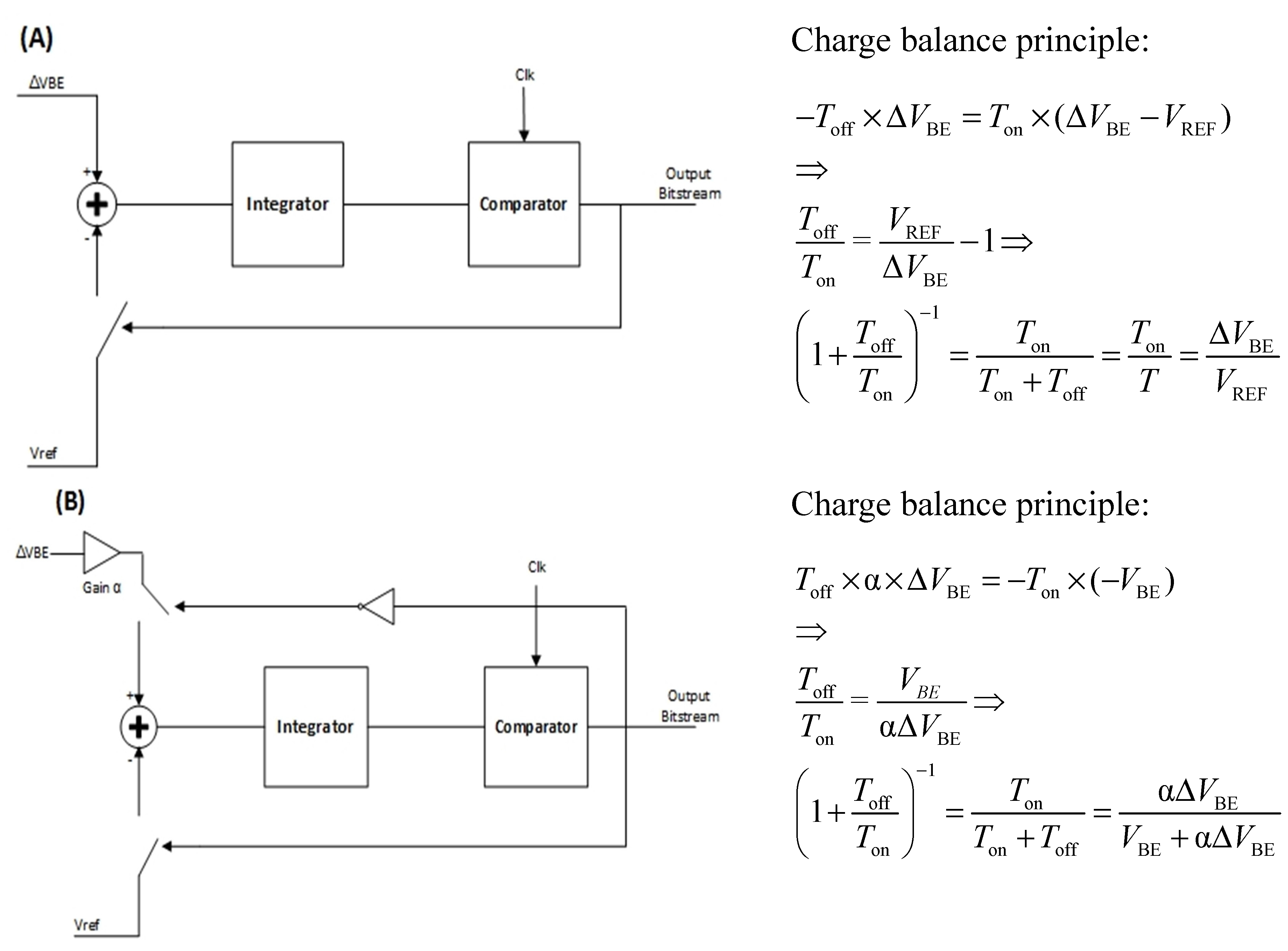
The principles of the sigma-delta operation in the Vref-based and Ratiometric modes are presented in
Figure 4. Charge balance is a fundamental property of any sigma-delta converter. This principle can be used to calculate the average signal transfer function of the modulator. The second stage of the SD-ADC affects mostly the quantization errors and thus does not change the essential transfer function of the ADC.
Figure 4.
Sigma-delta Analog to Digital Converter (ADC) operation principle—(A) Vref mode; and (B) ratiometric mode.
Figure 4.
Sigma-delta Analog to Digital Converter (ADC) operation principle—(A) Vref mode; and (B) ratiometric mode.
Charge-balance mathematics are applied for demonstration to the reference-based sigma-delta, showing how the voltage ratio (ΔVBE/VREF) is converted into an average duty ratio (or “1” density ratio) by the converter.
Applying the same principle to the ratiometric construction shows how the “1” density ratio in the bitstream of the Ratiometric modulator is caused by the ratio:
where α is the preamp gain and Δ
VBE and
VBE are the diodes’ voltages generated by the sense stage. Proper selection of α will cause the denominator to balance the complementary to absolute temperature (CTAT) behavior of
VBE against the proportional to absolute temperature (PTAT) behavior of Δ
VBE, achieving the reference Vref within the sigma-delta converter itself. This phenomena is named Ratiometric sigma-delta [
6,
7], and is used in the thermal sensor in order to omit the bandgap from the sense path (utilizing instead the natural “bandgap” that is already embedded in the sense stage).
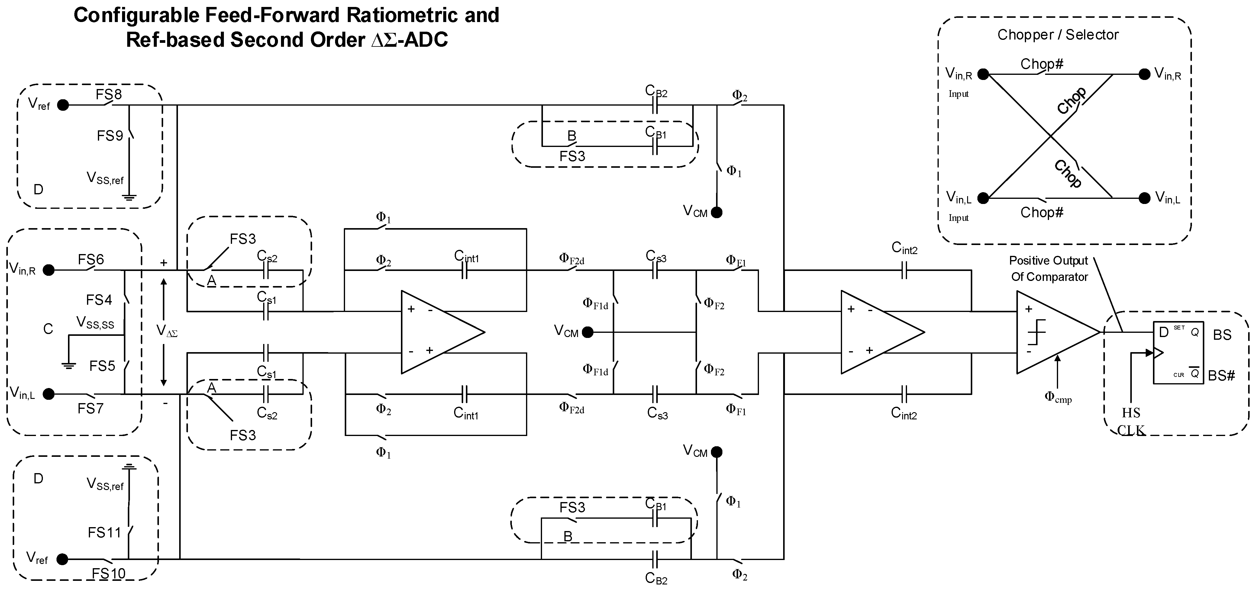
The architecture of the sigma-delta converter is presented in
Figure 5. The architecture is based on the converter presented by Pertijs and al [
7]. Each amplifier constitutes an integrator, thus this circuit is a second order design.
The first integrator incorporates an offset cancelling scheme. It stores the offset on the input capacitors with reverse polarity and during the integration phase the stored offset is subtracted from the integrated signal. The input capacitors to the first amplifier are used to implement a controlled gain. If FS3 is off, then the bucket capacitor of the integrator consists of Cs1 only. Therefore the gain of the integrator would be Cs1/Cint1. However, if Cs2 is connected, the gain would be (Cs1 + Cs2)/Cint1. We use this feature in Vref-mode to boost the ΔVBE signal by a factor of eight, and in the Ratiometric mode as part of the gain α. This eliminates the need for a preamplifier between the sense stage and the ADC converter, thus saving power and area. Additional gain may be obtained, if required, by performing several cycles of integration before the comparator clock (Φcmp) is asserted.
Figure 5.
Second order sigma-delta converter.
Figure 5.
Second order sigma-delta converter.
The second stage is a switch capacitor integrator. Feed-forward path stabilization causes low swing at the opamps’ outputs so less distortion is expected. No DC component above CM voltage exists at the first integrator output. However, the feed-forward method makes the transfer function depend on capacitors’ mismatch.
The ADC is controlled by several clocks (Φ1, Φ1t and Φ2, Φ2t and their delayed versions) and functional switch controls: FS3-FS11. This set of control signals is generated by a custom logic circuit within the ADC, Which selects values for the functional switches in two different modes of operation: Vref-based and Ratiometric-based converters.
The bit stream output feeds a three-stage (CIC) filter that removes high-frequency noise and frames the sampled signal into nine bit samples.
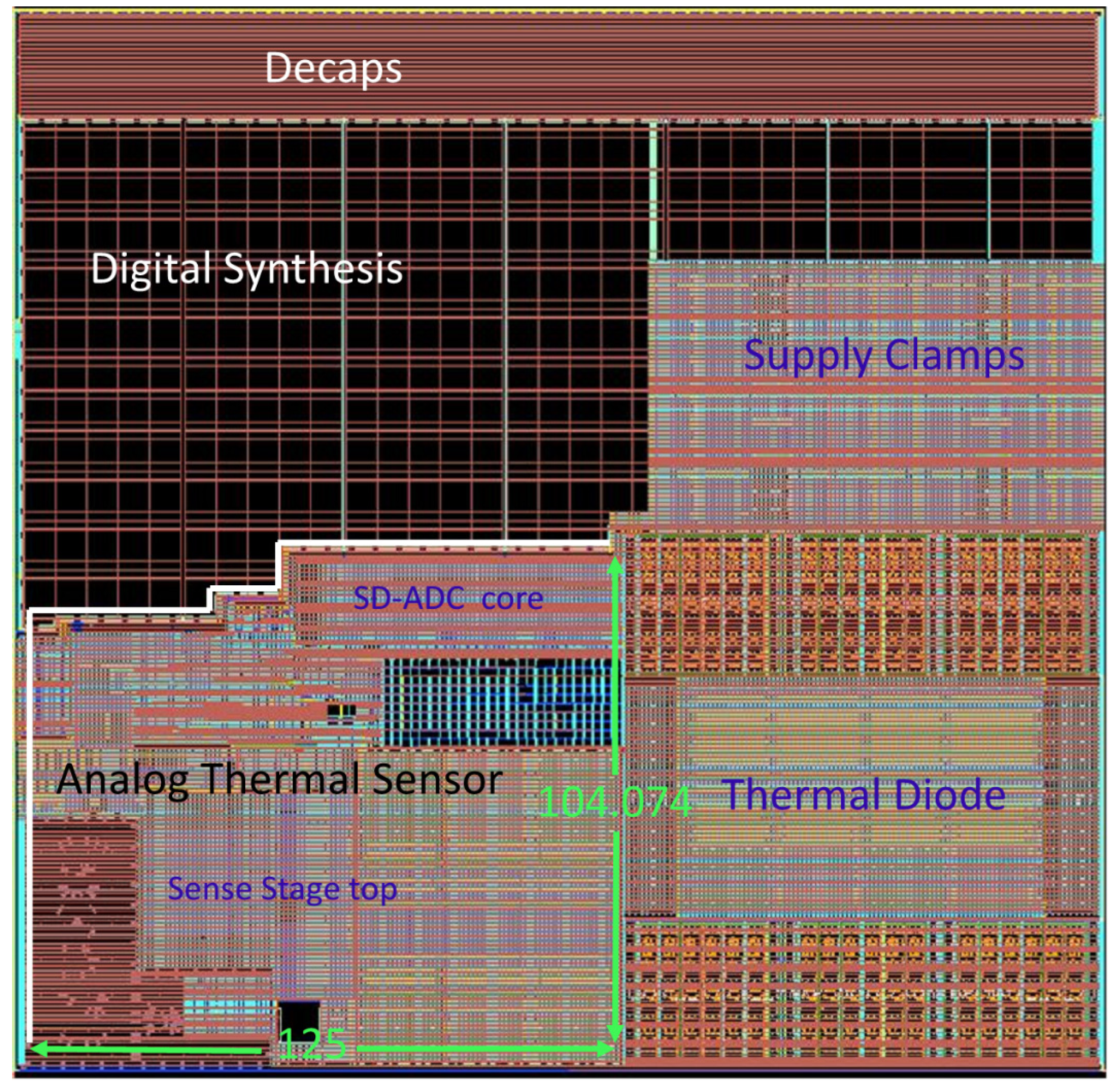
5. The TS Top Hierarchy and Layout
As mentioned above, this TS IP is designed for SoC projects and therefore it is designed as a self-contained collateral that includes all the infrastructure for supporting the requirements of multiple projects. In addition to the TS analog core circuit of 0.013 mm
2, there are other pieces of collateral, including: (1) a thermal diode used in the calibration process; (2) a logic core required for digital DSP, filtering and processing the SD-ADC output; (3) two analog ports for Si testing that are connected directly to critical points in the circuit or through analog to frequency converters (A2F); (4) clamps and decoupling capacitors; and (5) Jtag interface for independent accessibility. The thermal sensor layout picture and specifications are presented in
Figure 6.
Figure 6.
The self-contained thermal sensor layout picture including above the TS core area also thermal diode, clamp, supply decoupling and logic.
Figure 6.
The self-contained thermal sensor layout picture including above the TS core area also thermal diode, clamp, supply decoupling and logic.
The analog core works on a 1.25 V although the digital transistors do not support such direct voltage stress. In order to overcome the over stress limitations of the transistors, advanced techniques were used, such as adding protecting devices and start-up circuits. The use of digital transistor with higher supply voltages enables high bandwidth, relatively high sampling rates, enough headroom range and very small die area. The ADC improved performance together with a configurable and fast digital filter, reduces the latency time of temperature readout, and enables the TS to work with a wide envelope of sample frequencies with optimized power options.
6. Results
The suggested SD-ADC based thermal sensor was implemented in a 22 nm process and was verified in two generations of test chips on typical and skew material. The evaluation boards included an adapter for a thermal head, which forces a specific temperature and an external component for checking the internal thermal diode for measuring the junctional temperature. Extracting the temperature inaccuracy of each chip was done in Ratiometric mode at a temperature range of 0–110 °C.
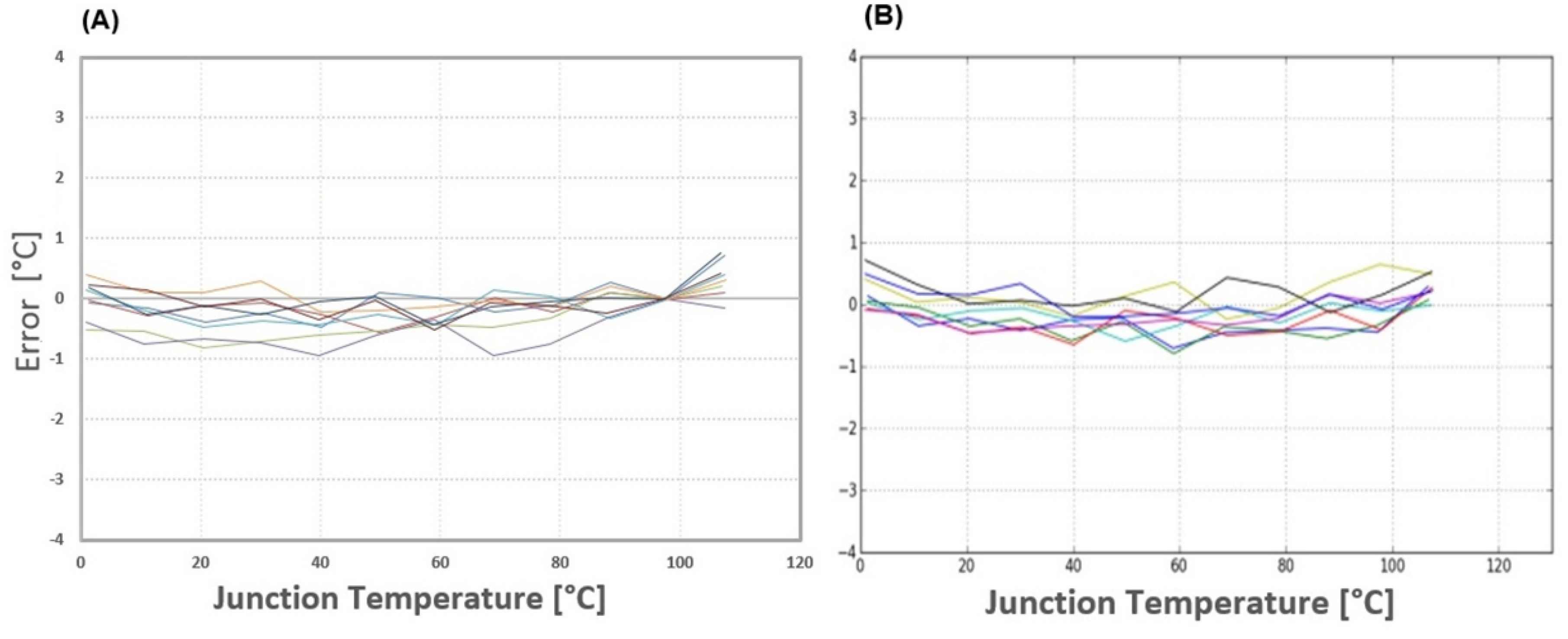
Figure 7A depicts the temperature reading errors of typical dies after one temperature calibration at 100 °C in Ratiometric mode with supply voltage of 1.25 V. The error for a wide range of temperature is smaller than ±1 °C. The results of the same chips only untrimmed (non-calibrated) demonstrates an inaccuracy of smaller than ±1 °C (
Figure 7B). Note that these results include the error induced by the measuring procedure done by the thermal diode.
Figure 7.
Temperature error versus junction temperature of different typical chips: (A) calibrated in one temperature and; (B) untrimmed.
Figure 7.
Temperature error versus junction temperature of different typical chips: (A) calibrated in one temperature and; (B) untrimmed.
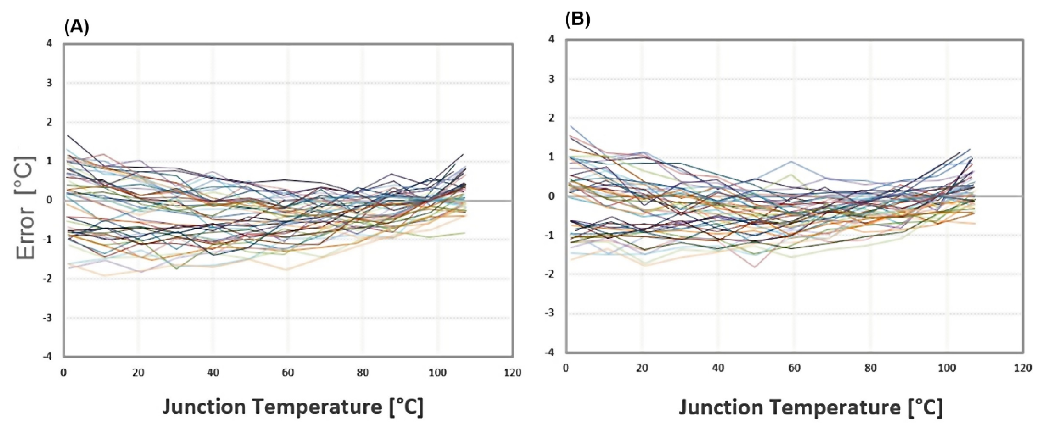
The TS circuit is differential and is very insensitive to power supply variation. The temperature error curves with various supply voltages of 1.25 V ± 5%, and 1.35 V ± 5% are presented in
Figure 8 with an inaccuracy of smaller than ±1.8 °C demonstrating a good immunity to supply voltage. In addition, simulations support these results and demonstrate a high PSRR of >50 dB for the Δ
VBE signal over a wide frequency range (not presented). The conclusion is that a voltage regulator is not required for this TS supply unlike other TS in the industry that require a voltage regulator [
5].
Figure 8.
Temperature error versus junction temperature of 16 chips in Ratiometric mode with various supply voltages of (A) 1.25 V ± 5% and (B) 1.35 V ± 5%.
Figure 8.
Temperature error versus junction temperature of 16 chips in Ratiometric mode with various supply voltages of (A) 1.25 V ± 5% and (B) 1.35 V ± 5%.
The TS power consumption from the analog supply voltage (1.25 V) appears in
Table 1. In the power saving mode in which the sampling rate is low (10–100 Sps), the power consumption is significantly reduced from ~1 mW in high sampling rate mode down to 18 μW. In order to support frequently disabling/enabling the SD ADC, we increased the clock frequency of the sigma-delta modulator. We also reduced the delay on the digital filters by using only three stages of (CIC) filter. A quite short latency for the SD ADC and digital filter was achieved of approximately 40 μs, while maintaining the ADC SNR. The power numbers for both high sampling rate mode (done for the max 45 KSps) and power saving mode are calculated over 16 different chips. The “typical” results represent the average results obtained from typical die, while the “fast” results represent the absolute highest consumption measured for “fast” skew SI.
Table 1.
Thermal Sensor power consumption for different sampling rates. “Typical” are the average numbers for typical die where “fast” results represent the absolute highest consumption measured for “fast” skew SI.
Table 1.
Thermal Sensor power consumption for different sampling rates. “Typical” are the average numbers for typical die where “fast” results represent the absolute highest consumption measured for “fast” skew SI.
| Power mode | Corner/Skew | Temp (C°) | Analog supply (V) | Analog current consumption (μA) | Analog power consumption (μW) |
|---|
| Power saving mode (10 Sps) | Typical | 60 | 1.25 | 14 | 18 |
| Power saving mode (10 Sps) | Fast | 110 | 1.31 | 15 | 20 |
| Power saving mode (100 Sps) | Typical | 60 | 1.25 | 52 | 65 |
| Power saving mode (100 Sps) | Fast | 110 | 1.31 | 60 | 79 |
| High sampling rate | Typical | 60 | 1.25 | 780 | 975 |
| High sampling rate | Fast | 110 | 1.31 | 920 | 1205 |
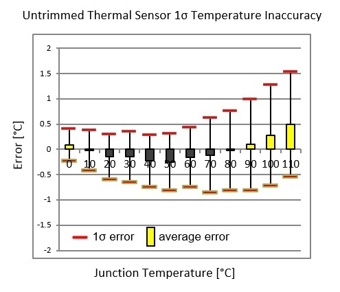
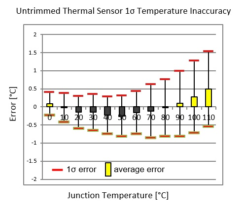
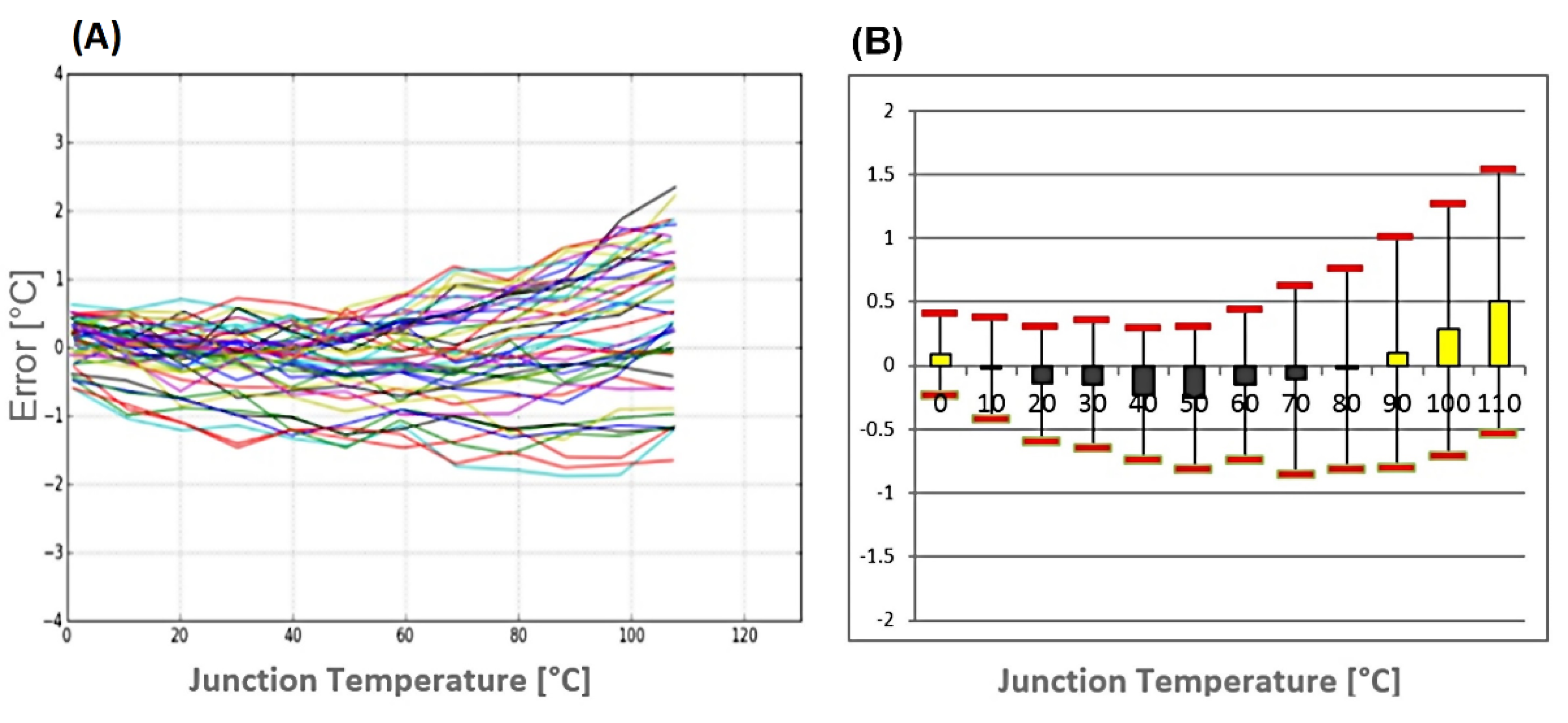
Finally, the untrimmed inaccuracy, without using any calibration, is quite low (
Figure 9) paving the way for using this TS without calibration for most SoC products. The error for 29 devices is ±2 °C in Ratiometric mode (
Figure 9A). The average temperature error is <0.5 °C and the resolution is ±0.25 °C without any averaging of reading samples. The one sigma error is less than 1 °C (
Figure 9B) and the three sigma error is less than ± 3 °C. Such inaccuracy is close to the results achieved by a practical calibration process such as using thermal diode. It means that calibration is unnecessary.
Figure 9.
Untrimmed inaccuracy of thermal sensors in Ratiometric mode. (A) Temperature error versus junction temperature without calibration for 29 devices; (B) Statistics of errors presented in A. The yellow rectangle indicates the average error in a specific temperature and the error bar indicates the standard deviation (1σ) of the error.
In
Table 2 you can see a comparison made with other TS available in the literature. The TS described in this article shows a very good performance in power, area and speed while maintaining good accuracy even without calibration.
Table 2.
Comparison with other TSs in the literature. Abs—absolute temperature error.
Table 2.
Comparison with other TSs in the literature. Abs—absolute temperature error.
| Reference | Sebastiano [3] | Souri [4] | Lakdawala [5] | Shor [2] | “High Sampling Rate” | “Power Saving Mode” |
|---|
| Source/Year | JSSC 2010 | JSSC 2013 | JSSC 2009 | JSSC 2013 | This work | This work |
| Technology | 65 nm | 0.16 μm | 32 nm | 22 nm | 22 nm | 22 nm |
| Area (mm2) | 0.1 | 0.08 | 0.02 | 0.0061 | 0.013 | 0.013 |
| Voltage Regulator | not required | not required | required | not required | not required | not required |
| Calibration | not required | not required | not required | required | not required | not required |
| Supply Voltage (V) | 1.2–1.3 | 1.5–2 | 1.05 | 1.35 | 1.25 | 1.25 |
| Current | 8.3 μA | 3.4 μA | 1.5 mA | 1.03 mA | 780 μA | 15–60 μA |
| Speed (samples/s) | 2.2 | 10–188 | 1 K | 2 K–20 K | 5 K–45 K | 10–100 |
| Energy/Sample (J) | 4.5 μ | 27 n–440 n | 1.6 μ | 69.5 n–0.69 μ | 30 n–270 n | 750 n–1.88 μ |
| Accuracy with/out calibration (°C) | 0.2/0.5 (3Σ) | 0.15[0.25]/0.6[0.8] (3Σ) | /5 (abs) | 1.5 (abs) | 1.8/2 (abs) | 1.8/2 (abs) |
| Range | −70 to 125 | −55 to 125 | −10 to 110 | −10 to 100 | −10 to 110 | −10 to 110 |
| Accuracy FOM (J%2) * | 47.3 n | 0.75 n | 27.7 μ | 679 n | 67.5 n | 1.6 μ |
7. Summary
In this paper we presented a precise low power integrated thermal sensor. The architecture uses advanced features such as dynamic element matching, precise regulated cascode current mirror, chopping, and correlated double sampling to overcome accuracy and matching issues. Silicon validation performed demonstrates immunity to process variation and an error <±1.8 °C for a range of 0–110 °C with a single temperature calibration.
Some of the configurability options were demonstrated, showing reference-based and Ratiometric operation. In the Ratiometric mode, a reference may not be needed as it is extracted by the ADC from the sense stage itself. Many additional configuration options, such as remote diode interfaces, signal path gain control, diode current ratio control and digital post processing options make this architecture a fertile testing ground for the exploration of temperature sensing techniques.
The untrimmed inaccuracy of the thermal sensor is less than ±3 °C (3σ) across the entire range. Reducing the calibration process will significantly reduce the tester cost for SoC products.
Over all, the silicon results show a unique ability to trade between high sampling rates and low power consumption up to 18 μW while retaining high accuracy without calibration in a small die area.


