Article

Interconnections between Electronic Structure and Optical Properties of Multilayer Nanolaminate TiAlN/Ag and Al2O3/Ag Coatings

1
Surface Phenomena Researches Group, I.P. Bardin Central Research Institute for Ferrous Metallurgy, 23/9 bdg. 2, Radio str., 105005 Moscow, Russia
2
Instituto de Ciencia de Materiales de Madrid, Consejo Superior de Investigaciones Científicas, E-28049 Madrid, Spain
3
Surface Engineering and Precision Institute, School of Aerospace, Transport and Manufacturing (SATM), Cranfield University, College Road, Cranfield, Bedfordshire MK43 0AL, UK
*
Author to whom correspondence should be addressed.
Coatings 2018, 8(8), 290; https://doi.org/10.3390/coatings8080290
Submission received: 27 April 2018 / Revised: 11 August 2018 / Accepted: 11 August 2018 / Published: 18 August 2018
(This article belongs to the Special Issue Surface Engineering and Nanofilms)

Abstract

:
Multilayer nanolaminate TiAlN/Ag and Al2O3/Ag metal-insulator-metal (MIM) coatings with thicknesses of individual layers from a few to several hundreds of nanometers were fabricated by direct current magnetron sputtering. Their optical transmittance and reflectance spectra were measured for photon energies 1–5 eV (1240–248 nm). The spectra were non-monotonous as their transmission and reflection bands were strongly dependent on the coating architecture. A set of advanced electron spectroscopy methods was used to analyse the electronic structure of the coatings controlling optical properties. Energies of plasmons peaks and the distribution of their intensities are functions of the Ag layers thickness as well as the composition and thickness of the dielectric nanolayers in the MIM nanocomposite. Statistical analysis established the cross-correlations between geometrical parameters of the coatings, transmissions and reflection bands on the optical spectra and parameters of the electronic structure. Particularly, the blue side of the transmittance band is controlled by plasmons while the dielectric band gap determines the transmittance of the red side. The obtained experimental results allowed us to fulfil the computed architectural design of a multilayer Al2O3/Ag coating with a narrow bandwidth in the visible light region and strong reflection in the infrared and ultraviolet regions.

1. Introduction

Thin-film multilayer metal-dielectric (MIM) coatings are a new class of plasmon metamaterials whose interaction with external electromagnetic radiation is caused by lattice-scattering effects. The characteristic dimensions are several orders lower than the wavelengths of the radiation. MIM nanocomposite materials are demonstrating properties sharply distinctive from the bulk phases. External electromagnetic radiation in these artificial materials excites plasmon and phonon waves that are transforming the initial radiation. Surface plasmon-polariton (SPP) interactions result from the coupling between collective oscillations of conducting electrons (plasmons) in metal and lattice waves (phonons) in dielectrics [1,2]. SPP modes with a high local density of optical states (DOS) could actively transform the intensity and spectral shape of the light reflecting from or transmitting through the nanolayer MIM coating. Excitation of plasmons at optical frequencies and their relaxation with photons emission are the processes allowing manipulation with spectral intensities of the transmitted and reflected light in metal-dielectric metamaterials with dimensions of structural elements one or two orders less than the electromagnetic wavelength. Sub-nanometer accuracy in MIM coatings architecture establishes conditions for the localisation and propagation of plasmon electromagnetic radiation, providing specific optical and thermal conductivity properties. The physical paradox is that the confinement in nanostructured materials opens new possibilities. Multiple interesting properties, such as invisible negative refraction and artificial magnetism, will provide a broader space for exploring novel optical devices based on plasmonic metamaterials [3], cloaking devices [4], superlenses [5], microelectromechanical systems (MEMS) [6], and solar cells [7,8], which are all candidate applications of metamaterials. Solar energy is a very promising field of application of thin-film planar MIMs. Antireflection coatings are widely used in solar cells, including third generation PV. The films aim to reduce and control the reflection from the surface of the panels. Multilayer thin film coating on the solar panel has the function of spectral control considering the spectral response characteristics of the absorbing layer of the solar cell in addition to the antireflective function. These planar MIM coatings have the prospect to reduce optical and electrical losses and improve conversion efficiency. Recent progress in nanotechnology provides the possibility to control the refractive index of some materials (i.e. the speed at which light propagates in material), and it could be highly beneficial for photovoltaic applications.
Solar photo-thermal conversion plants also need new solar selective coatings with high light absorbance in the wavelength range 0.3–2.5 μm and low thermal emittance in the infrared (IR) region (2.5–30 μm). For parabolic trough concentrated solar power applications, solar selective coating solutions based on paint coatings that work up to 400 °C are sufficient and employed regularly, but economic and environmental concerns push for further improvements in the efficiencies of modern renewable technologies. Central receiver concentrated solar power technologies require high absorbance and low emittance in combination with thermal stability in significantly more severe environments. Our previous research [9,10] has shown that nanolaminate multilayer coatings based on nitrides and noble metals have high wear resistance and anomalously low thermal conductivity.
As previously reported in [11], the surface reflectivity coefficient R depends on the reflective index n and the extinction coefficient k as:
R ( T e , T p , ω ) = ( n 1 ) 2 + k 2 ( n + 1 ) 2 + k 2
The reflective index n(ω) can be presented as a function of angular plasmon frequency ωp, total scattering rates νm, the angular frequency of the light ω, and extinction coefficient k as:
n 2 = 1 2 [ ( 1 ω p 2 ω 2 + ν m 2 ) + ( ν m ω ω p 2 ω 2 + ν m 2 ) 2 ] 1 2 + 1 2 ( 1 ω p 2 ω 2 + ν m 2 )
The bulk plasmon frequency of the material ωp,
ω p = N e · e 2 ε · m e f f
where Ne, ε, and meff are the density of conducting electrons, dielectric permittivity and the effective mass of the conduction electrons, respectively.
The influence of the ionic lattice on the conduction electrons can be accounted for using an effective mass of the electron meff instead of me. According to the Drude–Lorenz (DL) model, the refractive index depends on the plasmon frequency.
Therefore, we studied experimentally how nanostructuring influences frequencies and the spatial distribution of excited plasmons. Confinement of plasmon resonance and polariton coupling in such coatings ensure good optical properties in the visible light range. Most bright design ideas for creating MIM plasmon metamaterials based on theoretical calculations are still experimentally unconfirmed [12,13]. One key disadvantage of such calculations is that they are based on the physical parameters of bulk materials. The classical laws of electromagnetic radiation propagation are disturbed in nanostructured plasmon metamaterials due to sharp transformations of the electronic structure affected by quantum size effects. The inflected electronic structure alters the physical properties of materials [14,15]. For this reason, the development of new plasmon planar MIM coatings with a perfect thermal barrier and optical properties is a complex engineering problem requiring experimental investigations of the propagation of plasmon and phonon waves in thin-film MIM materials during their miniaturisation. Visualization of such subtle phenomena developing at atomic scales requires special techniques combining high-resolution microscopy, atomic, and electron spectroscopy. Currently, there is only a limited number of such unique studies [16,17,18].
The present research is dedicated to studies of the functions of metal and dielectric layer parameters in MIM planar metamaterials in the spatial localisation of plasmon excitations in connection with their optical properties in the wideband, from infrared (IR) to ultraviolet (UV). The key scientific problem is the establishment of interconnection between the structural localization of plasmon excitations and optical filtering properties of nanolaminate MIM coatings for the design of new prospective antireflection coatings.

2. Materials and Methods

2.1. Parameters of Multilayer Coatings

DC-magnetron sputtering was used to deposit a set of multilayer TiAlN/Ag and Al2O3/Ag coatings. Individual layers had thicknesses from one to several hundred nanometers, listed in Table 1. The samples had additional protective 200 nm nitride or oxide layers to avoid Ag oxidation. Single layer coatings were also deposited as references.
TiAlN and Al2O3 were selected as dielectrics with narrow and wide bandgaps, correspondingly. Silver nanolayers or nanoparticles are widely used in optical metamaterials design.
The layered structure of the coatings was verified by Rutherford backscattering spectrometry (RBS). The measurements were performed with the 5 MV Cockroft–Walton tandetron (HVEE B.V., Amersfoort, Netherlands) at the Centro de Microanálisis de Materiales (CMAM) in Madrid (Spain) using a 2 MeV He+ probing beam and the backscattered ions were detected with a silicon detector at a scattering angle of 170°. The experimental RBS spectra were compared with simulated ones obtained from the SIMNRA code [19] assuming the corresponding sample layer structure. It was evidenced that interfaces are well defined and do not have any intermixing.

2.2. Parameters of Electron Spectroscopy Experiments

Electron spectroscopy Experiments were performed on the multifunctional electron spectrometer ESCALAB MK2 (VG, East Grinstead, UK) equipped by a monochromatic Al Kα X-ray source (hν = 1486.6 eV), scanning electron gun LEG200, and EMU-50 source of monochromatic electrons (E0 = 1–100 eV). C 1s photoelectron peak (Eb = 285.0 eV) was used as an internal reference to precisely determine photoelectron line positions. The samples were sputter cleaned by Ar+ ions in the preparation chamber of the spectrometer at a pressure of 10−5 Pa, an accelerating voltage of 5 kV, and a current of 20 µA. The precise control over the lateral Ar+ ion etching profile attained with the AG-6 ion gun (VG, East Grinstead, UK) was used to fabricate 0.25° angle laps. Ion etching with simultaneous sample rotation was used for thinning of the Al2O3 layer from 200 to 10 nm, its subsequent removal, and for the uniform thinning of Ag layers. The parameters of spectra acquisition were selected to provide high energy spectral resolution with a full width at half maximum (FWHM) about 20 meV for high-resolution electron energy loss spectroscopy (HREELS, investigations using EMU-50 source. Scanning Auger electron microscopy (AEM) and scanning electron microscopy (SEM) of characteristic losses (LEG200 source) were used for mapping of the elements and plasmon intensities distribution through the cross-section of the multilayer coatings in individual layers and near the interfaces. Primary electron energies E0 were of 1371.4 and 1401.5 eV. Resolution of images was 256 × 256 pixels at 10,000× magnification. Image acquisition software was used to suppress the topographical contrast.

2.3. Modelling of Optical Properties

As published in [11], DL model and Transfer Matrix Method (TMM) were used to determine optical constants of MIMs fitting the experimental data for light reflection. Such fitting was based on the Levenberg–Marquardt algorithm, which provided the best solution search procedure.
According to the DL model, a complex dielectric function ε (ε1 and ε2 are the real and imaginary components of the dielectric function, correspondingly) of a material
ε(ω) = ε1(ω) + i·ε2(ω)
could be presented as:
ε = ε ω p 2 f j ω j 2 ω 2 + i ω G j , ω 0 = 0
where ωp is the bulk plasmon frequency, ω is the primary light frequency; ωj is j-th the resonant frequency of the system, Gj is a damping coefficient.
The complex refractive index N = n + i·k is an essential attribute of the planar MIM that describes absorption and reflection of the light interacting with these films.
Refraction (n) and extinction (k) coefficients were calculated as:
n = ε 1 2 + ε 2 2 + ε 1 2 ; k = ε 1 2 + ε 2 2 ε 1 2

3. Results and Discussion

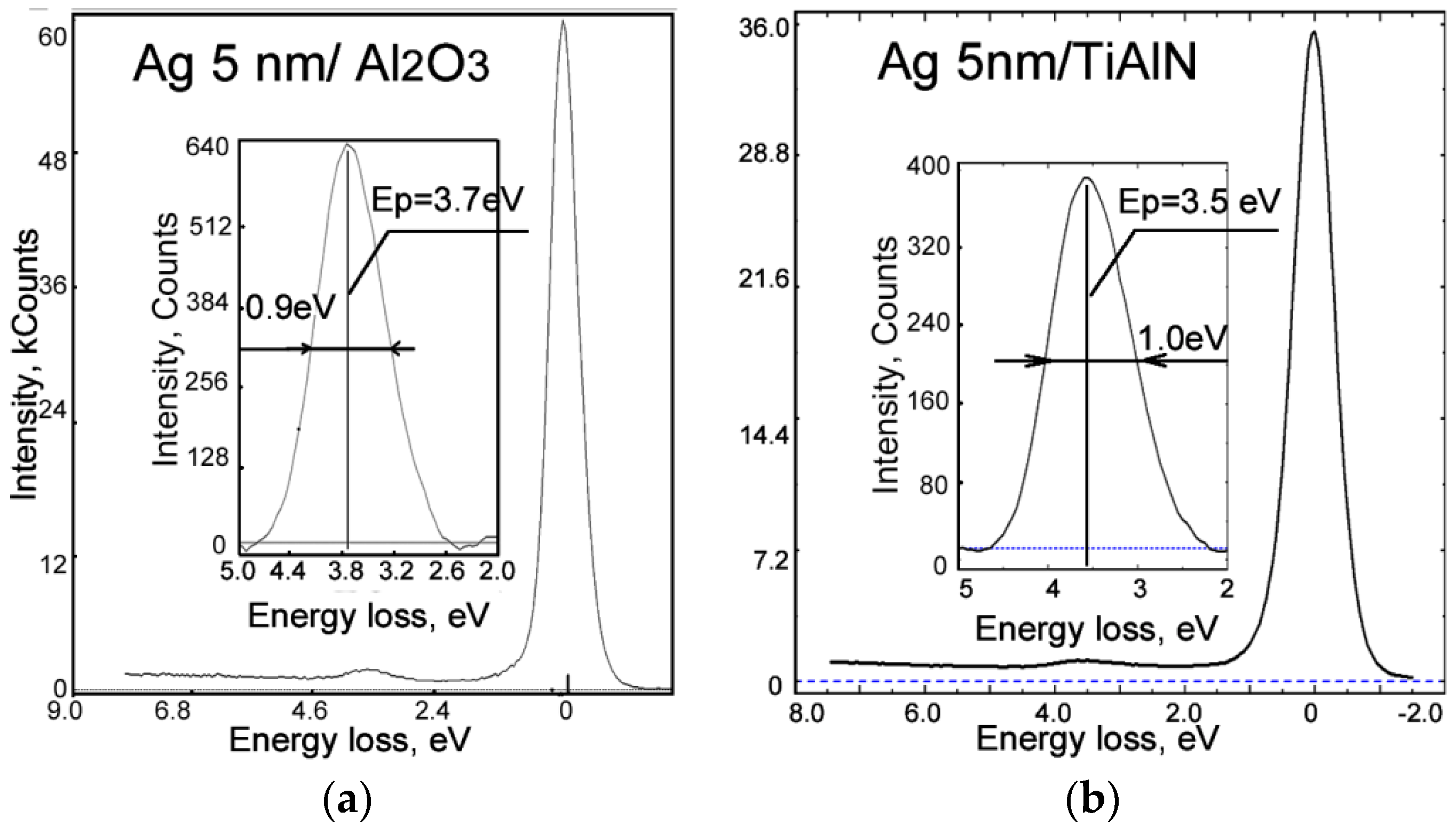
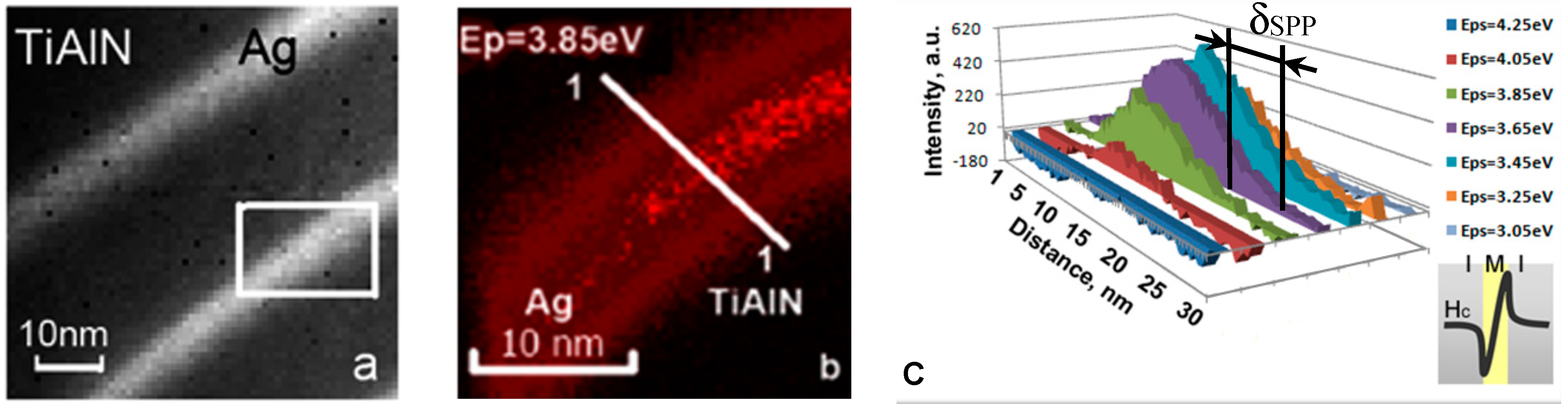
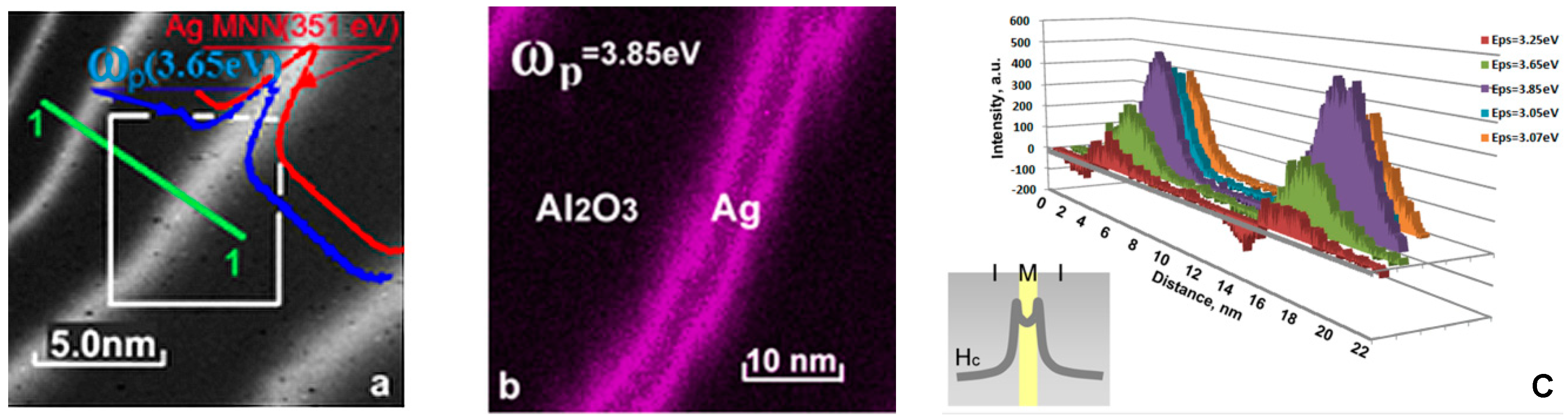
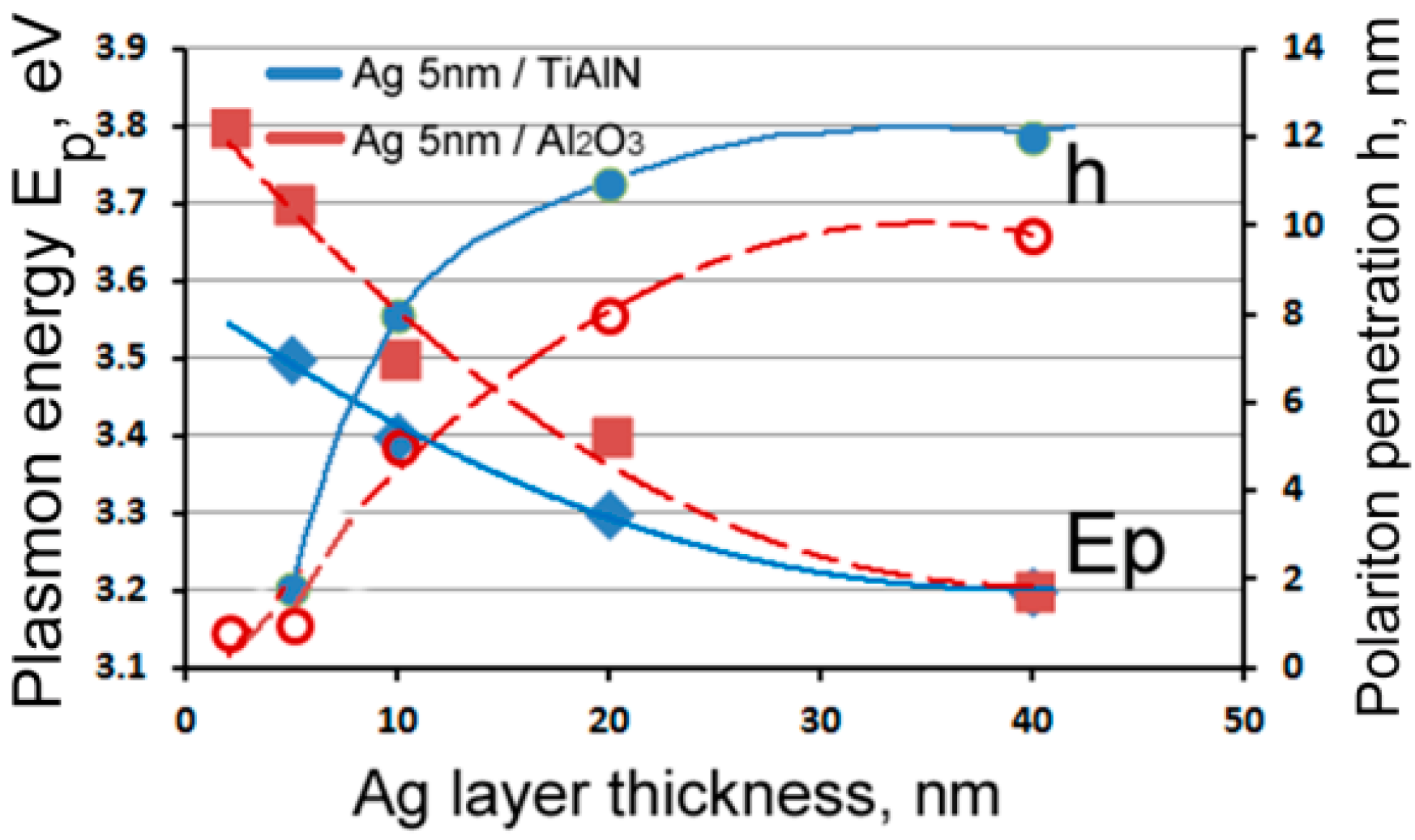
3.1. Experimental Studies of Plasmon Losses

Figure 1 demonstrates electron energy loss spectroscopy (EELS) acquired from 5 nm thick Ag layers in MIM multilayer coatings with Al2O3 (Figure 1a) and TiAlN (Figure 1b). Inserts on these figures depict magnified surface plasmon peaks. It is observed that peak energies and half-widths (FWHM) of plasmon losses lines are different for these coatings. The Ag layer thickness in these MIM planar composites was the same.
It is most likely that these features can be explained by the difference in dielectric surrounding of silver layers. Multiple processes of electron energy losses control the half-width of plasmon excitations line (FWHM). Particularly the plasmon-polariton interaction at the interface phase contributes significantly to the FWHM of the plasmon peak. The observed widening of energy losses lines means the growth of the plasmon lifetime and therefore its mean free path. The plasmon lifetime τ stipulated by its adsorption by an electron passing from one band to another was calculated firstly in [20]. It could be expressed easily through the optical constants n (reflectance index) and k (extinction coefficient) as:
1/τ = n·k·ω
The dependences of these parameters with Ag layer thickness for Ag/TiAlN coatings were presented in [18].
Microimages of angle laps of 10/20 Ag/TiAlN and 5/24 Ag/Al2O3 coatings and 2D distribution of plasmon excitation at a resonance frequency of 3.85 eV are shown in Figure 2 and Figure 3, correspondingly. These data were obtained by SEM and plasmon electron microscopy. The line distributions of plasmon (ωp) signals demonstrate the antisymmetrical (Figure 2c) or symmetrical (Figure 3c) distribution of surface plasmons in the cross-section of 10 and 5 nm Ag layers.
Inserts on Figure 2c and Figure 3c depict the magnitudes of the magnetic field (Hy). Excited Hy modes profile clearly show the antisymmetric or symmetric plasmon mode distribution. Plasmon contrasts for two different silver films correspond to the spatial distribution of the magnetic field Hy [21]. Figure 2b,c (Ag 10 nm) and Figure 3b,c (Ag 5nm) show that the antisymmetric plasmon resonance is excited in the thicker Ag nanolayer while the symmetric one excites in the thinner layer. Figure 2b,c (Ag 10 nm) and Figure 3b,c (Ag 5nm) show that the antisymmetric plasmon resonance is excited in the thicker Ag nanolayer while the symmetric one excites in the thinner layer.
For finite values of layer thickness, the electromagnetic interaction between the two interfaces cannot be neglected. The surface plasmon-polariton at one interface “senses” the existence of the other on the opposite interface, a “repulsion of levels” occurs. The dispersion curves for the surface plasmon-polariton are localised at each of the two interfaces are becoming distorted by the interaction of these waves [22]. This complex overlapping of plasmon strands along the interfaces produces the spatial inhomogeneity of plasmon excitation. The symmetric or antisymmetric shape of the plasmons spatial distribution depends on their energy [17]. The penetration depth of the SP field for thin silver film becomes smaller as it depends on the plasmon resonance energy. This interconnection is shown in Figure 4.
The transboundary penetration depth δSPP depends on the wavelength λ0, the energy of plasmon resonance [23] and properties of the metal and the dielectric as:
δ SPP = c E p ( ε m ) 2 2 π ( ε m ) ( ε m + ε d ε m ε d ) 3 2
where c is the light velocity in the metal, Ep is the plasmon resonance energy, ε m is a real part of the relative permittivity of the metal, ε m is an imaginary part of the relative permittivity of the metal, εd is a relative permittivity of the dielectric.
The dependences of Ep and δSPP on the thickness of Ag layers (Figure 4) are in full accordance with Equation (8).
The plasmon energies are more prominent in thinner nanolayers due to electronic structure transformations. Plasmons in thin layer of Ag with both s and d-bands crossing the Fermi level are typically strongly damped by the presence of interband transitions. According to [17], Ag 5s electrons DOS growth is a common reason for increasing plasmon energy with metal nanolayer thinning. The increased binding energy of the plasmon with ion core (localised 5s electrons) provides more intense excitation energy as we observed with a damping Ag layer thickness in the nanometer range. Such growth of the surface plasmon energy at nanostructuring was demonstrated in [24,25] for silver clusters. This definite shift of plasmon peak to higher frequency is also called “blue shift”. The dielectric environment of the silver layers has a significant effect on the depth of transboundary plasmon penetration from the metal into the dielectric and on the energy of plasmon resonance. The effect is partly due to the difference in the dielectric properties (εd) of Al2O3 and TiAlN. The permittivity of Al2O3 is three times higher in comparison with TiAlN [26,27]. These nanoscale features of plasmon resonance can directly influence the optical properties (reflection, transmission, absorption) of planar metamaterials.

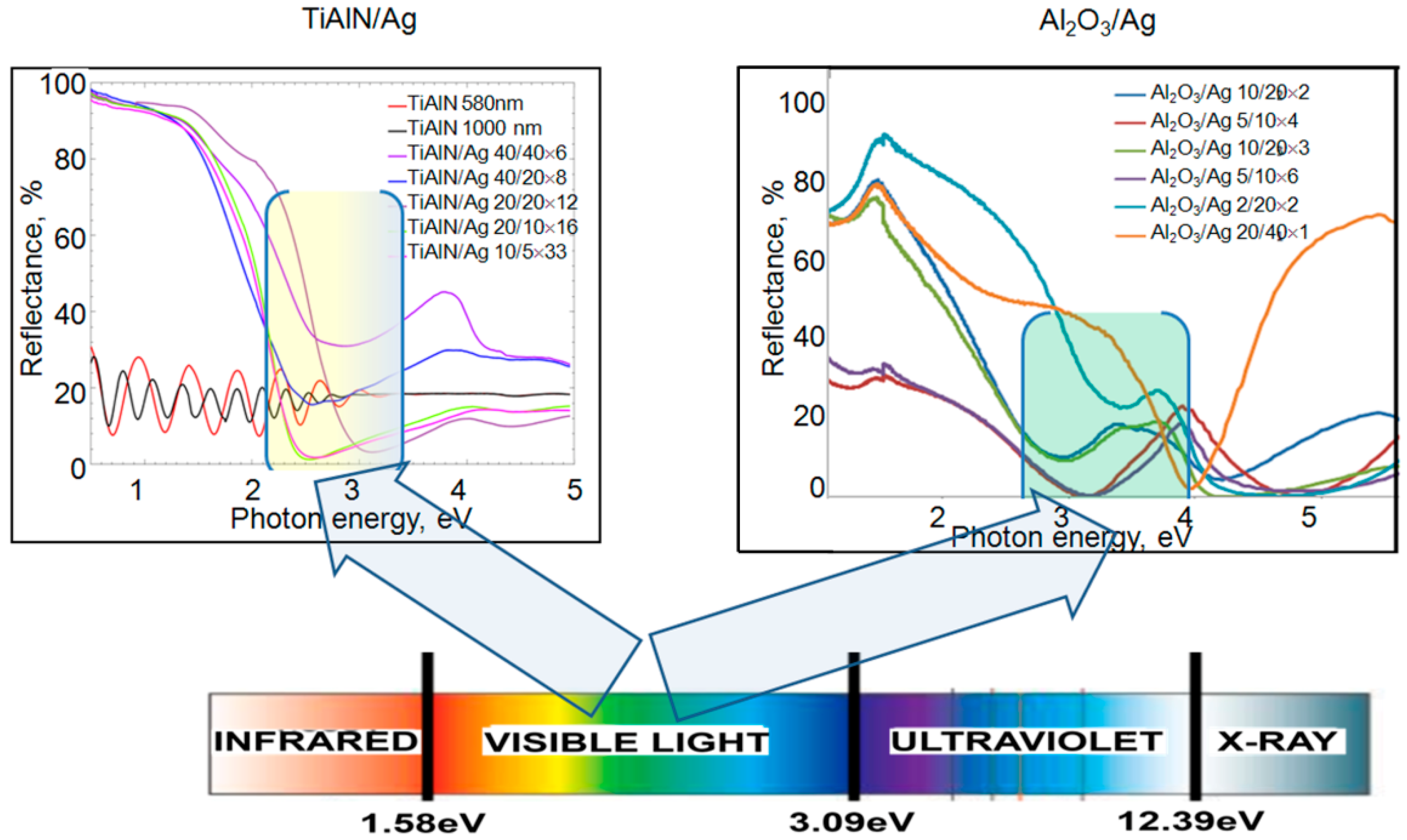
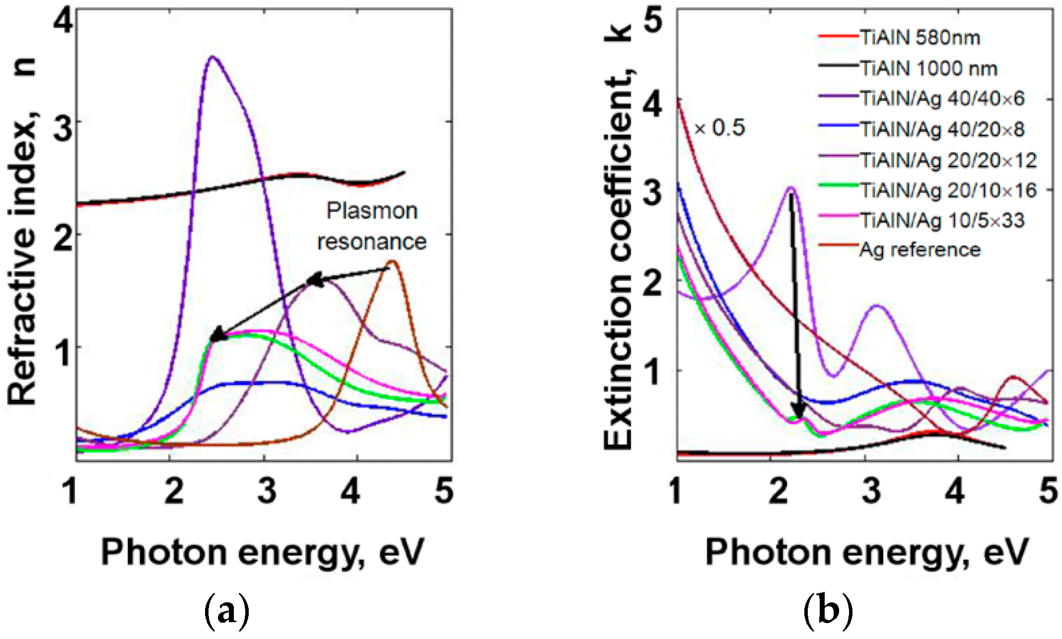
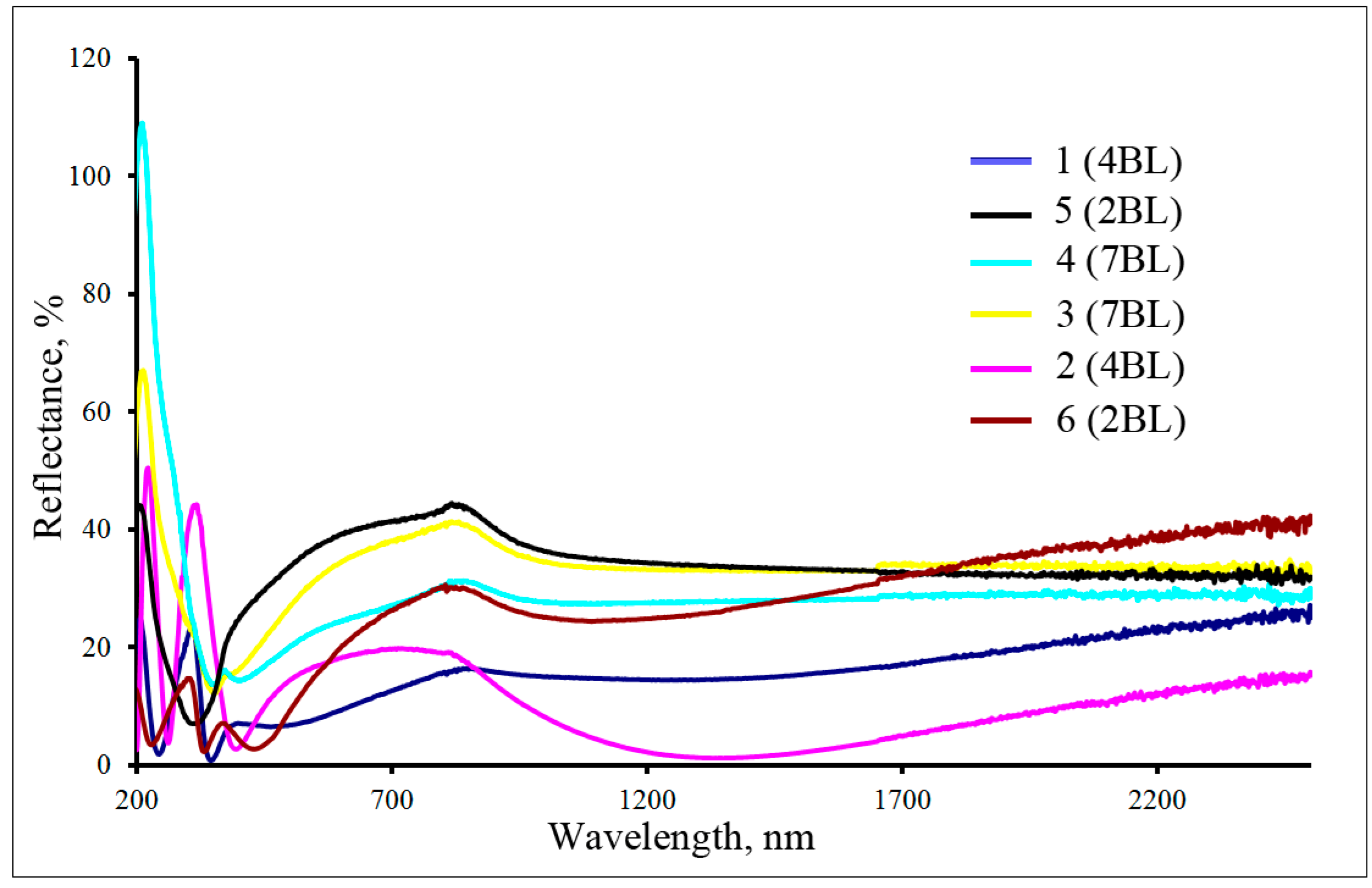
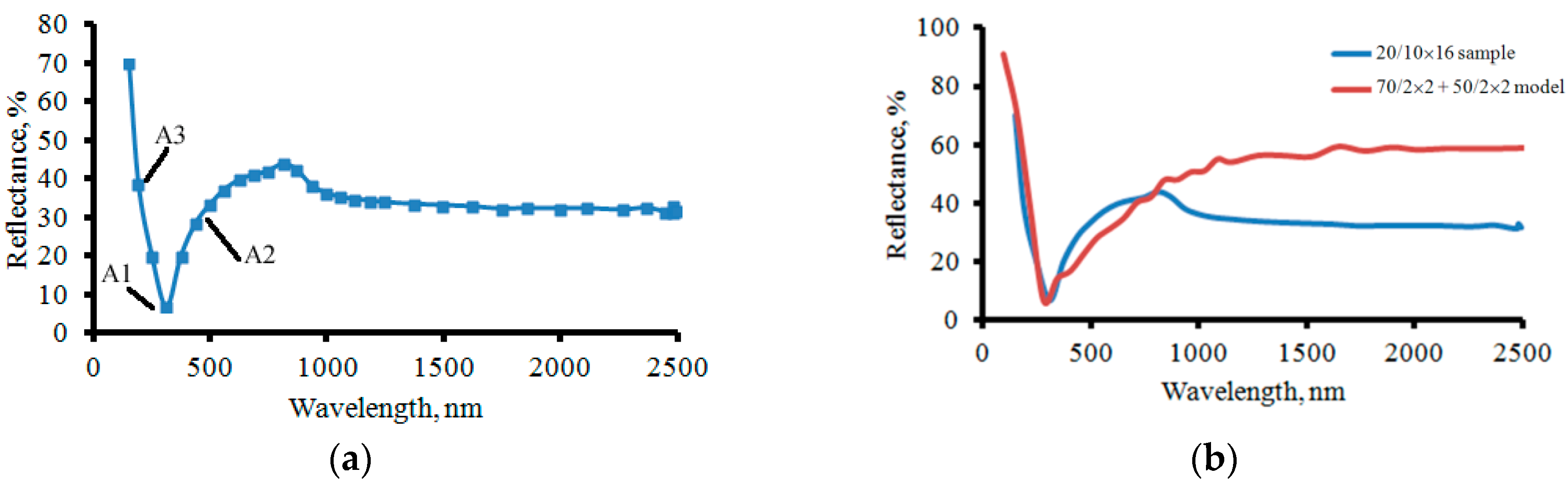
3.2. Features of Light Reflection Spectra

Reflection spectra for coatings with various layer thicknesses and a number of “metal-dielectric” bilayers are presented in Figure 5. One can see that each multilayer coating has its band of maximal reflection suppression near the frequency ω0 = λ0c corresponding to resonant adsorption by surface plasmon resonance. In the long waves region at ω < ω0 the reflectance is growing with ω decreasing, and the threshold of reflectance is shifted according to ω0 variation. The resonance frequency of adsorption is shifted to longer waves at a growing number of bilayers with the same thicknesses (Figure 5).
The maximal transmittance at long waves is attenuated with the growth of the bilayers number with a widening of the transmittance band for frequencies ω > ω0. Transmittance diapasons differ for TiAlN/Ag and Al2O3/Ag multilayer coatings. Figure 4 demonstrates that each Al2O3/Ag coating has a larger plasmon resonance energy than TiAlN/Ag with the same metal thickness. The transmittance band coincides with the energy of the plasmon resonance forming the “blue shift” of the transmittance in Al2O3/Ag coatings.
Similar interaction of plasmons with light in TiO2-coated Au nanoparticles was presented in [28].
Figure 6 demonstrates the complex influence of the Ag/TiAlN coatings architecture on their reflectance. So, the coating with 40 nm layers of Ag and TiAlN (ML-40/40 × 06) possesses a reflectance over 30% in the whole measured band of photon energies. Anti-reflectance properties of this coating are poor enough.
The reflectance level near ω0 is decreased significantly, and the transmittance bandwidth is expanded with by thinning the individual layers and increasing their number. We can see it clearly comparing reflectance curves for 40/40 × 06, 20/40 × 06 and 5/10 × 33 coatings, where the reflectance goes down to 30%, 15%, and 1.0%, correspondingly. Increasing of the layers number in the coatings with thin (≤10.0 nm) layers shifts the transmittance band to long waves with a smaller reflectance. Therefore the coating 5/10 × 33 adsorbs light with λ < 540 nm (2.3 eV) with an efficiency of more than 90%. This coating filters photons with λ > 540 nm. The key property of these coatings is an adsorption bandwidth with low reflection coefficients. Comparing the spectral data for the coatings with different layers thicknesses but approximately the same total thickness h (ML 20/20 × 12, h = 480 nm; ML 10/10 × 24, h = 480nm; and ML 05/10 × 33, h = 495 nm) we see that the adsorption band near ω0 is widening with Ag layers thinning. This regularity is also observed when comparing the width of the plasmon resonance zones in these coatings. One can see a growing plasmon peak FWHM from 0.6, 0.8 eV up to 1.0 eV with the Ag layer thinning in the row 40.0, 20.0, and 5.0 nm. Adsorption of the light in Ag/TiAlN planar nanocomposites results from the excitation of plasmon oscillation in the silver layers as well as plasmon-polariton interactions on the “metal-dielectric” interfaces. The energy (or resonance frequency) and width of the selective adsorption range of the electromagnetic radiation are correlating with the energy band of the plasmon resonance in the planar metamaterial. According to Equations (1) and (6), this correlation is a complex one.
We can control the reflection of the incident light in the red-IR spectral band and its adsorption with a very small reflection in the visible range through the architecture of the nanocomposites. The solar light spectrum has a high intensity in the photons energies range 2.0–3.0 eV. Thus, the control of coatings transmission and reflection properties is important for many applications including helioenergetics.
As it was shown in [11], the energy of the main plasmon peak in TiAlN/Ag coatings grows with Ag layers thinning. This is the well known “blue shift” in nanomaterials. The minimum light reflection also moves to shorter waves. It was also found also that frequencies of plasmons resonating with Ti 3d or Ag 5s electrons in TiAlN depend on the thicknesses of either insulator or metallic individual layers. Such kind of resonance gives two absorption edges (or Lorenz terms) with close resonant frequencies ωi but with significantly different attenuation times Gi. According to our calculations, both plasmon and polariton attenuation times (Figure 5b) are 4–5 times lower for 10/5 and 20/10 TiAlN/Ag coatings than for 40/40 one.
Al2O3/Ag coatings are demonstrating similar qualitative regularities, but alumina as a strong dielectric provides smaller depths of plasmons penetration. These coatings have a reflection minima at higher photon energies than TiAlN/Ag ones with the same thickness of Ag layers.
We can conclude that plasmons in metal layers of MIM coatings are controlled by the effective thickness of the metal layers that could be described as their geometrical thickness plus the plasmon penetration depth in the dielectric material.

3.3. Architectural Design of MIM Multilayer Coatings based on Ag/Al2O3

Prediction of the optimal MIM architecture, characterised by a deep and a narrow bandwidth in the visible light region and intensive reflection in the IR and UV ranges of electromagnetic radiation requires a numerical solution of several analytical problems. DL and TMM models allowed us to determine the optical constants for each group of silver and alumina bilayers. These characteristics were obtained for all the spectra shown in Figure 7.
For the next step, the position of characteristic points A1, A2, and A3 (Figure 8a) were determined for each spectrum for the characterisation of the best filtering properties of the material. These points were chosen at a minimum and half the heights for the boundaries of the transmission window.
The correlation analysis established the dependence of the position of these points on the number of bilayers, the thickness of the individual metal and dielectric layers, and other parameters of the MIM coating architecture (as shown in Table 2). The pairs of variables with positive Pearson correlation coefficients (p) values below 0.050 are tending to increase together. For the pair with negative correlation and p values below 0.050 in magnitude, one variable tends to decrease while the other increases. For pairs with p values greater than 0.050, there is no significant relationship between the two variables.
Pearson correlation reveals that the point A3 depends inversely on the plasmon-polariton interaction, A1 is directly proportional to the thickness of the coating, and A2 is directly proportional to the thickness and band gap of the dielectric.
The reflectance spectrum of the multilayer plasmon MIM metamaterial as a function of Ag and Al2O3 layer thickness and number of bilayers was synthesised. Previously calculated optical constants for a bilayer Ag/Al2O3 coating and correlation dependences were used to model the reflection spectra of the MIM films with different architecture. This process was repeated several times. We have found that approximately five iterations of geometry realisations are necessary to optimise the experimentally observed reflection spectra of the Ag/Al2O3 MIM coating. An example of the simulated and experimental spectra is shown in Figure 8b. We have calculated the reflection spectra of the complex multilayer MIM coating using a mathematical model and compared it with experimental results.
The transmittance properties in the visible light band of the simulated spectrum (brown line) are in strong agreement with the experimental result (blue line) and have better reflective properties in other areas of the spectrum.

4. Conclusions

In this study, optical transmission and reflection properties of MIM nanolaminates containing high- and low-k dielectric layers were measured. Comprehensive electron spectroscopy studies including scanning plasmon microscopy were performed to reveal the physical mechanisms responsible for non-monotonous reflection and transmission of light. Interconnections between metal layer thickness and the maximum plasmon resonance position, the half-width of plasmon peak and the width of the light absorption band were determined. For the first time, the fine characteristics of plasmon excitation and transboundary propagation in MIM nanostructures were studied experimentally by direct methods of electron spectroscopy. Plasmon electron microscopy with a unique spatial resolution was realized for the study of plasmon confinement. These studies overcome the limitations of computer modeling for the studying of plasmonic metamaterials. The following conclusions are drawn based on the experimental work:
  • Surface plasmon-polariton interactions on “metal-dielectric” interfaces are increasing the effective thickness of metal nanolayers.
  • IR and UV cut-off positions are shifted through the electromagnetic spectrum depending on the plasmonic system parameters, namely thickness and the number of layers in the system.
  • Ag/TiAlN and Ag/Al2O3 nanocomposite systems could be used as broadband optical coatings with high light transmission and low reflection at a selected wavelength range of electromagnetic spectrum with nearly total IR reflection and relatively high (60%) reflection of UV. The total thickness of such coatings could be one or two orders smaller than a light wavelength.
  • Their transmittance and reflectance bands could be tuned by the selection of individual layers thicknesses for a metal and a dielectric, the number of bilayers, as well as by the selection of the dielectric. These light filtering coatings could be fabricated using different metals and dielectrics.

Author Contributions

Conceptualization, A.K., D.W. and J.E; Investigation, D.W., A.K., V.V., R.G.; Formal Analysis, V.V.; Visualization, D.W., A.K., V.V.; Writing-Original Draft Preparation, D.W., A.K.; Writing-Review & Editing, D.W., A.K., V.V., R.G., J.E.

Funding

The research was partially supported by RSF research project No. 14-12-00170.

Conflicts of Interest

The authors declare no conflict of interest.

Nomenclature

AbbrevationExpansion
MIMmetal-insulator-metal
SPsurface plasmon
SPPsurface plasmon-polariton
DOSdensity of states
MEMSmicroelectromechanical system(s)
IRinfrared
UVultraviolet
DLDrude–Lorenz
DCdirect current
FWHMfull width at half maximum (half-width)
HREELShigh-resolution electron energy loss spectroscopy
EELSelectrons energy losses spectroscopy
REELSreflection electrons energy losses spectroscopy
SEMscanning electron microscopy
AEM(scanning) Auger electron microscopy
TMMTransfer Matrix Method
VariableMeaningDimension
Rsurface reflectivity coefficient
nreflective index
kextinction coefficient
ωangular frequency1/s
ωpangular frequency of the plasmon1/s
νmscattering rate1/s
Nedensity of conducting electrons1/m3
εdielectric permittivity
memass of the electronkg
meffeffective mass of the conduction electronskg
E0primary energyeV
Hymagnitude of the magnetic fieldA/m
ΔEenergy losseseV
δSPPtransboundary penetration depth of the plasmonm
clight velocitym/s
Epplasmon resonance energyeV
ε m real part of the relative permittivity of a metal
ε m imaginary part of the relative permittivity of the metal
εdrelative permittivity of the dielectric
λwavelengthm

References

  1. Maier, S.A. Plasmonics: Fundamentals and Applications; Springer: Berlin, Germany, 2007. [Google Scholar]
  2. Boriskina, S.V.; Tong, J.K.; Huang, Y.; Zhou, J.; Chiloyan, V.; Chen, G. Enhancement and tunability of near-field radiative heat transfer mediated by surface plasmon polaritons in thin plasmonic films. In Photonics; Multidisciplinary Digital Publishing Institute: Basel, Switzerland, 2015; Volume 2, pp. 659–683. [Google Scholar]
  3. Li, M.; Huang, L. Perspective on resonances of metamaterials. Opt. Express 2015, 23, 19022–19033. [Google Scholar] [CrossRef]
  4. Cai, W.; Chettiar, U.K.; Kildishev, A.V.; Shalaev, V.M. Optical cloaking with metamaterials. Nat. Photonics 2007, 1, 224–227. [Google Scholar] [CrossRef] [Green Version]
  5. Kim, M.; Rho, J. Metamaterials and imaging. Nano Converg. 2015, 2, 22. [Google Scholar] [CrossRef] [PubMed]
  6. Kanamori, Y.; Hokari, R.; Hane, K. MEMS for plasmon control of optical metamaterials. IEEE J. Sel. Top. Quantum Electron. 2015, 21, 137–146. [Google Scholar] [CrossRef]
  7. Wang, Y.; Sun, T.; Paudel, T.; Zhang, Y.; Ren, Z.F.; Kempa, K. Metamaterial-plasmonic absorber structure for high efficiency amorphous silicon solar cells. Nano Lett. 2012, 12, 440–445. [Google Scholar] [CrossRef] [PubMed]
  8. Green, M.A.; Pillai, S. Harnessing plasmonics for solar cells. Nat. Photonics 2012, 6, 130–132. [Google Scholar] [CrossRef]
  9. Kovalev, A.I.; Wainstein, D.L.; Vakhrushev, V.O.; Gago, R.; Soldera, F.; Endrino, J.L.; Fox-Rabinovich, G.S.; Veldhuis, S. Features of electronic and lattice mechanisms of transboundary heat transfer in multilayer nanolaminate TiAlN/Ag coatings. Sci. Rep. 2017, 7, 17078. [Google Scholar] [CrossRef] [PubMed] [Green Version]
  10. Kovalev, A.I.; Wainstein, D.L.; Rashkovskiy, A.Y.; Gago, R.; Soldera, F.; Endrino, J.L. The confinement of phonon propagation in TiAlN/Ag multilayer coatings with anomalously low heat conductivity. Appl. Phys. Lett. 2016, 108, 223106. [Google Scholar] [CrossRef]
  11. Wainstein, D.L.; Vakhrushev, V.O.; Kovalev, A.I. Control of optical properties of metal-dielectric planar plasmonic nanostructures by adjusting their architecture in the case of TiAlN/Ag system. J. Phys. Conf. Ser. 2017, 857, 012054. [Google Scholar] [CrossRef] [Green Version]
  12. Yang, H.; Li, J.; Xiao, G. Significantly increased surface plasmon polariton mode excitation using a multilayer insulation structure in a metal–insulator–metal plasmonic waveguide. Appl. Opt. 2014, 53, 3642–3646. [Google Scholar] [CrossRef] [PubMed]
  13. Babicheva, V.E.; Malureanu, R.; Lavrinenko, A.V. Plasmonic finitethickness metal-semiconductor-metal waveguide as ultracompact modulator. Photonic Nanostruct. Fundam. Appl. 2013, 11, 323–334. [Google Scholar] [CrossRef]
  14. Mosquera, A.; Horvat, D.; Rashkovskiy, A.; Kovalev, A.; Miska, P.; Wainstein, D.; Allbella, J.; Endrino, J.L. Exciton and core-level electron confinement effects in transparent ZnO thin films. Sci. Rep. 2013, 3, 1714. [Google Scholar] [CrossRef]
  15. Wainstein, D.L.; Kovalev, A.I. Regularities of electronic structure transformations in nanomaterials with decreasing their characteristic size. J. Phys. Conf. Ser. 2017, 857, 012055. [Google Scholar] [CrossRef] [Green Version]
  16. Bosman, M.; Ye, E.; Tan, S.F.; Nijhuis, C.A.; Yang, J.K.W.; Marty, R. Surface plasmon damping quantified with an electron nanoprobe. Sci. Rep. 2013, 3, 1312. [Google Scholar] [CrossRef] [PubMed]
  17. Kovalev, A.I.; Wainstein, D.L.; Rashkovskiy, A.Y.; Gago, R.; Soldera, F.; Endrino, J.L.; Fox-Rabinovich, G.S. Interface-induced plasmon nonhomogeneity in nanostructured metal-dielectric planar metamaterial. J. Nanomater. 2015, 16, 110. [Google Scholar] [CrossRef]
  18. Kovalev, A.I.; Rashkovskiy, A.Y.; Wainstein, D.L.; Gago, R.; Soldera, F.; Endrino, J.L. Influence of electronic structure, plasmon-phonon and plasmon-polariton excitations on anomalously low heat conductivity in TiAlN/Ag nanoscale multilayer coatings. Curr. Appl. Phys. 2016, 16, 459–468. [Google Scholar] [CrossRef]
  19. Mayer, M. SIMNRA User’s Guide 6.05; Max-Planck-Institut für Plasmaphysik: Garching, Germany, 2009. [Google Scholar]
  20. Wolff, P. Theory of plasma waves in metals. Phys. Rev. 1953, 92, 18–23. [Google Scholar] [CrossRef]
  21. Lee, W.-J.; Kim, J.-E.; Park, H.Y.; Lee, M.-H. Silver superlens using antisymmetric surface plasmon modes. Opt. Express 2010, 18, 5459–5465. [Google Scholar] [CrossRef] [PubMed]
  22. Zayats, A.V.; Smolyaninov, I.I.; Maradudin, A.A. Nano-optics of surface plasmon polaritons. Phys. Rep. 2005, 408, 131–314. [Google Scholar] [CrossRef]
  23. Barnes, W.L. Surface plasmon–polariton length scales: A route to sub-wavelength optics. J. Opt. A Pure Appl. Opt. 2006, 8, S87–S93. [Google Scholar] [CrossRef]
  24. Ealet, B.; Elyakhloufi, M.H.; Gillet, E.; Ricci, M. Electronic and crystallographic structure of γ-alumina thin films. Thin Solid Films 1994, 250, 92–100. [Google Scholar] [CrossRef]
  25. Tiggesbiumker, J.; Koeller, L.; Meiweis-Broer, K.H.; Liebsch, A. Blue shift of the Mie plasma frequency in Ag clusters and particles. Phys. Rev. A 1993, 48, R1749. [Google Scholar] [CrossRef]
  26. Naik, G.V.; Schroeder, J.L.; Ni, X.; Kildishev, A.V.; Sands, T.D.; Boltasseva, A. Titanium nitride as a plasmonic material for visible and near-infrared wavelengths. Opt. Mater. Express 2012, 2, 478–489. [Google Scholar] [CrossRef]
  27. Robertson, J. High dielectric constant oxides. Eur. Phys. J. Appl. Phys. 2004, 28, 265–291. [Google Scholar] [CrossRef] [Green Version]
  28. Wang, X.; Sridhar, V.; Guo, S.; Talebi, N.; Miguel-López, A.; Hahn, K.; van Aken, P.A.; Sánchez, S. Fuel-free nanocap-like motors actuated under visible light. Adv. Funct. Mater. 2018, 28, 1705862. [Google Scholar] [CrossRef]
Figure 1. Electron energy loss spectroscopy (EELS) of Ag layers in 5 nm Ag/20 nm Al2O3 (a) and 5 nm Ag/24 nm TiAlN (b) multilayer coatings.
Coatings 08 00290 g001
Figure 2. Back scattered image of angle lap of 10/20 Ag/TiAlN coating (a); plasmon losses mapping (ΔE = 3.85 eV) (b); distribution of plasmon intensities across line 1-1 in dependence on plasmon energy ωp (c), δSPP—depth of plasmon-polariton transboundary penetration.
Coatings 08 00290 g002
Figure 3. Back scattered image of angle lap of 5/24 Ag/Al2O3 coating (a); plasmon losses mapping (ΔE = 3.85 eV) (b); distribution of plasmon intensities across line 1-1 in dependence on plasmon energy ωp (c).
Coatings 08 00290 g003
Figure 4. Energies of plasmon HREELS peaks Ep and depths of plasmon-polariton penetration at the metal/dielectric boundary δSPP vs Ag nanolayers thickness.
Coatings 08 00290 g004
Figure 5. Reflection spectra of multilayer TiAlN/Ag and Al2O3/Ag nanocomposites with various architectures given on inserts.
Coatings 08 00290 g005
Figure 6. Refractive index n (a) and extinction coefficient k (b) of deposited TiAlN/Ag coatings and Ag reference calculated using the Transfer Matrix Method (TMM).
Coatings 08 00290 g006
Figure 7. Reflection spectra of multilayer Al2O3/Ag nanocomposites with various architectures (see the legend and Al2O3 part in Table 1).
Coatings 08 00290 g007
Figure 8. The choice of characteristic points on sample 5 (2 BL) reflection spectrum (a); the comparison of the experimental (blue line) and optimised reflection spectrum (brown line) after computer modelling (b).
Coatings 08 00290 g008
Table 1. Composition parameters of multilayer coatings.
DielectricSample No.Dielectric Layer Thickness, nmAg Layer Thickness, nmNo. of Dielectric/Ag BilayersTotal Thickness, nm
Al2O31 (4 BL)4054180
2 (4 BL)4024168
3 (7 BL)2047168
4 (7 BL)81763
5 (2 BL)242252
6 (2 BL)245258
Al2O3 ref20001200
TiAlN1 (6 BL)40406480
2 (3 BL)1501503900
3 (33 BL)20533825
4 (16 BL)201016480
5 (6 BL)1502061020
6 (8 BL)30308480
7(33 BL)10533495
TiAlN ref.90001900
Table 2. Correlation of reflection spectra vs. characteristics of plasmon resonance and architecture parameters of MIM multilayer Al2O3/Ag coatings.
Point A2, nmPoint A3, nmMin. Reflection, %Al2O3 Layer, nm (Band Gap)Ag Layer, nm (ωp)Bilayer Thickness, nmTotal Thickness, nm (Attenuation Time τ)Number of Bilayers
Point A1, nm0.03590.1810.1360.0333−0.7660.09980.08920.0126
Point A2, nm0.7660.2330.01390.2530.3060.5420.442
Point A3, nm0.8520.34−0.01260.05470.4020.0023
Min. reflection, %0.5270.1570.1570.02030.783

