
Distinguishing Local Demagnetization Contribution to the Magnetization Process in Multisegmented Nanowires

 , , , , , , and
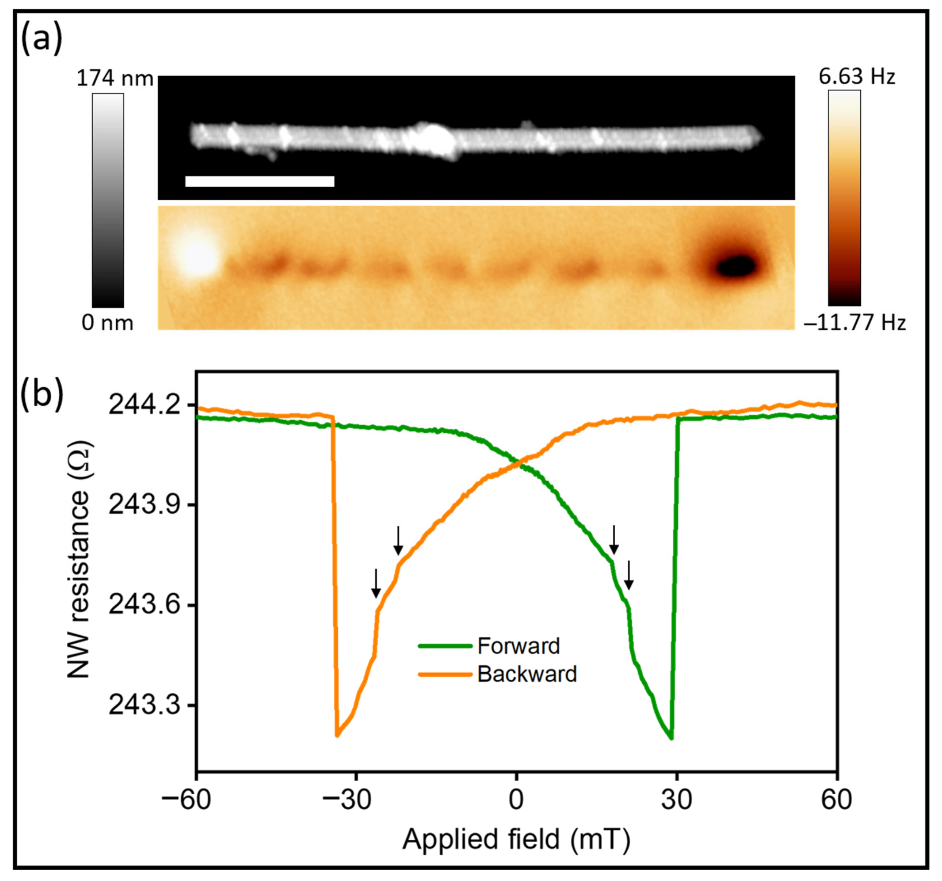
Abstract
:1. Introduction
2. Materials and Methods
3. Results and Discussion
3.1. Multilayered Nanowires
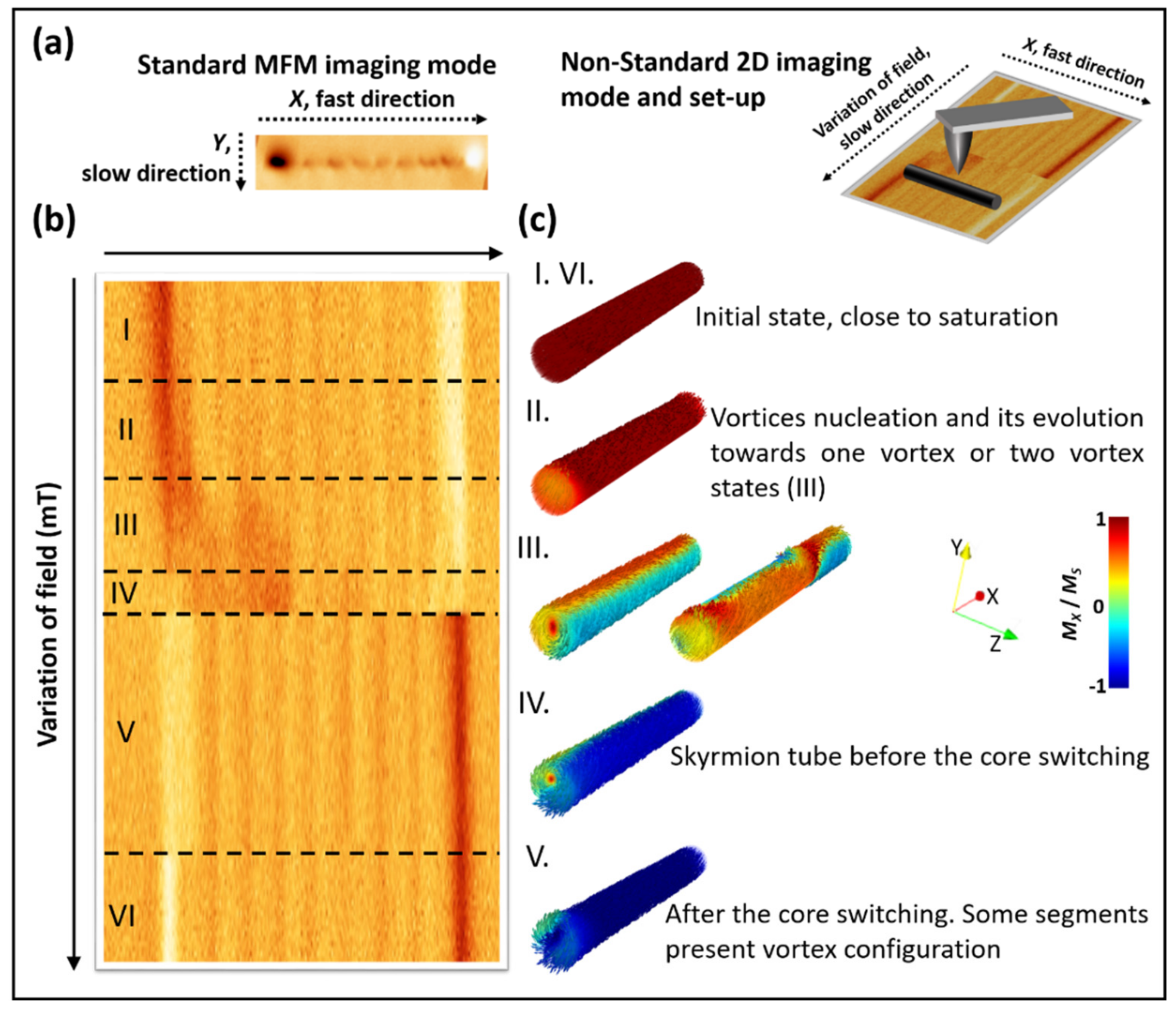
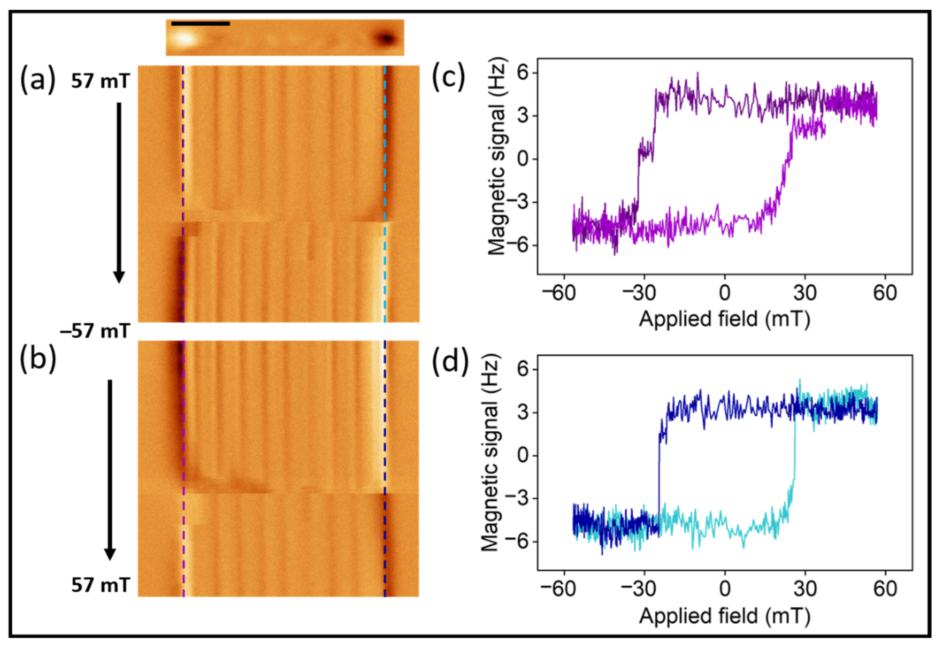
3.2. Magnetization Reversal Process Imaging by Advanced MFM
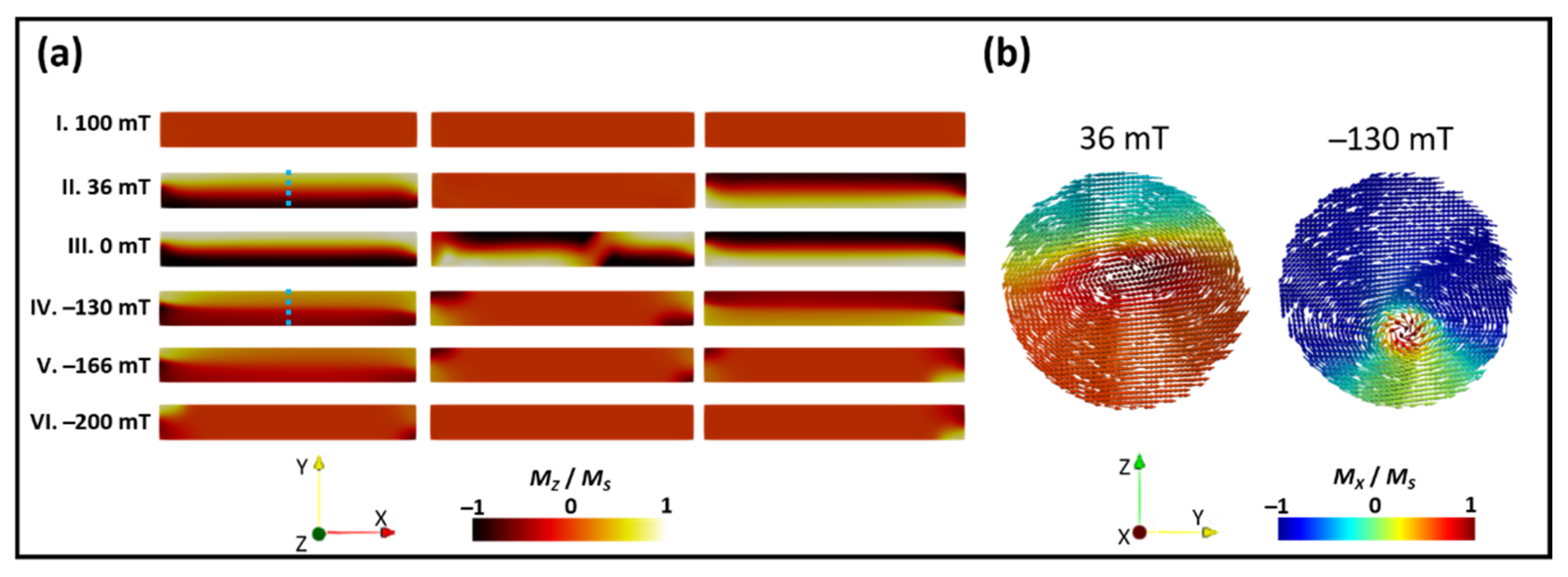
3.3. Micromagnetic Modelling
4. Conclusions
Supplementary Materials
Author Contributions
Funding
Institutional Review Board Statement
Informed Consent Statement
Data Availability Statement
Conflicts of Interest
References
- Streubel, R.; Fischer, P.; Kronast, F.; Kravchuk, V.P.; Sheka, D.D.; Gaididei, Y.; Schmidt, O.G.; Makarov, D. Magnetism in Curved Geometries. J. Phys. D Appl. Phys. 2016, 49, 363001. [Google Scholar] [CrossRef]
- Moreno, J.A.; Bran, C.; Vazquez, M.; Kosel, J. Cylindrical Magnetic Nanowires Applications. IEEE Trans. Magn. 2021, 57, 800317. [Google Scholar] [CrossRef]
- Ivanov, Y.P.; Alfadhel, A.; Alnassar, M.; Perez, J.E.; Vazquez, M.; Chuvilin, A.; Kosel, J. Tunable Magnetic Nanowires for Biomedical and Harsh Environment Applications. Sci. Rep. 2016, 6, 24189. [Google Scholar] [CrossRef] [Green Version]
- Özkale, B.; Shamsudhin, N.; Chatzipirpiridis, G.; Hoop, M.; Gramm, F.; Chen, X.; Martí, X.; Sort, J.; Pellicer, E.; Pané, S. Multisegmented FeCo/Cu Nanowires: Electrosynthesis, Characterization, and Magnetic Control of Biomolecule Desorption. ACS Appl. Mater. Interfaces 2015, 7, 7389–7396. [Google Scholar] [CrossRef] [PubMed] [Green Version]
- Mourachkine, A.; Yazyev, O.V.; Ducati, C.; Ansermet, J.P. Template Nanowires for Spintronics Applications: Nanomagnet Microwave Resonators Functioning in Zero Applied Magnetic Field. Nano Lett. 2008, 8, 3683–3687. [Google Scholar] [CrossRef]
- Bran, C.; Saugar, E.; Fernandez-Roldan, J.A.; del Real, R.P.; Asenjo, A.; Aballe, L.; Foerster, M.; Fraile Rodríguez, A.; Palmero, E.M.; Vazquez, M. Stochastic vs. Deterministic Magnetic Coding in Designed Cylindrical Nanowires for 3D Magnetic Networks. Nanoscale 2021, 13, 12587–12593. [Google Scholar] [CrossRef]
- Burks, E.C.; Gilbert, D.A.; Murray, P.D.; Flores, C.; Felter, T.E.; Charnvanichborikarn, S.; Kucheyev, S.O.; Colvin, J.D.; Yin, G.; Liu, K. 3D Nanomagnetism in Low Density Interconnected Nanowire Networks. Nano Lett. 2021, 21, 716–722. [Google Scholar] [CrossRef]
- Dawidek, R.W.; Hayward, T.H.; Vidamour, I.T.; Broomhall, T.J.; Venkat, G.; Mamoori, M.A.; Mullen, A.; Kyle, S.J.; Fry, P.W.; Steinke, N.-J.; et al. Dynamically-driven emergence in a nanomagnetic system. Adv. Funct. Mater. 2021, 31, 2008389. [Google Scholar] [CrossRef]
- Bran, C.; Berganza, E.; Fernandez-Roldan, J.A.; Palmero, E.M.; Meier, J.; Calle, E.; Jaafar, M.; Foerster, M.; Aballe, L.; Fraile Rodriguez, A.; et al. Magnetization Ratchet in Cylindrical Nanowires. ACS Nano 2018, 12, 5932–5939. [Google Scholar] [CrossRef]
- Berganza, E.; Jaafar, M.; Bran, C.; Fernández-Roldán, J.A.; Chubykalo-Fesenko, O.; Vázquez, M.; Asenjo, A. Multisegmented Nanowires: A Step towards the Control of the Domain Wall Configuration. Sci. Rep. 2017, 7, 11576. [Google Scholar] [CrossRef] [PubMed] [Green Version]
- Susano, M.; Proença, M.P.; Moraes, S.; Sousa, C.T.; Araújo, J.P. Tuning the magnetic properties of multisegmented Ni/Cu electrodeposited nanowires with controllable Ni lengths. Nanotechnology 2016, 27, 335301. [Google Scholar] [CrossRef] [PubMed]
- Berganza, E.; Bran, C.; Jaafar, M.; Vazquez, M.; Asenjo, A. Domain Wall Pinning in FeCoCu Bamboo-like Nanowires. Sci. Rep. 2016, 6, 29702. [Google Scholar] [CrossRef] [PubMed]
- Salem, M.S.; Sergelius, P.; Corona, R.M.; Escrig, J.; Görlitz, D.; Nielsch, K. Magnetic properties of cylindrical diameter modulated Ni80Fe20 nanowires: Interaction and coercive fields. Nanoscale 2013, 9, 3941–3947. [Google Scholar] [CrossRef] [PubMed]
- Bran, C.; Fernandez-Roldan, J.A.; del Real, R.P.; Asenjo, A.; Chubykalo-Fesenko, O.; Vazquez, M. Magnetic Configurations in Modulated Cylindrical Nanowires. Nanomaterials 2021, 11, 600. [Google Scholar] [CrossRef]
- Mohammed, H.; Moreno, J.A.; Kosel, J. Advanced Fabrication and Characterization of Magnetic Nanowires. In Magnetism and Magnetic Materials; Panwar, N., Ed.; InTech Open: London, UK, 2018. [Google Scholar]
- Reza Zamani Kouhpanji, M.; Stadler, B.J.H. Unlocking the Decoding of Unknown Magnetic Nanobarcode Signatures. Nanoscale Adv. 2021, 3, 584–592. [Google Scholar] [CrossRef]
- Rial, J.; Proenca, M.P. A Novel Design of a 3d Racetrack Memory Based on Functional Segments in Cylindrical Nanowire Arrays. Nanomaterials 2020, 10, 2403. [Google Scholar] [CrossRef]
- Bran, C.; Vázquez, M.; Berganza, E.; Jaafar, M.; Snoeck, E.; Asenjo, A. Magnetic Imaging of Individual Modulated Cylindrical Nanowires. In Magnetic Nano- and Microwires: Design, Synthesis, Properties and Applications; Vázquez, M., Ed.; Woodhead Publishing: Sawston, UK, 2020. [Google Scholar]
- Kazakova, O.; Puttock, R.; Barton, C.; Corte-León, H.; Jaafar, M.; Neu, V.; Asenjo, A. Frontiers of Magnetic Force Microscopy. J. Appl. Phys. 2019, 125, 060901. [Google Scholar] [CrossRef]
- Lau, J.W.; Shaw, J.M. Magnetic Nanostructures for Advanced Technologies: Fabrication, Metrology and Challenges. J. Phys. D: Appl. Phys. 2003, 44, 303001. [Google Scholar] [CrossRef]
- Rodríguez, L.A.; Magén, C.; Snoeck, E.; Serrano-Ramón, L.; Gatel, C.; Córdoba, R.; Martínez-Vecino, E.; Torres, L.; de Teresa, J.M.; Ibarra, M.R. Optimized Cobalt Nanowires for Domain Wall Manipulation Imaged by in Situ Lorentz Microscopy. Appl. Phys. Lett. 2013, 102, 0224178. [Google Scholar] [CrossRef] [Green Version]
- Wolf, D.; Rodriguez, L.A.; Béché, A.; Beécheé, B.; Javon, E.; Serrano, L.; Magen, C.; Gatel, C.; Lubk, A.; Lichte, H.; et al. 3D Magnetic Induction Maps of Nanoscale Materials Revealed by Electron Holographic Tomography. Chem. Mater. 2015, 27, 6771–6778. [Google Scholar] [CrossRef]
- da Col, S.; Jamet, S.; Rougemaille, N.; Locatelli, A.; Mentes, T.O.; Burgos, B.S.; Afid, R.; Darques, M.; Cagnon, L.; Toussaint, J.C.; et al. Observation of Bloch-Point Domain Walls in Cylindrical Magnetic Nanowires. Phys. Rev. B 2014, 89, 180405. [Google Scholar] [CrossRef] [Green Version]
- Rheem, Y.; Yoo, B.Y.; Beyermann, W.P.; Myung, N.V. Magnetotransport Studies of a Single Nickel Nanowire. Nanotechnology 2007, 18, 015202. [Google Scholar] [CrossRef]
- Kawamura, G.; Muto, H.; Matsuda, A. Hard Template Synthesis of Metal Nanowires. Front. Chem. 2014, 2, 104. [Google Scholar] [CrossRef] [PubMed] [Green Version]
- Lee, W.; Park, S.J. Porous Anodic Aluminum Oxide: Anodization and Templated Synthesis of Functional Nanostructures. Chem. Rev. 2014, 114, 7487–7556. [Google Scholar] [CrossRef] [PubMed]
- Fert, A.; Piraux, L. Magnetic Nanowires. J. Magn. Magn. Mater. 1999, 200, 338–358. [Google Scholar] [CrossRef]
- Vega, V.; Böhnert, T.; Martens, S.; Waleczek, M.; Montero-Moreno, J.M.; Görlitz, D.; Prida, V.M.; Nielsch, K. Tuning the Magnetic Anisotropy of CoNi Nanowires: Comparison between Single Nanowires and Nanowire Arrays in Hard-Anodic Aluminum Oxide Membranes. Nanotechnology 2012, 23, 465709. [Google Scholar] [CrossRef]
- Horcas, I.; Fernández, R.; Gómez-Rodríguez, J.M.; Colchero, J.; Gómez-Herrero, J.; Baro, A.M. WSXM: A Software for Scanning Probe Microscopy and a Tool for Nanotechnology. Rev. Sci. Instrum. 2007, 78, 013705. [Google Scholar] [CrossRef]
- Jaafar, M.; Serrano-Ramón, L.; Iglesias-Freire, O.; Fernández-Pacheco, A.; Ibarra, M.R.; de Teresa, J.M.; Asenjo, A. Hysteresis Loops of Individual Co Nanostripes Measured by Magnetic Force Microscopy. Nanoscale Res. Lett. 2011, 6, 407. [Google Scholar] [CrossRef] [Green Version]
- Mohammed, H.; Corte-León, H.; Ivanov, Y.P.; Moreno, J.A.; Kazakova, O.; Kosel, J. Angular Magnetoresistance of Nanowires with Alternating Cobalt and Nickel Segments. IEEE Trans. Magn. 2017, 53, 6001005. [Google Scholar] [CrossRef] [Green Version]
- Vansteenkiste, A.; Leliaert, J.; Dvornik, M.; Helsen, M.; Garcia-Sanchez, F.; van Waeyenberge, B. The Design and Verification of MuMax3. AIP Adv. 2014, 4, 107133. [Google Scholar] [CrossRef] [Green Version]
- Fernandez-Roldan, J.A.; Ivanov, Y.P.; Chubykalo-Fesenko, O. Micromagnetic Modeling of Magnetic Domain Walls and Domains in Cylindrical Nanowires. In Magnetic Nano- and Microwires: Design, Synthesis, Properties and Applications; Vázquez, M., Ed.; Woodhead Publishing: Sawston, UK, 2020. [Google Scholar]
- Berganza, E.; Marqués-Marchán, J.; Bran, C.; Vazquez, M.; Asenjo, A.; Jaafar, M. Evidence of Skyrmion-Tube Mediated Magnetization Reversal in Modulated Nanowires. Materials 2021, 14, 5671. [Google Scholar] [CrossRef] [PubMed]


Publisher’s Note: MDPI stays neutral with regard to jurisdictional claims in published maps and institutional affiliations. |
© 2022 by the authors. Licensee MDPI, Basel, Switzerland. This article is an open access article distributed under the terms and conditions of the Creative Commons Attribution (CC BY) license (https://creativecommons.org/licenses/by/4.0/).
Share and Cite
Marqués-Marchán, J.; Fernandez-Roldan, J.A.; Bran, C.; Puttock, R.; Barton, C.; Moreno, J.A.; Kosel, J.; Vazquez, M.; Kazakova, O.; Chubykalo-Fesenko, O.; et al. Distinguishing Local Demagnetization Contribution to the Magnetization Process in Multisegmented Nanowires. Nanomaterials 2022, 12, 1968. https://doi.org/10.3390/nano12121968
Marqués-Marchán J, Fernandez-Roldan JA, Bran C, Puttock R, Barton C, Moreno JA, Kosel J, Vazquez M, Kazakova O, Chubykalo-Fesenko O, et al. Distinguishing Local Demagnetization Contribution to the Magnetization Process in Multisegmented Nanowires. Nanomaterials. 2022; 12(12):1968. https://doi.org/10.3390/nano12121968
Chicago/Turabian StyleMarqués-Marchán, Jorge, Jose Angel Fernandez-Roldan, Cristina Bran, Robert Puttock, Craig Barton, Julián A. Moreno, Jürgen Kosel, Manuel Vazquez, Olga Kazakova, Oksana Chubykalo-Fesenko, and et al. 2022. "Distinguishing Local Demagnetization Contribution to the Magnetization Process in Multisegmented Nanowires" Nanomaterials 12, no. 12: 1968. https://doi.org/10.3390/nano12121968