1. Introduction
Nanowires (NWs) with quantum dots (QDs) have been intensively studied due to their potential applications, especially as a source of quantum light [
1,
2,
3]. In particular, it was shown that GaAs QDs in AlGaAs NWs are effective sources of single photons in the wavelength range 770–800 nm [
4,
5]. An important property of NW is its possibility to control spontaneous emission rates, providing an inhibition as well as an enhancement of spontaneous emissions (SE) [
6,
7,
8]. Tunneling of the spontaneous emissions of QD in NW into a single photonic mode is a critically important task for the realization of practical devices and many efforts have been made to provide directional emission of radiation from NW with QD [
9,
10,
11]. The common approach is based on an emission of QD into the fundamental waveguide mode HE
11, and a subsequent beaming of radiation via tapering of the shape of NW [
12,
13].
A concentration of the attention on the HE
11 mode (possessing non-zero radial component of the electric field near axis of the NW) is justified by the fact in GaAs quantum wells, and an electric dipole moment of the exciton ground state is oriented along the interface of quantum wells in the radial direction [
7,
10,
14,
15,
16].
The ideal approach to the fabrication of nanowires is the “bottom-up” approach [
1], in this case the grown nanowires are naturally aligned along the axis, which allows the emitter to interact in the best way with the modes of the waveguide. Authors of work [
17] present a quantum-dot-in-nanowire system that reproducibly self-assembles in core–shell GaAs/AlGaAs nanowires. In this case, it is extremely difficult to control the size and location of quantum dots. In turn, using the technology of sequential growth of NWs and QDs, it is possible to control the number and position of perfectly aligned emitters coupled with the same optical mode. This provides an excellent platform for studying and applying nanowires.
However, in the case of NWs with QDs, due to technological features, it is not always possible to grow NWs with a diameter suitable for the efficient confinement of the fundamental waveguide mode HE
11 (in the case of AlGaAs NWs with GaAs QDs, the NW diameter should be more than 180 nm [
6]). At the same time, some experimental and theoretical results indicate that coupling of light and heavy holes and light hole excitons, structural peculiarities and strains could lead to the appearance of pronounced axial component of an electric dipole in NW [
18,
19,
20,
21,
22,
23]. Therefore, it seems timely to expand investigation of SE in NW beyond fundamental HE
11 mode and analyze emission into TM
0 mode as well, which has a non-zero axial component of electric field and unlike HE
11 do not demonstrate suppression of SE for NW of small diameter.
In this paper, we present the results of experimental studies of directional radiation from GaAs QDs in AlGaAs NWs, where the NWs diameter is 130 nm (
Figure 1), and the theoretical results describing the probability of spontaneous QD emissions for various directions. For such thin NW couplings of emissions, the fundamental waveguided mode HE
11 is strongly suppressed [
5].
2. Materials and Methods
Growth experiments were carried out using molecular-beam epitaxy (MBE) setup Riber Compact 21T (Riber, Bezons, France) equipped, in addition to a growth chamber, with a chamber for Au deposition (metallization chamber). Polished Si (111) wafers were used as substrates. The growth was carried out in several stages. The surface of wafers was treated in a 10:1 aqueous solution of HF, and then the samples were loaded to the metallization chamber and heated up to the temperature of 850 °C for 10 min. After that, the sample temperature was decreased to 550 °C, and gold film of ~0.2 nm thickness was deposited in the metallization chamber. To allow for the formation of Au droplets on the surface, the substrate temperature was maintained for one minute, and then the samples were cooled down to the room temperature and was transferred to the growth chamber without breaking the ultrahigh vacuum conditions. In the growth chamber, the substrate temperature was increased to 510 °C, and the Al, Ga and As shutters were opened after temperature stabilization for AlGaAs NWs growth under As-stabilized conditions. The reflection of high-energy electron diffraction (RHEED) patterns indicated the formation of a pure wurtzite crystallographic phase of NWs after 2 min of growth, which did not change during the entire process. A typical RHEED pattern after 5 min growth of AlGaAs NWs is shown in
Figure S1. After 20 min of NW growth, GaA QDs were formed on top of the NWs by controllably closing the Al shutter for 15 s. Furthermore, the Al shutter was again opened for 45 s to form a cap layer. The QD formation procedure was repeated 10 times. At the final stage, the Al source shutter was opened for 5 min to form a cover layer. The nominal content of Al in the solid solution was set at 0.3 according to previous calibrations using a GaAs (100) substrate. The nominal growth rate of AlGaAs was kept constant at 1 monolayer per second (ML/s) during the whole experiment.
Morphological and structural properties of the grown samples were studied using a scanning electron microscope (SEM Supra 25, Carl Zeiss, Oberkochen, Germany) and a transmission electron microscope (TEM, JEOL 2100, JEOL Ltd., Tokyo, Japan) equipped with energy-dispersive X-ray spectroscopy analysis (EDX, X-Max 80, Oxford Ins., High Wycombe, UK). Optical properties of single NWs were examined using a micro-photoluminescence (μPL) setup (Princeton instruments, Trenton, NJ, USA) by a continuous-wave neodymium laser (wavelength 532 nm). A silicon-charged-coupled device (CCD) (Princeton instruments, Trenton, NJ, USA) was used as a photodetector. PL measurements were taken at a temperature of 4K in a closed cycle helium cryostat (Cryovac, Troisdorf, Germany). An optical microscope (Attocube, Haar, Germany) installed inside the cryostat allowed in situ control of the sample surface in the laser excitation region. Additionally, the setup is allowed to document macroPL from the array of NWs with QDs using a defocused laser beam. A typical spectrum from the array of AlGaAs NWs with GaAs QDs is shown in
Figure S2.
3. Results
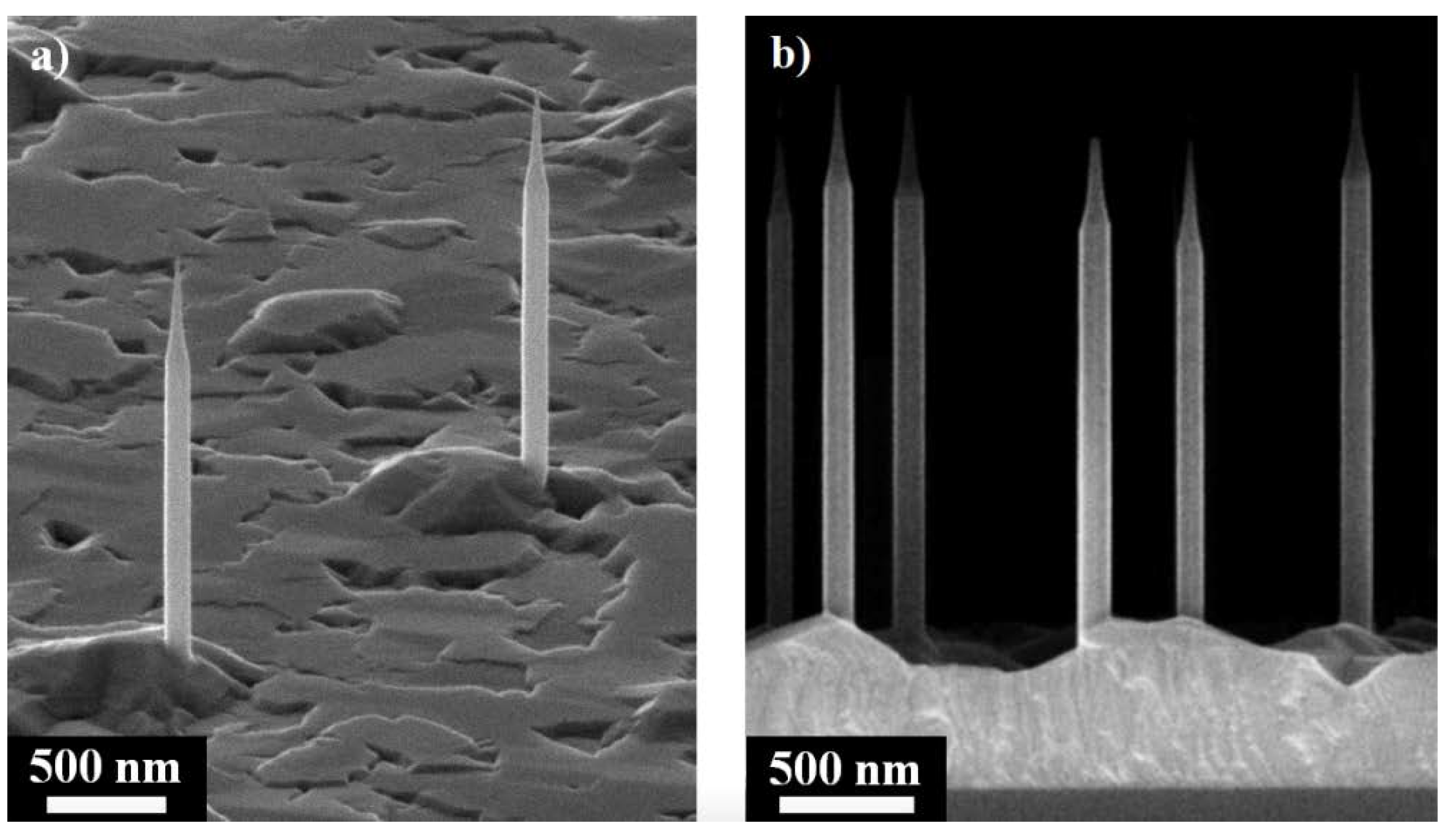
Typical SEM images of grown AlGaA NWs with GaAs QDs are shown in
Figure 1a,b. It is seen that AlGaAs NWs have a pencil-like shape, with a diameter of 130 nm at the bottom and 20 nm at the top of NWs. The AlGaAs NWs formed 2 μm length strongly in the <111> direction, which indicates their epitaxial bond with the Si substrate (111). It is important to note that the surface density of NWs, corresponding to the density of gold droplets on the substrate surface, turned out to be 3 × 10
7 cm
−2. Such a density made it possible to excite a single NW on some areas of the substrate. In addition, a quasi-two-dimensional AlGaAs layer between the NWs on the surface of the substrate was observed.
According to our previous works, under the described growth conditions, AlGaA NWs are spontaneously formed by a core-shell structure [
24]. Moreover, in the case of nominal Al
0.3Ga
0.7A composition, the real content of aluminum in the AlGaAs NW core is 16%, and 24% in the shell [
25].
The GaAs QDs diameter is equal to the diameter of the AlGaAs NWs core [
4], which, in turn, is determined by the size of the Au catalyst droplet, ~30 nm in our case [
24]. Accordingly, in our case, the thickness of the NWs shell is ~50 nm. Knowing the growth time and height of the NWs, we can determine the heights of the GaAs QDs and the AlGaAs barrier between QDs, which are ~10.5 nm and ~45 nm, respectively. Examination by the EDX technique of the grown NWs confirmed the estimated values of both QDs and barriers (
Figure S3).
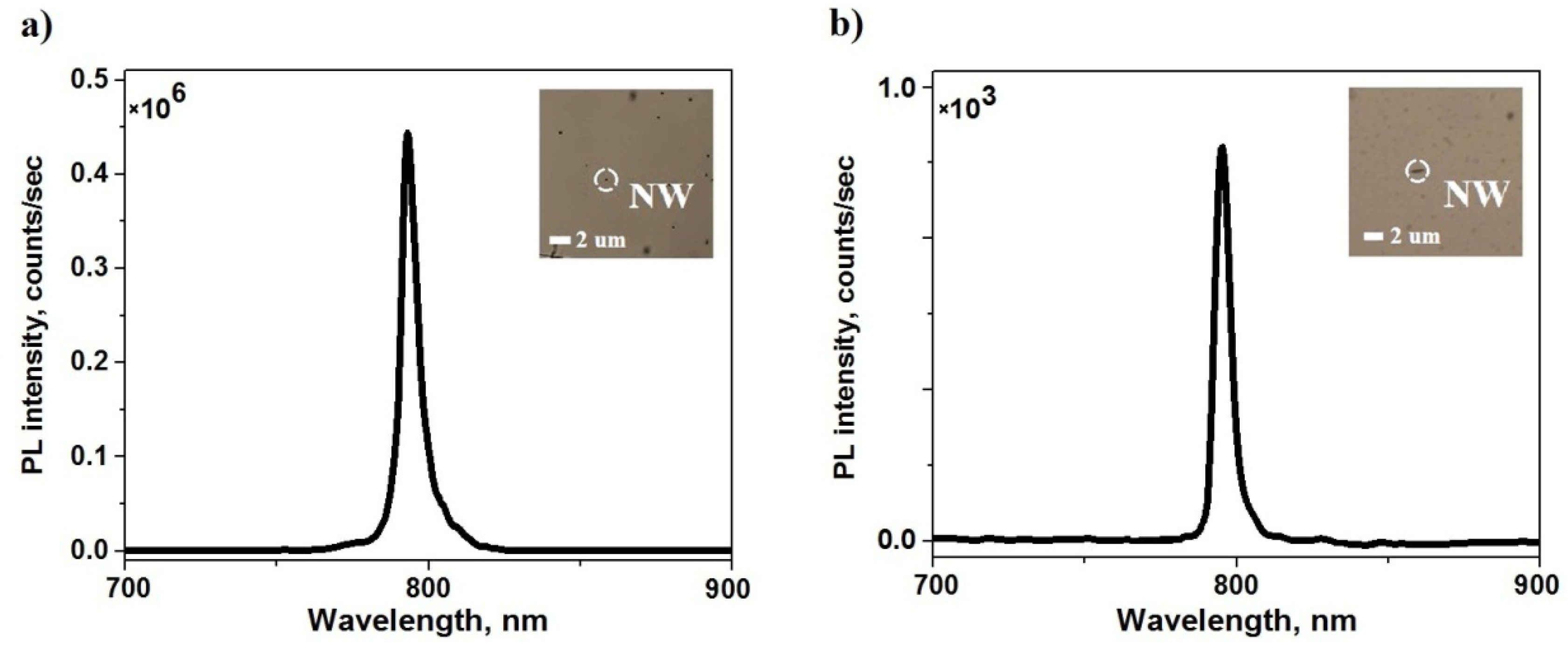
To compare the intensity of emission from QDs in different directions, part of the NW was removed from the substrate surface and placed on the surface of a clean silicon wafer.
Figure 2 shows typical μPL spectra under identical conditions, corresponding to emission from GaAs QDs in single AlGaAs NWs grown in a direction perpendicular to the surface of the Si substrate (
Figure 2a), as well as those dispersed onto the Si surface single NW (
Figure 2b). In both cases, the PL signal from the QDs was collected in the direction perpendicular to the substrate surface.
The insertions in
Figure 2a,b show the images of single standing and lying on the Si surface NW made with an optical microscope during the detection of μPL spectra. As can be seen from the figures, the wavelengths of the μPL spectra peaks are almost identical in both cases and amount to ~795 nm. However, the μPL intensity of lying on the surface nanostructure is ~2 orders of magnitude lower than that of not removed from the substrate surface. It is important to note that in the absence of the NWs within the laser beam, the μPL signal was not observed. This fact excludes the influence of the quasi-two-dimensional layer formed during the synthesis of NWs on the obtained μPL spectra. All of the above indicates that the μPL emission from GaAs QDs in AlGaAs NWs follows the direction of the NW growth. In
Figure S4 we present PL spectra taken from different standing and lying NWs showing the same trend.
4. Theory
There are only two types of cylindrical waveguide modes with a non-zero electric field at the NW axis: TM-polarized modes with the azimuthal number m = 0 and HE/EH modes with m = ±1. TM modes have an electric field parallel to the NW axis (axial filed direction), whereas modes with m = ±1, which include the fundamental HE
11 mode, demonstrate an electric field perpendicular to the structure axis (radial field direction). The leaky modes responsible for direct radiation into outer space have the same electric field direction on the axis (see
Supplementary Information (Section S2)). In the local response approximation, the quantum dots in the center of NW will radiate only into the aforementioned modes. The intensity of spontaneous emission into these modes is proportional to the square amplitude of axial (for TM modes) or radial (for |m| = 1 modes) components of the dipole matrix element of the ground optical transition in quantum dots under study.
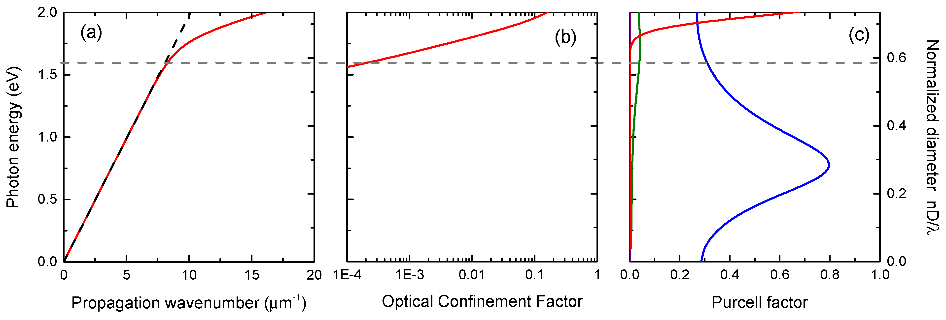
Figure 3a demonstrates the dispersion dependence for the HE
11 mode in NW with a diameter 130 nm. It can be seen that formally the waveguided mode exists for any photon energy, but below 1.5 eV it coincides with the light cone for the air (media outside NW). In
Figure 3b, a calculation of the optical confinement factor g of the HE
11 mode is presented, which is defined as a relation of the electromagnetic field energy inside NW to the total energy in the mode. One may see that in the low energy/diameter region where the HE
11 dispersion curve approaches the light cone, factor g plunges to extremely small values. This means that despite formal existence of the waveguided mode HE
11 in that region, the electromagnetic field is delocalized and the interaction of a quantum dot inside NW with the fundamental HE
11 mode is weak. For the photon energy 1.55 eV corresponding to the emission of QD (shown by horizontal dashed line in
Figure 3), the optical confinement factor g is about 8 × 10
−5.
It is convenient to describe the modification of emission efficiency by Purcell factors defined as spontaneous emission rates into particular channels divided by an emission rate of a QD in homogenous bulk material. Purcell factors for spontaneous emission of a radial-dipole optical transition into HE
11 mode (red curve) and into leaky modes (green curve) are shown in
Figure 3c alongside a total Purcell factor for axial-dipole transition (blue curve), which in the considered range of photon energies or diameters coincides with the Purcell factor for TM-polarized leaky modes (see
Supplementary Information (Section S2)). It can be seen that for the diameter of NW 130 nm and photon energy 1.55 eV emission into waveguided mode HE
11 is suppressed: the value of the Purcell factor is about 5.6 × 10
−5. On the other hand, for the leaky modes interacting with a radial–dipole transition in the QD Purcell factor has the value 3.7 × 10
−2, which exceeds the corresponding value for the waveguided mode HE
11 by three orders of magnitude.
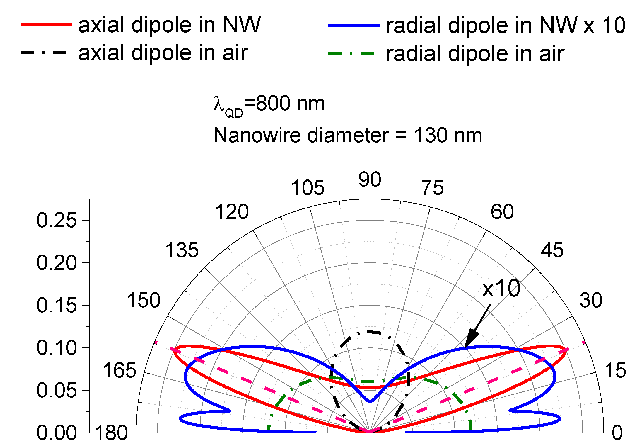
It interesting to analyze how NW modifies the directionality of the emitted radiation. The blue line in
Figure 4 shows the directionality diagram for a radial–dipole optical transition (in this case an emitter placed on the NW axis radiates through HE/EH leaky modes with c azimuthal number |m| = 1). It can be seen that radiation is confined within the cone around the NW axis with the angle at approximately 45 degrees, where it is distributed more or less uniformly. Such peculiar directionality distribution can qualitatively explain the observed effect of the “axial” channeling of emitted radiation.
For TM-leaky modes, the value of the Purcell factor exceeds those for |m| = 1 leaky modes by one order of magnitude (0.32 vs. 3.7 × 10
−2), as shown in
Figure 3c.
Resent observations of emissions from QD due to optical transitions, which have an axial–dipole component, require us to pay attention to emissions via TM leaky modes. This is especially important in relation to structures considered in this work since GaAs QDs have a relatively high aspect ratio and the stress distribution in core-shell QDs embedded in a nano-wire might be qualitatively different from the case of conventional QDs.
Figure 4 shows a directionality diagram for TM leaky modes. It can be seen that for TM leaky modes, emissions are sharply channeled at the directions which form angle 22 degrees with the axis of NW, and the width of the beam is about 10 degrees. Such sharp channeling could be helpful for the manipulation of the emitted photons, which is important for the development of various quantum light devices.
In experiments, radiation emitted by quantum dots in vertically standing NWs or NWs on the substrate is collected by the objective and is characterized by certain numerical apertures or cone angles. Qualitative analysis shows (see
Section S3 of Supplementary Materials) that for the vertically standing NW, radiation power collected by an objective should be almost one order of magnitude larger than for the lying one (see
Figure S5 of Supplementary Materials).
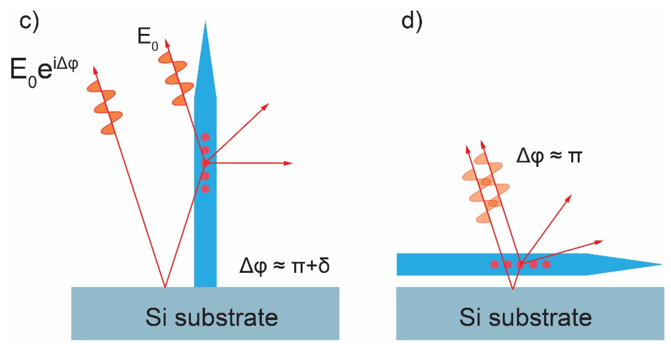
Finally, we should note that there is a discrepancy between an experimentally observed two order of magnitude difference of intensities of emitted radiation in “axial” and “radial” directions of emission. It can be seen from
Figure 4 that the difference of intensities of emission in “axial” and radial directions do not exceed one order of magnitude.
To explain two orders of magnitude differences in intensity, one should seek for additional reasons. One possible explanation could be based on negative interference of the wave, emitted in particular in the radial direction, and toward the substrate, and is then reflected from the substrate in the direction of the first wave. Reflection from the substrate gives the phase a shift near p, and two waves weaken each other, as shown in
Figure 1d. On other hand, the vertical alignment of NW, the phase shift between the wave emitted upward, and the wave emitted toward the substrate and reflected from it are about the same, and the two waves do not experience a negative interference. A qualitative numerical analysis of these effects is provided is
Supplementary Materials Section S3. It can be seen that the direction-dependent modification of the emission probability together with the negative interference (in the case of lying NW) of the waves emitted by QD outward from the substrate, emitted toward the substrate and reflected back (see
Figure S6 of Supplementary Materials), can explain the observed differences in the emission intensity.


 ,
, 