Abstract
Chemically vapor-deposited silicon carbide (CVD-SiC) is a high-performance material that possesses excellent mechanical, chemical, and electrical properties, making it highly promising for components in the semiconductor, aerospace, and automotive industries. However, its inherent hardness and brittleness present significant challenges to precision machining, thereby hindering the commercialization of reliable, high-precision parts. Therefore, the application of CVD-SiC in fields that require ultra-precision shaping and nanometric surface finishing necessitates the exploration of machining methods specifically tailored to the material’s unique characteristics. This paper presents a comprehensive review of CVD-SiC machining—from traditional mechanical approaches to advanced hybrid and high-energy techniques—aimed at overcoming machining limitations from its material properties and achieving high-efficiency and nanometric-quality machining. The study discusses various grinding tools designed for superior surface finishing and efficient material removal, as well as machining techniques that utilize micro-scale removal mechanisms for ductile regime machining. Looking ahead, the integration of AI-based process optimization with enhanced machining methods is expected to fully exploit the superior properties of CVD-SiC and broaden its industrial application as a high-performance material.
1. Introduction
CVD-SiC (Chemically vapor-deposited silicon carbide) has been attracting increasing attention across various fields due to its outstanding properties, including high strength, extreme hardness, low thermal expansion coefficient, excellent thermal conductivity, and superior chemical and radiation resistance [1,2,3]. Its value and utility are particularly evident in the semiconductor, aerospace, and defense industries, where the ultra-precision machining of high-performance components has become crucial. Applications of CVD-SiC in ultra-precision semiconductor jigs, optical mirrors, and aerospace optical components require extremely high shape accuracy and nanometric surface quality. For example, the continuous enlargement of optical lenses and mirrors for space observation to enhance image resolution demands advanced nano-finishing technology for ultra-large, flat surfaces, as well as materials that can withstand extreme environments such as space [4,5]. The excellent thermomechanical and chemical stability of CVD-SiC enhances its versatility, while its lightweight nature allows significant weight reduction for components of identical geometry. These attributes make it a key material for improving the performance of satellite structures and high-precision optical systems. CVD-SiC exhibits an exceptionally dense, nearly single-crystalline microstructure, achieving purity levels exceeding 99.999%. Its uniform atomic-bonding structure imparts outstanding hardness and strength; however, these same characteristics also make it extremely difficult to achieve defect-free surface quality during machining. Due to its high brittleness, the risks of cracking and fracture increase during processing, while its chemical inertness results in poor reactivity to chemical-based machining. Therefore, an in-depth understanding of machining methods tailored to the intrinsic material characteristics of CVD-SiC is essential for manufacturing components that demand high shape precision and nanometric surface finishes [6]. Among traditional mechanical machining techniques, polishing offers superior shape precision and surface smoothness but suffers from an extremely low Material Removal Rate (MRR), making it time-consuming. Grinding provides a higher MRR and good dimensional accuracy, yet issues such as wheel loading and uncontrolled cutting pressure often lead to brittle fractures. In addition, grinding wheel wear necessitates periodic dressing and replacement, increasing processing time and complexity. To address these challenges, Electrolytic In-Process Dressing (ELID) grinding was developed. This method allows continuous in situ dressing of the grinding wheel, maintaining low and stable cutting pressure, thereby minimizing the risk of cracking while achieving high efficiency and nanometric surface quality. High-energy machining techniques, such as ion beam machining and laser processing, also enable high shape precision and are suitable for complex geometries, micro-holes, and deep grooves, offering a high processing speed. However, thermal damage and surface degradation in the Heat-Affected Zone (HAZ) hinder the realization of nanometric finishing through laser machining, often requiring additional post-processing. Hybrid machining approaches combining chemical assistance and ultrasonic vibration have been developed to enhance surface finish and compensate for the low MRR of mechanical methods. Nevertheless, the extreme chemical and structural stability of CVD-SiC still limits the effectiveness of chemical polishing, leaving challenges in achieving true nano-scale surface finishes. Despite its exceptional potential and multifunctional properties, the commercialization of CVD-SiC remains difficult due to its inherent machining complexity. These developments motivate a need for integrated review. This paper provides a comprehensive review of existing CVD-SiC fabrication and machining technologies—including mechanical and high-energy-based processes—and discusses their limitations and challenges. Finally, it explores future research directions, focusing on AI-assisted ultra-precision machining control and process optimization as a pathway toward overcoming current limitations and realizing the full potential of CVD-SiC.
2. Characteristics of CVD-SiC
SiC can generally be classified into three major fabrication methods: reaction bonding (RB-SiC), pressureless sintering (S-SiC), and chemical vapor deposition (CVD-SiC). The specific manufacturing method determines the resulting microstructural and mechanical properties, which in turn influence the machinability and surface integrity of the material. Table 1 summarizes the key differences in mechanical properties among these fabrication techniques [7]. Reaction bonding is performed by infiltrating a carbon or carbon/SiC-based preform with molten silicon through capillary pressure. This process yields a relatively dense SiC composite while preserving the original shape and dimensional accuracy of the molded preform. In contrast, pressureless sintering achieves densification via self-diffusion and particle rearrangement at elevated temperatures without external pressure. This mechanism promotes atomic or molecular migration, enabling particle bonding. Because temperature is the key process variable and the apparatus is relatively simple, this technique does not require complex equipment. However, reaction bonding may suffer from incomplete infiltration and compositional non-uniformity, leading to lower final density and poor control of microstructural uniformity, such as residual porosity. In pressureless sintering, the absence of external pressure can result in fine pores, and the use of sintering additives may leave impurities that reduce the purity and reliability of the final product. To overcome these material limitations, recent research has focused on ultra-high-purity SiC synthesis and process refinement using Physical Vapor Transport (PVT) and High-Temperature Chemical Vapor Deposition (HTCVD) techniques. CVD-SiC is synthesized by reacting silicon- and carbon-containing precursor gases at high temperature, resulting in the deposition of a dense, high-purity SiC layer onto a substrate surface, as schematically shown in Figure 1. The CVD process enables near-theoretical density, uniform coating over complex geometries, and precise compositional control. During deposition, SiC typically forms a columnar microstructure, because atoms on the substrate surface preferentially grow in the direction normal to the substrate plane, producing elongated grains [8]. By comparison, RB-SiC and S-SiC exhibit polycrystalline and multiphase microstructures, which are often inhomogeneous due to the coexistence of various phases and residual impurities. In contrast, CVD-SiC predominantly consists of β-SiC (3C-SiC polytype) with a Face-Centered Cubic (FCC) lattice, characterized by a highly regular and repetitive atomic arrangement. This structural uniformity ensures excellent crystallographic continuity across grain boundaries, as illustrated in Figure 2, resulting in reduced defect formation and superior surface quality. The strong covalent bonds and high degree of atomic ordering in this structure significantly enhance resistance to external shock, abrasion, and corrosion, ensuring thermal and mechanical stability even under severe environments such as high-temperature, high-pressure, and chemically reactive atmospheres.

Table 1.
Comparison of the mechanical properties of CVD-SiC, S-SiC, and RB-SiC.
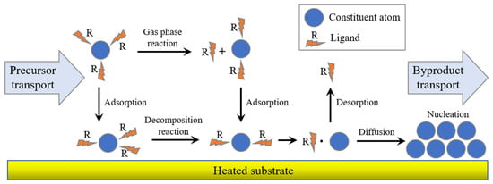
Figure 1.
Basic steps in the fabrication of CVD-SiC.
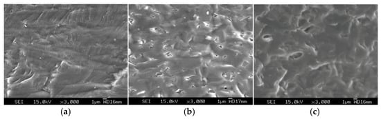
Figure 2.
SEM microstructures of SiC types: (a) CVD-SiC; (b) S-SiC; (c) RB-SiC *. * Park et al., 2017 [7].
Pickering et al. [9] experimentally confirmed the superior optical suitability of CVD-SiC, attributing it to its single-phase, high-purity, and high-density composition, which provides excellent thermo-mechanical and optical characteristics. Furthermore, the uniform columnar microstructure of CVD-SiC results in properties distinctly different from those of RB-SiC and S-SiC. While this regular microstructure improves mechanical and optical performance, it also increases machining difficulty, implying that conventional cutting or grinding methods are insufficient and that the material is highly sensitive to process parameters [10].
3. Mechanical Machining Methods for CVD-SiC
Mechanical machining is commonly employed for processing hard and brittle ceramics, including CVD-SiC, where fine abrasive grains are utilized to achieve the desired surface finish. However, due to the material’s intrinsic hardness and brittleness, even when fine abrasives are used, the MRR remains extremely low, and rapid tool wear is inevitable. Moreover, CVD-SiC’s susceptibility to brittle fracture poses significant challenges in maintaining surface integrity, as microcracks and Subsurface Damage (SSD) can easily occur. To ensure high-quality surface finishing, mechanical machining methods are generally categorized into two types based on the abrasive mechanism: loose abrasive machining and fixed abrasive machining. Loose abrasive machining, schematically illustrated in Figure 3, is primarily applied for the precision finishing of glass, ceramics, and semiconductor wafers.
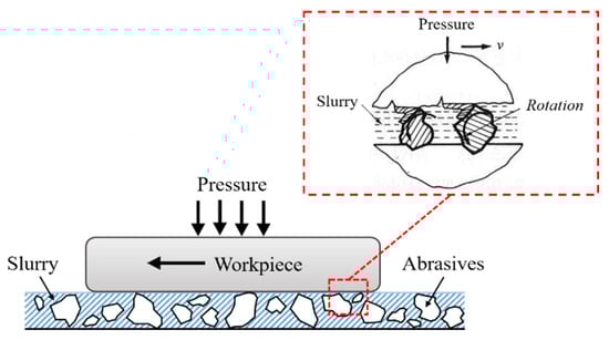
Figure 3.
Schematic of the loose abrasive machining.
This method removes material through the relative motion of the workpiece under pressure using a mixture of abrasive particles and liquid (slurry), or by vibrational energy that accelerates abrasive grains, inducing localized brittle fracture upon impact. In contrast, fixed abrasive machining (Figure 4) utilizes abrasive particles bonded to a pad or wheel, which move along a fixed path during machining, thereby enabling consistent material removal. This approach is advantageous for optical and semiconductor applications requiring high repeatability and dimensional accuracy. However, since conventional polishing involves a trade-off between removal rate and surface quality, the ultra-precision finishing of CVD-SiC coatings typically requires multi-step hybrid polishing sequences that combine both fixed- and loose abrasive polishing.
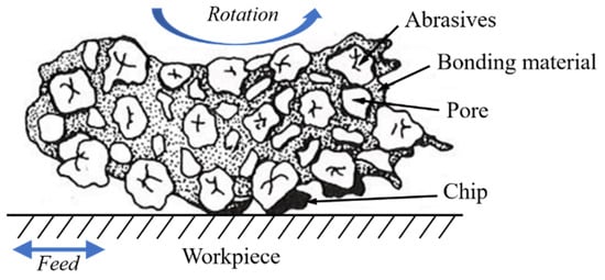
Figure 4.
Schematic of the fixed abrasive machining.
3.1. Loose Abrasive Machining
Loose abrasive machining methods, such as lapping and polishing, have long been used for mirror finishing of CVD-SiC. However, conventional approaches exhibit extremely low MRRs, necessitating prolonged machining times. Moreover, uneven slurry distribution between the pad and workpiece, caused by the continuous supply of large slurry volumes under pressure, often results in non-uniform contact pressure and uneven surface textures. Environmental issues related to slurry waste and wastewater treatment also limit the feasibility of these processes for mass production. To address these limitations, a novel polishing approach using a Magnetic Compound Fluid (MCF) slurry was introduced by Shimada et al. [11], and later applied to CVD-SiC nano-finishing by Wu et al. [12]. The MCF slurry is synthesized by combining Magnetic Fluid (MF) and Magnetorheological Fluid (MRF) in a shared solvent, to which abrasive particles and α-cellulose fibers are added. This formulation generates high magnetic pressure and viscosity, allowing contact-free, magnetically controlled surface finishing, as shown in Figure 5. A rotating magnetic field regulates both the distribution and movement of the slurry, ensuring a uniform polishing pressure without continuous replenishment. Experimental results revealed optimal process parameters, including rotational speed and slurry composition, that minimized surface roughness to below 2 nm Ra, confirming the effectiveness of MCF slurry for nanometric surface finishing of CVD-SiC.
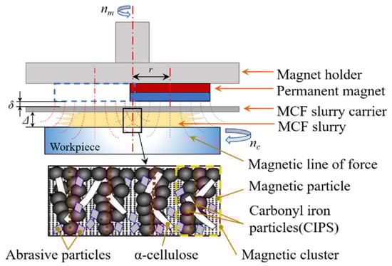
Figure 5.
Schematic of the polishing principle with Magnetic Compound Fluid (MCF) slurry.
Hur et al. [13] further enhanced conventional machining by applying ultrasonic vibration during Poly-Crystalline Diamond (PCD) drilling of CVD-SiC. Using a 20 kHz ultrasonic micro-machine with a water–diamond powder slurry, they investigated the effects of vertical load on chipping behavior, surface roughness, and hole quality. The results confirmed a reduction in chipping and improved surface finish, demonstrating that ultrasonic-assisted machining can significantly suppress brittle fracture. Future research should focus on optimizing vibration parameters, slurry type and concentration, and tool geometry for improved process stability. Seo et al. [14,15] developed an Orthogonal Velocity Tool (OVT) for mirror polishing of CVD-SiC surfaces. As depicted in Figure 6a, the OVT system consists of a tool head, slurry supply module, and electronic control unit, incorporating a simplified two-axis rotation system (Figure 6b) to generate an orthogonal velocity field. This design minimizes directional polishing marks, and through real-time pressure monitoring via a load cell, enables adaptive control of contact force and dwell time. Experimental validation confirmed that pseudo-Gaussian tool influence functions (TIFs) with ~89.7% repeatability were achieved. However, as workpiece size increases, the pressure distribution across the contact area becomes more complex, suggesting that enhanced multi-axis motion control is necessary for large-aperture surface optimization. Although loose abrasive techniques provide high-quality finishing, their low MRR and long processing time remain key challenges for scalable, cost-effective production.
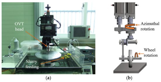
Figure 6.
Orthogonal Velocity Tool (OVT): (a) Polishing machine comprising OVT head and slurry feeding subsystems; (b) Schematic of the OVT principle.
3.2. Fixed Abrasive Machining
CVD-SiC exhibits an extremely low polishing rate, with a Preston coefficient roughly one-twentieth that of optical glass under identical conditions. Bifano et al. [16] pioneered the ductile regime grinding technique, exploiting the localized ductile behavior of ceramics when the Depth of Cut (DOC) is sufficiently small. Using a resin-bonded diamond wheel, they demonstrated that plastic flow dominates material removal under these conditions. When the DOC is below the critical depth for brittle-to-ductile transition, the localized stress concentration at the tool edge exceeds the material’s fracture strength, leading to atomic bond rearrangement rather than crack propagation. The resulting surface exhibited a roughness of 0.55 nm RMS over a 50 µm scan, confirming the feasibility of ultra-precision grinding for CVD-SiC optical mirrors. Bhattacharya et al. [17] simulated Single Point Diamond Turning (SPDT) on CVD-SiC through scratch testing to identify the Ductile-to-Brittle Transition (DBT) depth. They achieved a final surface roughness of 8–20 nm Ra without post-polishing, proving that ductile-mode SPDT can significantly reduce process steps and cost. Ravindra et al. [18,19] expanded upon this work by performing multi-pass ductile SPDT on polycrystalline CVD-coated SiC (Figure 7), achieving surface improvement from 1.23 µm Ra to 88 nm Ra with no SSD or fracture marks. However, tool wear increased notably at lower feed rates, reducing process efficiency, suggesting a need for new tool materials and optimized coolant systems.
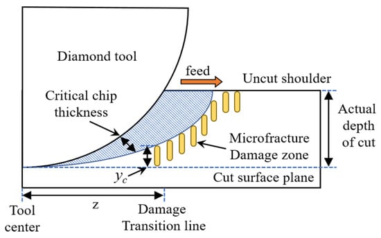
Figure 7.
Model of the ductile regime machining for a damage-free surface.
Ohmori et al. [20] later applied ELID grinding to fabricate ultra-precision CVD-SiC X-ray mirrors (Figure 8). This technique continuously renews the wheel surface via electrochemical oxidation, maintaining low cutting pressure and stable removal. The resulting mirror exhibited 0.0028 µm Ra surface roughness and a precisely controlled radius of curvature, demonstrating that ELID effectively mitigates tool wear and enables stable high-precision machining. To validate ELID performance, Zhang et al. [21,22] compared ELID with conventional dressing methods, finding similar surface roughness (9.8 nm Ra vs. 11.4 nm Ra) using a #4000 cast iron-bonded diamond wheel, but a higher ductile removal ratio in ELID. Thus, ELID provides superior process stability and quality, particularly for fine-grain diamond wheels. Recently, Ao et al. [23] combined ELID pre-treatment with Fixed Softer-Than-Diamond Abrasive (FSTDA) grinding, comparing poly-CeO2, Al2O3, and poly-SiC abrasives. They found strong correlations between abrasive hardness and final surface roughness, with FSTDA achieving superior step suppression and planarization versus CMP. However, since oxide film formation in ELID depends heavily on electrical parameters and grinding fluid chemistry, further optimization of oxide layer composition and thickness control is essential.
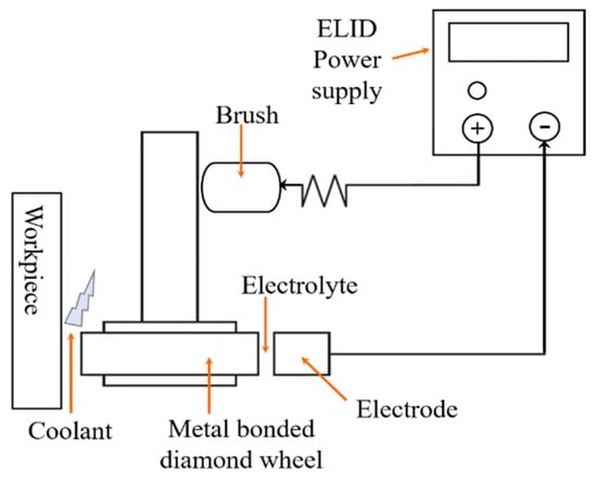
Figure 8.
Schematic of the Electrolytic In-Process Dressing (ELID) principle.
Ongoing innovations include Single-Crystal Diamond (SCD) and Nano-Polycrystalline Diamond (NPCD) micro-milling tools for CVD-SiC molds used in aspheric glass lens fabrication [24], Shape Adaptive Grinding (SAG) tools for freeform optics [25], and 5-axis ultra-precision grinding systems for synchrotron radiation mirrors [26,27]. The SAG method (Figure 9) uses an elastically deformable tool that conforms to the surface curvature, achieving <0.4 nm Ra roughness and MRR up to 100 mm3/min. Similarly, 5-axis grinding attained 3.3 nm RMS roughness and 750 nm form accuracy, satisfying X-ray mirror requirements without final polishing, thus drastically reducing process time.
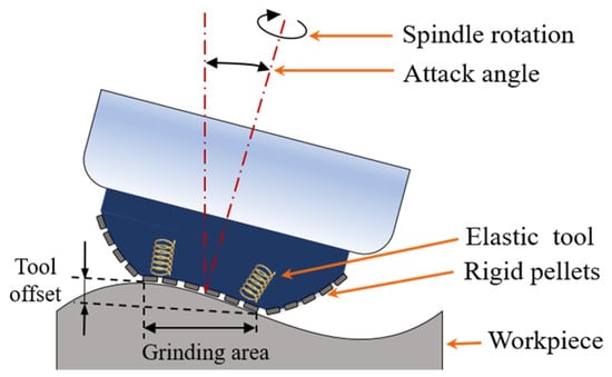
Figure 9.
Schematic of the Shape Adaptive Grinding (SAG).
4. High-Energy Machining Methods
The high hardness (~30 GPa) and low fracture toughness of CVD-SiC pose severe challenges for conventional contact machining as tool wear, chipping, and residual stress are common. To overcome these issues, hybrid high-energy, non-contact machining methods have been developed. Fawcett et al. [28] first applied neutral Ion Beam Figuring (IBF) (Figure 10) for CVD-SiC mirror finishing. In IBF, accelerated inert gas ions bombard the surface, causing atomic-scale sputtering removal and enabling nanometer-level form correction. The process induces minimal thermal effects and avoids SSD, making it ideal for thin, lightweight optics. However, when applied to pre-polished or micro-ground CVD-SiC, surface roughness increased from ~5 nm to ~140 nm RMS, as residual SSDs from earlier steps were exposed by ion etching. Thus, minimizing SSD during pre-machining and precise ion-beam depth control are critical for effective IBF. Gailly et al. [29,30] further optimized IBF by adjusting beam energy, ion type, and beam profile, reducing roughness from 243 nm RMS to 13 nm RMS, with End-Hall sources increasing removal efficiency compared to Kaufman sources. Nonetheless, the etch rate remains low, requiring parameter optimization for removal rate and surface uniformity.
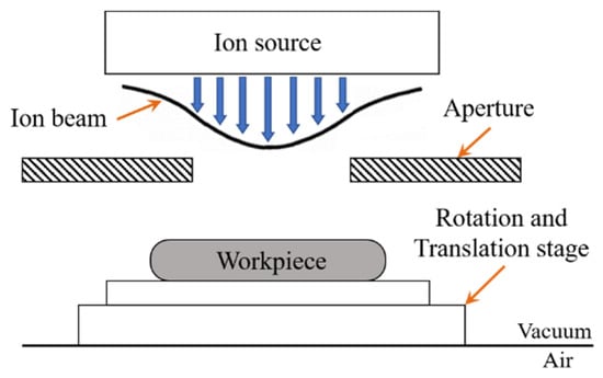
Figure 10.
Schematic of the Ion Beam Figuring (IBF) process.
Nianhui et al. [31] proposed a hybrid polishing–IBF sequence using Magnetorheological Finishing (MRF) to measure SSD depth after each step and adjust removal thickness accordingly. This deterministic hybrid approach achieved super-smooth reflectors within coating tolerance limits. For even finer finishing, Deng et al. [32] developed a Plasma Chemical Vaporization Machining (PCVM)–Plasma-Assisted Polishing (PAP) hybrid process (Figure 11). PCVM, a dry, non-contact plasma etching technique, removes SSD layers, followed by PAP, which uses reactive plasma and micro-abrasives to form and remove a soft oxide layer. This method yielded 0.69 nm RMS surface roughness, outperforming CMP while being environmentally cleaner. However, process optimization of CF4/O2 ratios in PCVM and thermal-resistant pad materials in PAP remains necessary [33]. Ravindra et al. [34] investigated Laser Ablation–SPDT hybrid machining, combining localized thermal softening by laser with ductile-mode turning. This reduced surface roughness by 50% and peak-to-valley variation by 75%, but laser-induced thermal cracking accelerated tool wear. Optimal feed rate, laser power, and overlap conditions are crucial to balancing efficiency and surface integrity. These developments highlight the importance of intelligent optimization frameworks for multi-parameter control. The main mechanisms of the high-energy-applied machining methods are summarized in Table 2.
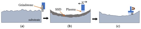
Figure 11.
Steps in the damage-free finishing process for CVD-SiC: (a) Mechanical machining; (b) Plasma Chemical Vaporization Machining (PCVM); (c) Plasma-Assisted Polishing (PAP).
Table 2.
Description of high-energy application machining methods.
5. AI-Based Ultra-Precision Control Technology
In recent years, Artificial Intelligence (AI) has begun to revolutionize materials processing, significantly improving efficiency, precision, and process reliability. For hard and brittle materials such as CVD-SiC, conventional control systems are often inadequate to manage complex machining dynamics and ensure consistent reproducibility. Therefore, AI-based ultra-precision control has emerged as a promising approach for multi-dimensional analysis, prediction, and optimization of intricate machining parameters. This paradigm can potentially reduce process difficulty and establish reliable machining technologies for next-generation precision manufacturing. Historically, AI applications relied primarily on real-time sensor feedback and empirical process data, adopting knowledge-based expert systems, probabilistic inference, and early-generation neural networks [35]. However, recent advances have expanded to include Machine Learning (ML), Deep Learning (DL), and Reinforcement Learning (RL) frameworks, which enable data-driven predictive modeling and self-optimizing control of machining processes [36]. These developments have allowed AI to perform parameter prediction, process simulation, defect detection, and adaptive optimization during ultra-precision machining operations. Abdullah et al. [37] demonstrated the effectiveness of Genetic Algorithms (GA) and Ant Colony Optimization (ACO) in generating optimal tool paths for CNC drilling. Their MATLAB simulations showed that AI-optimized paths were shorter and more efficient than those generated by commercial CAD/CAM software, indicating that AI can extend tool life, reduce surface defects, and accelerate optimization cycles. Markopoulos et al. [38] developed a hybrid Finite Element Method–Artificial Neural Network (FEM–ANN) model to predict thermal damage and microstructural evolution during grinding. Although CVD-SiC exhibits excellent heat resistance, localized high temperatures from extreme friction can create a HAZ, decomposing SiC into silicon and carbon. The subsequent graphitization of carbon decreases hardness and wear resistance, while non-uniform grain refinement and residual stresses degrade mechanical integrity. Their FEM-ANN model effectively predicted maximum surface temperatures and load distribution, providing a valuable tool for damage control and process stabilization. From a sustainability perspective, AI-based energy optimization is gaining increasing attention. Pawanr and Gupta [39] reviewed methods to enhance energy efficiency in machining, reporting potential reductions up to 45% through energy-efficient design, 40% via cutting parameter optimization, and 50% through optimized tool paths. Moreover, AI-based process sequencing yielded an additional 20–30% improvement in overall energy efficiency, reinforcing the potential of AI for green and sustainable manufacturing. In addition, Soori et al. [40] comprehensively reviewed AI and ML applications in CNC machining, covering tool wear prediction, cutting force modeling, maintenance scheduling, surface quality prediction, and energy consumption forecasting. They highlighted that ML-based energy prediction models exhibit higher reliability and accuracy than traditional empirical methods. Although challenges remain in implementing advanced ML frameworks for real-time machining, the adoption of smart CNC systems based on self-optimization algorithms is expected to transform conventional machining into intelligent manufacturing [41]. Ullrich et al. [42] emphasized the necessity of Multi-Objective Optimization (MOO) for achieving global performance enhancement in machining systems. Their review revealed that deep learning is the most frequently utilized ML method, and that surface quality parameters (e.g., form accuracy and roughness) are the dominant performance metrics. They also discussed key challenges, such as mathematical complexities in MOO, real-time predictive modeling, and the gap between optimized models and industrial implementation. To overcome these, the authors proposed hybrid optimization frameworks integrating Support Vector Machines (SVM), Decision Trees (DT), Random Forests (RF), and Evolutionary Algorithms (EA) to improve accuracy and generalization in machining optimization. The integration of AI with robotics and autonomous manufacturing systems represents the next frontier in ultra-precision machining of hard and brittle materials like CVD-SiC. Robots provide high flexibility and multi-axis adaptability, but challenges remain [43]: (1) in low-MRR operations, excessive flexibility complicates path programming and automation; (2) in high-MRR operations, low structural stiffness induces vibrations that degrade precision. Recent studies have utilized ML and DL to predict and compensate for these vibrations. For instance, ANN and Support Vector Regression (SVR) models can estimate real-time deviations based on joint torque, temperature, and force data, allowing in-process error correction. Similarly, Recurrent Neural Networks (RNN) and Long Short-Term Memory (LSTM) architectures have been used to analyze vibration sequences and prevent equipment failure through early anomaly detection [44,45].
The machining technology using AI can be utilized to control the process by determining the optimal machining conditions based on trained data and the characteristics of the material. In particular, hard and brittle materials such as ceramics face difficult challenges, including the need to improve machinability, achieve nanoscale surface quality, and prevent fracture during machining. Therefore, if the machining conditions are controlled using AI to maintain the highest material removal rate and a consistent machining pressure, many of these issues can be resolved. Ultimately, the synergy between AI, ML, and robotic systems is expected to provide self-optimizing, adaptive machining environments, enabling the high repeatability, stability, and precision required for next-generation CVD-SiC component fabrication. Such integration will transform conventional machining into intelligent, adaptive manufacturing ecosystems.
6. Conclusions
This review comprehensively examined mechanical, hybrid, and high-energy machining processes for CVD-SiC, a material characterized by exceptional hardness, brittleness, and thermal stability. Loose abrasive and fixed abrasive techniques were compared, and hybrid approaches were highlighted for overcoming the inherent challenges of low MRRs and surface defects. Methods such as ductile regime SPDT, ELID grinding combined with FSTDA, and SAG have demonstrated substantial progress toward achieving super-smooth, damage-free surfaces. High-energy-assisted machining methods—including IBF, PCVM, PAP, and Laser–SPDT hybrids—have shown promise in reducing micro-cracks, residual stress, and tool wear, while enhancing form accuracy and optical performance. However, achieving reproducible sub-nanometer roughness across large apertures remains a key challenge. Each technique requires precise control of process parameters to balance removal rate, thermal effects, and surface quality. Future research should emphasize systematic hybridization strategies, integrating multiple machining principles to exploit synergistic effects at both macroscopic and atomic scales. Looking ahead, AI-driven ultra-precision control is poised to redefine the machining landscape for hard materials such as CVD-SiC. By integrating ML, deep learning, and reinforcement learning into autonomous control systems, it will be possible to analyze, predict, and optimize complex process interactions in real time. This advancement will reduce machining difficulty, improve repeatability, and shorten process cycles, ultimately paving the way for the widespread commercialization of CVD-SiC as a core high-performance material in semiconductor, aerospace, and defense industries.
Funding
This research was supported by the Korea Research Institute for Defense Technology Planning and Advancement (22–107-I00–003) funded by the Korea Defense Acquisition Program Administration (DAPA).
Institutional Review Board Statement
Not applicable.
Informed Consent Statement
Not applicable.
Data Availability Statement
The original contributions presented in this study are included in the article. Further inquiries ca be directed to the corresponding author.
Conflicts of Interest
The authors declare no conflicts of interest.
References
- Goela, J.S.; Pickering, M.A.; Taylor, R.L.; Murray, B.W.; Lompado, A. Properties of chemical-vapor-deposited silicon carbide for optics applications in severe environments. Appl. Opt. 1991, 30, 3166–3175. [Google Scholar] [CrossRef]
- Mubina, S.; Khanra, A.K.; Saha, B.P. Enhancement of oxidation resistance of CVD SiC coated Cf/C-SiC hybrid composite tubes processed through Si-infiltration. J. Alloys Compd. 2020, 826, 154107. [Google Scholar] [CrossRef]
- Seshadri, A.; Phillips, B.; Shirvan, K. Impact of nuclear environment on hydrothermal corrosion and silica transport for CVD SiC in light water reactors. J. Nucl. Mater. 2021, 556, 153155. [Google Scholar] [CrossRef]
- Zhang, X.; Hu, H.; Wang, X.; Luo, X.; Zhang, G.; Zhao, W.; Wang, X.; Liu, Z.; Xiong, L.; Qi, E.; et al. Challenges and strategies in high-accuracy manufacture of the world’s largest SiC aspheric mirror. Light Sci. Appl. 2022, 11, 310. [Google Scholar] [CrossRef] [PubMed]
- Tayaramma, D.P.V.J.; Rao, B.V.; Rudraswamy, B.; Venkateswaran, B.; Sriram, K.V. Optical polishing and characterization of chemical vapour deposited silicon carbide mirrors for space applications. J. Opt. 2022, 52, 969–983. [Google Scholar] [CrossRef]
- Bae, J.I.; Lee, H.B.; Kim, J.W.; Lee, K.M.; Kim, M.W. Development of a Silicon Carbide Large-aperture Optical Telescope for a Satellite. Korean J. Opt. Photonics 2022, 33, 74–83. [Google Scholar]
- Park, H.K. A Study on the Deposition and Grinding Characteristics of CVD-SiC for Semiconductor Process. Ph.D. Thesis, Kumoh National Institute of Technology, Gumi, Republic of Korea, 2017. [Google Scholar]
- Cheng, D.J.; Shyy, W.J.; Kuo, D.H.; Hon, M.H. Growth characteristics of CVD beta—Silicon carbide. J. Electrochem. Soc. 1987, 134, 3145. [Google Scholar] [CrossRef]
- Pickering, M.A.; Taylor, R.L.; Keeley, J.T.; Graves, G.A. Chemically vapor—Deposited silicon carbide (SiC) for optical applications. Nucl. Instrum. Methods Phys. Res. A 1990, 291, 95–100. [Google Scholar] [CrossRef]
- Zhou, J.; Lin, B.; Xue, J.; Li, S.; Liao, Y.; Zhao, P.; Sui, T. Damage characteristics and material removal mechanisms of CVD—iC in nanotests: A comparative with sintered SiC. Int. J. Refract. Met. Hard Mater. 2023, 118, 106460. [Google Scholar] [CrossRef]
- Shimada, K.; Fujita, T.; Oka, H.; Kamiyama, S.; Akagami, Y. Hydrodynamic and magnetized characteristics of MCF (magnetic compound fluid). Trans. Jpn. Soc. Mech. Eng. Ser. B 2001, 67, 3034–3040. [Google Scholar] [CrossRef]
- Wu, Y.; Wang, Y.; Fujimoto, M.; Nomura, M. Nano-precision polishing of CVD SiC using MCF (magnetic compound fluid) slurry. J. Korean Soc. Manuf. Technol. Eng. 2014, 23, 547–554. [Google Scholar] [CrossRef]
- Hur, C. A Study on Drilling Technology for Silicon Carbide. Master’s Thesis, Kumoh National Institute of Technology, Gumi, Republic of Korea, 2007. [Google Scholar]
- Seo, H.; Han, J.Y.; Kim, S.W.; Seong, S.; Yoon, S.; Lee, K.; Lee, H. Material removal characteristics of orthogonal velocity polishing tool for efficient fabrication of CVD SiC mirror surfaces. In Optical Manufacturing and Testing XI; SPIE: Bellingham, WA, USA, 2015; Volume 9575, pp. 115–124. [Google Scholar]
- Seo, H.; Han, J.Y.; Kim, S.W.; Seong, S.; Yoon, S.; Lee, K.; Hong, J.; Lee, H.; Bok, M. Novel orthogonal velocity polishing tool and its material removal characteristics from CVD SiC mirror surfaces. Opt. Express 2016, 24, 12349–12366. [Google Scholar] [CrossRef]
- Bifano, T.; Yi, Y.; Kahl, K. Fixed abrasive grinding of CVD SiC mirrors. Precis. Eng. 1994, 16, 109–116. [Google Scholar] [CrossRef]
- Bhattacharya, B.; Patten, J.A.; Jacob, J. Single point diamond turning of CVD coated silicon carbide. In Proceedings of the 2006 ASME International Conference on Manufacturing Science and Engineering, Ypsilanti, MI, USA, 8–11 October 2006. [Google Scholar]
- Ravindra, D.; Patten, J. Ductile regime single point diamond turning of CVD-SiC resulting in an improved and damage-free surface. In Proceedings of the 4th International Conference on Recent Advances in Materials, Minerals & Environment and 2nd Asian Symposium on Materials & Processing, Penang, Malaysia, 1–3 June 2009. [Google Scholar]
- Ravindra, D.; Patten, J. Improving the Surface Roughness of a CVD Coated Silicon Carbide Disk by Performing Ductile Regime Single Point Diamond Turning. In Proceedings of the 2008 International Manufacturing Science and Engineering Conference, Evanston, IL, USA, 7–10 October 2008. [Google Scholar]
- Ohmori, S.; Moriyasu, S.; Uehara, Y.; Yamagata, Y.; Hayashi, W.; Makinouchi, A. CVD-SiC X-ray Mirror of Ultraprecision Grinding with ELID (Electrolytic In-Process Dressing). J. Jpn. Soc. Mech. Eng. 2000, 504, 123–134. [Google Scholar]
- Zhang, C.; Kato, T.; Li, W.; Ohmori, H. A Comparative Study: Surface Characteristics of CVD-SiC Ground with Cast Iron Bond Diamond Wheel. Int. J. Mach. Tools Manuf. 2000, 40, 527–537. [Google Scholar] [CrossRef]
- Zhang, C.; Ohmori, H.; Kato, T.; Morita, N. Evaluation of surface characteristics of ground CVD-SiC using cast iron bond diamond wheels. Precis. Eng. 2001, 25, 56–62. [Google Scholar] [CrossRef]
- Ao, X.; Kurokawa, S.; Hayashi, T.; Ohmori, H.; Jia, C. Super-smooth processing of CVD-SiC using combined electrolytic in-process dressing grinding and fixed softer-than-diamond abrasive grinding. Int. J. Adv. Manuf. Technol. 2025, 139, 2803–2821. [Google Scholar] [CrossRef]
- Suzuki, A.; Okada, M.; Suzuki, H.; Fujii, K.; Itoh, Y.; Fukuda, T. Ultraprecision cutting of CVD-SiC by micro milling tool of diamond. In Proceedings of the 2019 JSPE Fall Conference, Nagoya, Japan, 9–11 September 2019. [Google Scholar]
- Beaucamp, A.; Namba, Y.; Combrinck, H.; Freeman, R. Shape Adaptive Grinding of CVD Silicon Carbide. CIRP Ann. 2014, 63, 317–320. [Google Scholar] [CrossRef]
- Namba, Y.; Suzuki, H. Surface-figuring CVD-SiC mirrors with a five-axis-control ultraprecision grinding machine. In Materials, Manufacturing, and Measurement for Synchrotron Radiation Mirrors; SPIE: Bellingham, WA, USA, 1997; Volume 3152, pp. 27–34. [Google Scholar]
- Namba, Y.; Kobayashi, H.; Suzuki, H.; Yamashita, K.; Taniguchi, N. Ultraprecision surface grinding of chemical vapor deposited silicon carbide for X-ray mirrors using resinoid-bonded diamond wheels. CIRP Ann. 1999, 48, 277–280. [Google Scholar] [CrossRef]
- Fawcett, S.C.; Drueding, T.W.; Bifano, T.G. Neutral ion figuring of chemical vapor deposited SiC. Opt. Eng. 1994, 33, 967–974. [Google Scholar] [CrossRef]
- Gailly, P.; Collette, J.P.; Fleury-Frenette, K.; Jamar, C. Ion beam figuring of CVD silicon carbide mirrors. In Proceedings of the International Conference on Space Optics 2004, Toulouse, France, 30 March–2 April 2004. [Google Scholar]
- Gailly, P.; Fleury-Frenette, K.; Lecat, J.H.; Collette, J.P.; Defise, J.M. Ion beam figuring for precision optics. SPIE Newsroom 2008, 10, 1106. [Google Scholar] [CrossRef]
- Nianhui, K.; Shengyi, L.; Ziwen, Z.; Yifan, D. High-precision and Super-smooth Fabrication of CVD SiC Flat Reflecting Mirror. China Mech. Eng. 2009, 20, 69–73. [Google Scholar]
- Deng, H.; Endo, K.; Yamamura, K. Damage-free finishing of CVD-SiC by a combination of dry plasma etching and plasma-assisted polishing. Int. J. Mach. Tools Manuf. 2017, 115, 38–46. [Google Scholar] [CrossRef]
- Sun, R.; Yang, X.; Ohkubo, Y.; Endo, K.; Yamamura, K. Optimization of Gas Composition Used in Plasma Chemical Vaporization Machining for Figuring of Reaction-Sintered Silicon Carbide with Low Surface Roughness. Sci. Rep. 2018, 8, 2505. [Google Scholar] [CrossRef] [PubMed]
- Ravindra, D.; Patten, J.; Jacobsen, R. Hybrid laser ablation-single point diamond turning machining process for CVD-silicon carbide ceramics. Int. J. Manuf. Res. 2013, 8, 227–249. [Google Scholar] [CrossRef]
- Park, K.S.; Kim, S.H. Artificial intelligence approaches to determination of CNC machining parameters in manufacturing: A review. Artif. Intell. Eng. 1998, 12, 121–134. [Google Scholar] [CrossRef]
- Yang, H.; Zheng, H.; Zhang, T. A review of artificial intelligent methods for machined surface roughness prediction. Tribol. Int. 2024, 199, 109935. [Google Scholar] [CrossRef]
- Abdullah, H.; Ramli, R.; Wahab, D.A.; Qudeiri, J.A. Simulation approach of cutting tool movement using artificial intelligence method. J. Eng. Sci. Technol. 2015, 10, 35–44. [Google Scholar]
- Markopoulos, A.P.; Kundrák, J. FEM/AI Models for the Simulation of Precision Grinding. Manuf. Technol. 2016, 16, 384–390. [Google Scholar] [CrossRef]
- Pawanr, S.; Gupta, K. A Review on Recent Advances in the Energy Efficiency of Machining Processes for Sustainability. Energies 2024, 17, 3659. [Google Scholar] [CrossRef]
- Soori, M.; Arezoo, B.; Dastres, R. Machine learning and artificial intelligence in CNC machine tools, A review. Sustain. Manuf. Serv. Econ. 2023, 2, 100009. [Google Scholar] [CrossRef]
- Li, A.; Zhou, J.; Niu, X.; Liu, Z.; Ma, Q.; Song, S.; Wang, M.; Hu, B. Advances and challenges in chemical mechanical polishing of silicon carbide: Materials, mechanisms, and future directions. J. Mater. Chem. C 2025, 13, 22921. [Google Scholar] [CrossRef]
- Ullrich, K.; von Elling, M.; Gutzeit, K.; Dix, M.; Weigold, M.; Aurich, J.C.; Wertheim, R.; Jawahir, I.S.; Ghadbeigi, H. AI-based optimisation of total machining performance: A review. CIRP J. Manuf. Sci. Technol. 2024, 50, 40–54. [Google Scholar] [CrossRef]
- Ji, W.; Wang, L. Industrial robotic machining: A review. Int. J. Adv. Manuf. Technol. 2019, 103, 1239–1255. [Google Scholar] [CrossRef]
- Knittel, D.; Makich, H.; Nouari, M. Milling diagnosis using artificial intelligence approaches. Mech. Ind. 2019, 20, 809. [Google Scholar] [CrossRef]
- Razak, N.H.; Rahman, M.M.; Noor, M.M.; Kadirgama, K. Artificial Intelligence Techniques for Machining Performance: A Review. In Proceedings of the 2nd National Conference in Mechanical Engineering Research and Postgraduate Studies (NCMER 2010), Kuantan, Malaysia, 3–4 December 2010. [Google Scholar]
Disclaimer/Publisher’s Note: The statements, opinions and data contained in all publications are solely those of the individual author(s) and contributor(s) and not of MDPI and/or the editor(s). MDPI and/or the editor(s) disclaim responsibility for any injury to people or property resulting from any ideas, methods, instructions or products referred to in the content. |
© 2025 by the authors. Licensee MDPI, Basel, Switzerland. This article is an open access article distributed under the terms and conditions of the Creative Commons Attribution (CC BY) license (https://creativecommons.org/licenses/by/4.0/).