Automated Detection and Classification of Defective and Abnormal Dies in Wafer Images

Department of Electrical Engineering, National United University, Miaoli 36063, Taiwan
Appl. Sci. 2020, 10(10), 3423; https://doi.org/10.3390/app10103423
Submission received: 6 April 2020
/
Revised: 6 May 2020
/
Accepted: 13 May 2020
/
Published: 15 May 2020
(This article belongs to the Section Electrical, Electronics and Communications Engineering)
Abstract
:Featured Application
This study presents a fully automated scheme for wafer inspection using scanning acoustic tomography images. Differing from traditional template-matching based methods, the proposed method involves a template extraction algorithm and a deep learning-based classification. This benefits the inspection process, making it more convenient and accurate.
Abstract
This article presents an automated vision-based algorithm for the die-scale inspection of wafer images captured using scanning acoustic tomography (SAT). This algorithm can find defective and abnormal die-scale patterns, and produce a wafer map to visualize the distribution of defects and anomalies on the wafer. The main procedures include standard template extraction, die detection through template matching, pattern candidate prediction through clustering, and pattern classification through deep learning. To conduct the template matching, we first introduce a two-step method to obtain a standard template from the original SAT image. Subsequently, a majority of the die patterns are detected through template matching. Thereafter, the columns and rows arranged from the detected dies are predicted using a clustering method; thus, an initial wafer map is produced. This map is composed of detected die patterns and predicted pattern candidates. In the final phase of the proposed algorithm, we implement a deep learning-based model to determine defective and abnormal patterns in the wafer map. The experimental results verified the effectiveness and efficiency of our proposed algorithm. In conclusion, the proposed method performs well in identifying defective and abnormal die patterns, and produces a wafer map that presents important information for solving wafer fabrication issues.
1. Introduction
Automated visual inspection (AVI) is a challenging domain in the automation industry and is widely applied to production lines for quality control. Systems used in the AVI typically involve fields such as mechanical and electrical engineering, optics, mathematics, and computer science. Image analytics plays an important role in the success of a visual inspection system. During the past few decades, numerous vision-based approaches and related techniques have been presented for solving problems in the semiconductor industry, and have been widely employed for detecting defects and anomalies in major semiconductor materials and products, such as wafers and chips. A large number of studies have been conducted, including vision algorithms, performance improvements, and hardware and software development. In this study, we focus on the defective pattern detection of wafers.
Various optical inspection approaches were reviewed in [1]; these approaches were categorized based on the inspection techniques and inspected products. The semiconductor fabrication process is typically divided into three main phases requiring different inspection algorithms. During the first phase, wafers are manufactured from raw materials using crystal growth, slicing, polishing, lapping, etching, and other steps. An integrated circuit (IC) pattern is then projected onto the wafer surface. During the second phase, a wafer acceptance test is applied to verify the effectiveness of all the individual ICs (also known as a die). Finally, the wafer is cut into chips, and the manufacturing process is completed through the packaging stage. A visual inspection is always applied during the defect detection for every die pattern prior to the IC packaging.
There has been a significant increase in the complexity of IC structures in recent years; this has increased the difficulty of die-scale wafer inspection. A template-based vision system for the inspection of a wafer die surface was presented in [2]. Schulze et al. [3] introduced an inspection technology based on digital holography, which records the amplitude and phase of the wave front from the target object directly to a single image acquired via a CCD camera. The technology was also proven to be effective for identifying defects on wafers. In [4], Kim and Oh proposed a method using component tree representations of scanning electron microscopy (SEM) images. However, their method has only been evaluated qualitatively. To conduct a quantitative assessment, a large dataset must be prepared by domain experts. A method employing a two-dimensional wavelet transform approach was developed to detect visual defects, such as particles, contamination, and scratches on wafers [5]. Magneto-optic imaging, which involves inducing eddy current into the target wafer, is used to inspect semiconductor wafers [6]. Moreover, an algorithm comprising noise reduction, image enhancement, watershed-based segmentation, and clustering strategy was presented.
Over the past few decades, scanning acoustic microscopes (SAMs) have been extensively utilized in the inspection of semiconductor products [7]. They are commonly used in non-destructive evaluations through a process called scanning acoustic tomography (SAT) [8] to capture the internal features of wafers or microelectronic components. In addition, methods for enhancing the resolution and contrast of SAT images are introduced in [9,10]. In general, a wafer has large numbers of repeated dies on its surface. These dies are nearly duplicated in a SAT image because they have the same structure and circuit pattern. However, the defective (abnormal) dies need to be filtered out if they differ from the non-defective (normal) dies. In previous studies, visual testing and thresholding approaches have been frequently adopted for defect detection from SAT images. Traditionally, the most popular method is to apply template matching die by die. However, such template-matching-based approaches often suffer from a lack of robustness [11]. Small perturbations of the translation, rotation, scale, and even noise significantly affect the calculation of the similarity scores. Moreover, traditional methods sometimes lead to poor results owing to the increased complexity of microelectronic structures. For this reason, the problem of identifying abnormal dies is no longer a binary thresholding problem. Accordingly, it is regarded as a classification task in the present work.
In recent years, deep-learning techniques have been extensively adopted in image classification applications. Deep architectures such as convolutional neural networks (CNNs) have verified their superiority over other existing methods. These deep architectures are currently the most popular approach for classification tasks. CNN-based models can be trained through end-to-end learning without specifying task-related feature extractors. The VGG-16 and VGG-19 models proposed in [12] are extremely popular and significantly improve AlexNet [13] by enlarging the filters and adding more convolution layers. However, deeper neural networks often become more difficult to train. He et al. [14] presented a residual learning framework to simplify the training of a deep network. Their proposed residual networks (ResNets) are easy to optimize and can obtain a high level of accuracy from a remarkably increased depth of a network. The series of Inception networks presented in [15,16,17] is a significant milestone in the development of CNN-based classifiers. Unlike the majority of previous networks that stack more layers for better performance, Inception networks use certain tricks to improve the speed and accuracy, such as the operation of multi-sized filters at the same level, employing an Inception module with reduced dimensions, factorization of a 5 × 5 filter into two 3 × 3 filters to decrease the time consumed, regularization through label smoothing to prevent overfitting, and utilization of a hybrid Inception module inspired by ResNets. Thus far, the use of ResNets and Inception models has been a dominant trend when facing image-classification problems. In [18], the concern regarding increased computation efficiency was addressed, and a class of efficient models called MobileNets was presented.
The goal of this study is to inspect all die patterns on a wafer and then identify defective dies or anomalies. The main contributions and innovations of our study are briefly described below.
- We propose an automatic procedure for extracting a standard template which is then utilized for detecting the die patterns from the original SAT image of a wafer.
- From the detected die patterns and their spatial properties, we present a simple method to predict the locations of pattern candidates that possibly contain certain predefined patterns.
- We design and implement a deep CNN-based classifier to identify all detected patterns and predicted pattern candidates. This classifier can categorize them into the background, alignment mark, normal, and abnormal classes.
- Finally, the proposed method uses the obtained patterns with the spatial properties and classification results to produce a wafer map. This map provides important information to engineers in their analysis regarding the root cause of die-scale failures [19].
2. The Proposed Method
In this section, we introduce the main phases of our proposed method for detecting defective and abnormal die patterns from a target wafer. For a simpler description, we consider the SAT image demonstrated in Figure 1 as an example for presenting the proposed method, assuming that the original SAT image has a pixel resolution of . It is evident that there are a large number of similar dies that regularly repeat on the wafer. In this study, every die is a minimum unit that needs to be analyzed. In general, the wafer is well aligned during the SAT imaging process. Template-matching methods can be used to find all dies if a reliable template is obtained in advance. Consequently, we first introduce an algorithm for automatically extracting a standard template. Thereafter, the die patterns need to be detected and classified successively. Therefore, the proposed method is divided into three main phases: (1) automatic template extraction, (2) die pattern detection and clustering, and (3) die pattern classification.
2.1. Automatic Template Extraction
The first phase of our method is to seek a reliable template. In this subsection, we describe the design of a two-step algorithm, including a template size estimation and standard template extraction, to obtain this template.
2.1.1. Template Size Estimation
Because the sizes of the die patterns are almost identical, an accurate template size helps find a reliable template. The main procedures for estimating the template size are briefly addressed as follows.
- Initialize parameters: The original SAT image has a pixel resolution of , patch image has a pixel resolution of , and template has an initial pixel resolution of , with a similarity threshold of . These will be determined and discussed in Section 3.1.
- The original image is converted into a grayscale image.
- An image patch with a pixel resolution of is randomly cropped near the central area from the grayscale SAT image. If the original image is not too large, it can be considered an image patch; thus, this step can be skipped.
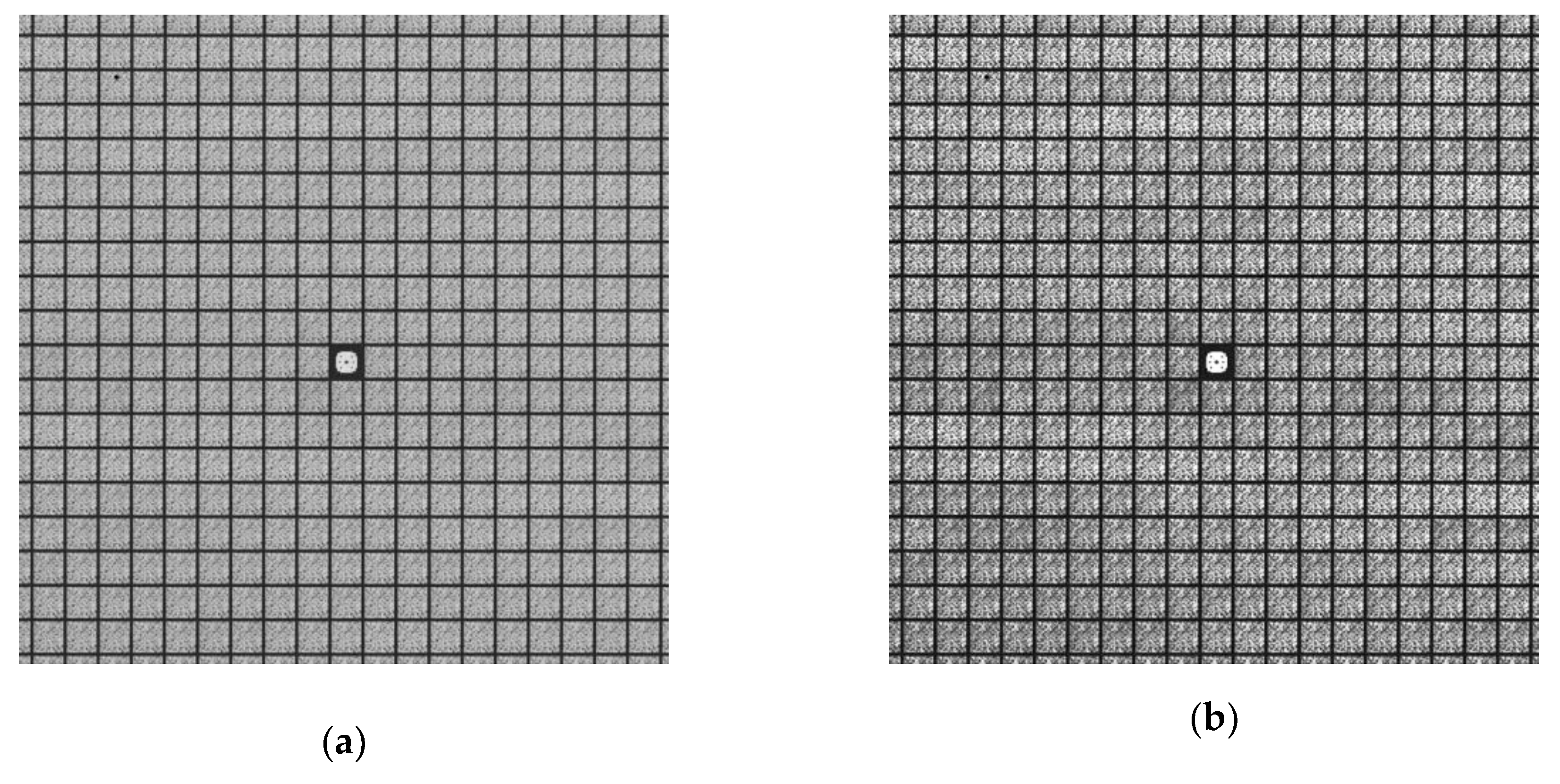
- Histogram equalization is applied to enhance the contrast on this cropped patch. Hence, for different imaging settings of the SAT, consistent performance is maintained when conducting the following steps. Figure 2 shows the results of the cropped patch before and after histogram equalization.
- An initial template with a size of is randomly cropped from the patch , as shown in Figure 3. If step 3 is skipped, we crop this initial template from the grayscale SAT image.
- An ordinary template matching process is conducted to find the parts of image that are similar to template . This step simply slides the initial template image over the patch as in a two-dimensional convolution and calculates the following metric for comparing the template against the local region of the patch .where indicates one of the pixels covered by the template for and , is the local region of patch , and is the normalized cross-correlation between two evaluated images and . Hence, the pixel forms a correlation map for and . Figure 4 shows the results of map obtained from the patches shown in Figure 2b and Figure 3. Notably, the bright pixels indicate that a high similarity occurs at these locations.
- A binary thresholding process is applied on this map to obtain a binary map as follows:This step sets the pixels that correspond with the relatively high correlation values to one and sets others to zero.
- A morphological opening operation is conducted to reduce small noise in map . Figure 5 shows the results of this step. As observed from the enlarged region depicted on the right, each presented bright dot is an object that is formed with connected bright pixels.
- The connected component method is applied to label all bright objects in map , and then calculate the centroid of every object. Here, denotes the center of the -th object, and for a total of objects obtained from .
- A set of displacement tuples is found by considering every possible pair of , for and .Here, we only count under the condition satisfying because is equal to .
- Every displacement vector contributes to a voting space as follows:Similar to the voting technique used in Hough transform, we accumulate all displacement vectors in the voting space to determine the parameters (width and height) of the template.
- Similar to steps 7–9, the centroid of every local peak is found in this voting space, and the centroid that is nearest to the origin of is then localized. Therefore, the template size is estimated as follows:
2.1.2. Standard Template Extraction
We now want to find regularly repeated regions inside the initial template (as shown in Figure 3). The process of finding such a region is described in detail as follows.
- The initial template is first smoothed using a two-dimensional Gaussian filter with a kernel size of 5 5 pixels. Because the weights are effectively zero out of a 5 5 filter when approximating to Gaussian function with a standard deviation , we select this kernel size in this study.
- After labeling all bright objects, the largest one is found and its centroid is recorded.
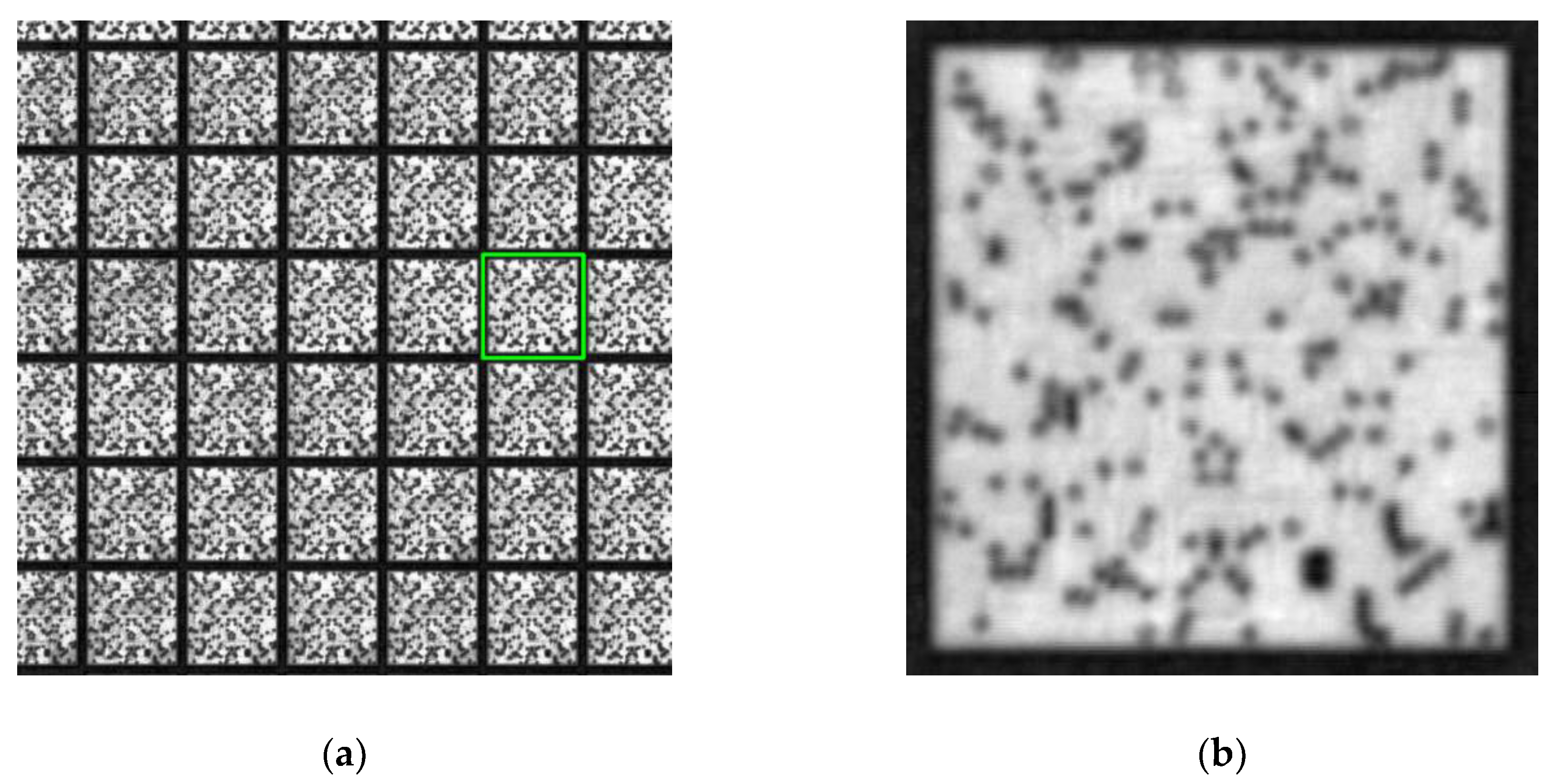
- A patch centered at is cropped to a size of pixels from the initial template. This cropped image can be considered the standard template. In Figure 7, the green rectangle in subplot (a) shows the extracted template and (b) shows its close-up.
This extracted template is used to detect the die patterns in the initial template to check whether the number of detected die patterns is sufficient. If the number of patterns is insufficient, the algorithm of automatic template extraction is re-conducted.
2.2. Die Pattern Detection and Clustering
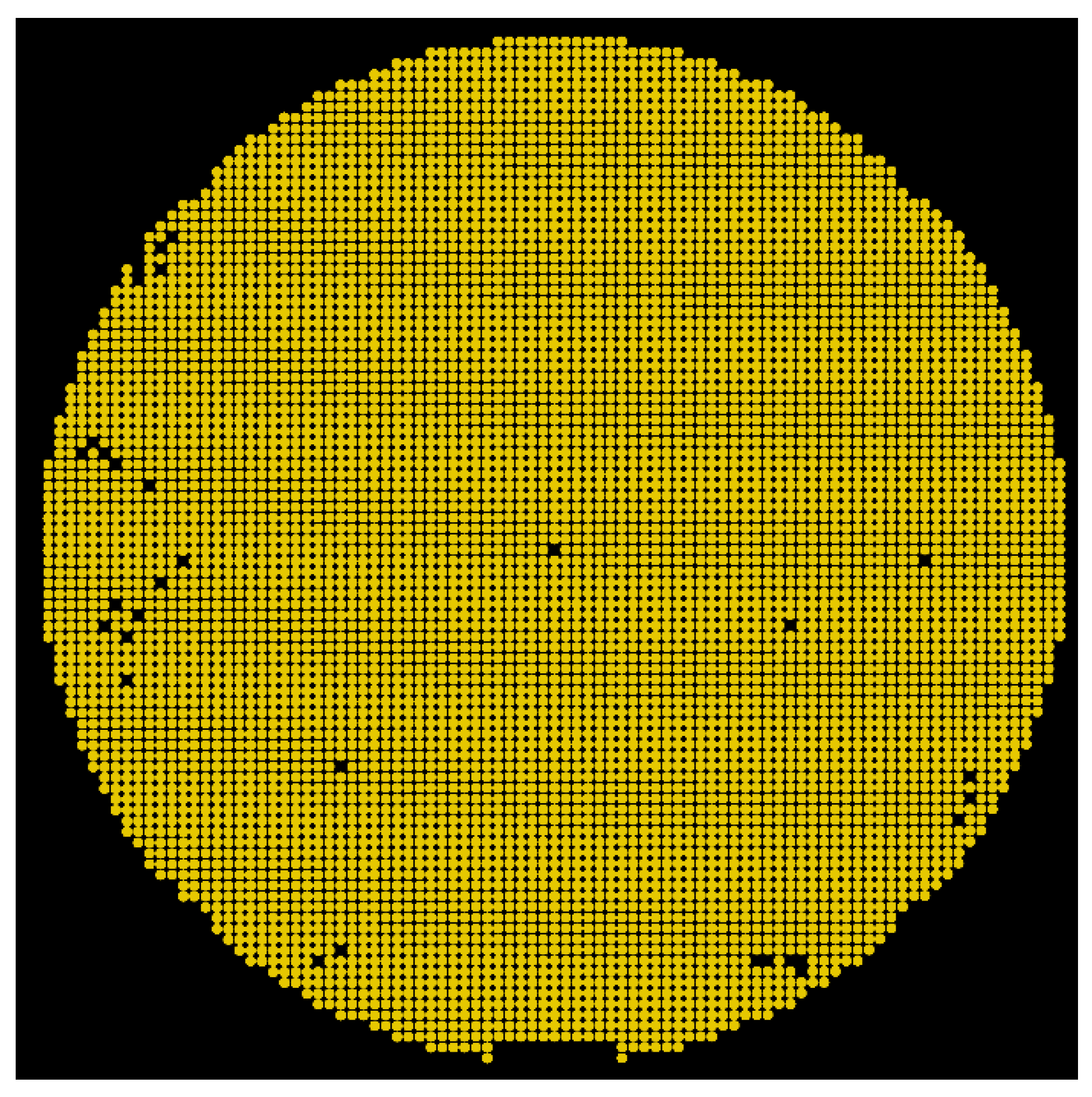
Die patterns that are similar to the standard template are expected to be detected from the original SAT image. Following steps 6–9 described in the template size estimation of Section 2.1, regions that are highly similar to the template are obtainable. The yellow dot in Figure 8 indicates that there is a die pattern found at that location, that is, a region similar to the template exists. Notably, some die patterns are not detected because their similarity is insufficiently high. They possibly result from imaging anomalies, wafer fabrication defects, and belonging to other pattern types such as alignment marks. From Figure 8, it is evident that the detected die patterns are arranged in rows and columns, and the mis-detected die patterns (dark holes inside the wafer) are possibly retrieved from their neighboring dies. Therefore, this subsection presents a clustering method for obtaining the columns and rows in the arrangement by using the detected die patterns and predicting the coordinates of these rows and columns. Eventually, the positions of these mis-detected patterns can be obtained via interpolation or extrapolation approaches.
Let be the -th detected die pattern and be its top-left corner for , where is the total number of detected patterns. In general, the wafer is well aligned during the SAT imaging process; consequently, die patterns are neatly arranged in rows and columns. The die patterns in the same column (or row) possess almost the same horizontal (or vertical) location (or ). Hence, a simple clustering method using a distance metric is used for grouping along the horizontal direction, and then find the number of columns. The criterion is to produce clusters with short intra-cluster distances and long inter-cluster distances. Let us first define a distance threshold as , the index set of which is , the selected set is empty, and the cluster set is empty. The proposed algorithm for clustering is briefly introduced as follows.
- Let the first coordinate point be taken as the first cluster center . Let the selected set be , and the cluster set .
- Select the next point from , and compute the distance for every . Apply index into set .
- Compare this distance with the threshold . If , then set belonging to cluster . Next, update center by averaging all coordinate points belonging to cluster . In contrast, let become a new prototype point, and add a new cluster with its center . Here, denotes the number of clusters in .
- Repeat steps 2–3 until all coordinate points belong to their corresponding clusters.
The four steps above form an iteration obtaining the clusters with centers. Based on these clusters, a new iteration is created to assign all coordinate points to their nearest cluster in the same manner. This clustering algorithm will terminate when the clustered results of two consecutive iterations are the same. Consequently, the number and coordinates of the columns from all detected die patterns can be obtained.
Similarly, the coordinate points are clustered in the same manner. Thus, every row and its representative coordinate are obtained. Thus far, the number of columns and rows from the detected die patterns can be obtained. Assuming that the detected patterns arrange in columns and rows. Let be the top-left corner of an arbitrary die pattern in the original SAT image, where the subscript denotes the column and subscript denotes the row. Using these corners and the estimated size of the standard template, all patterns, including the die patterns and predicted pattern candidates, in the wafer image can be obtained.
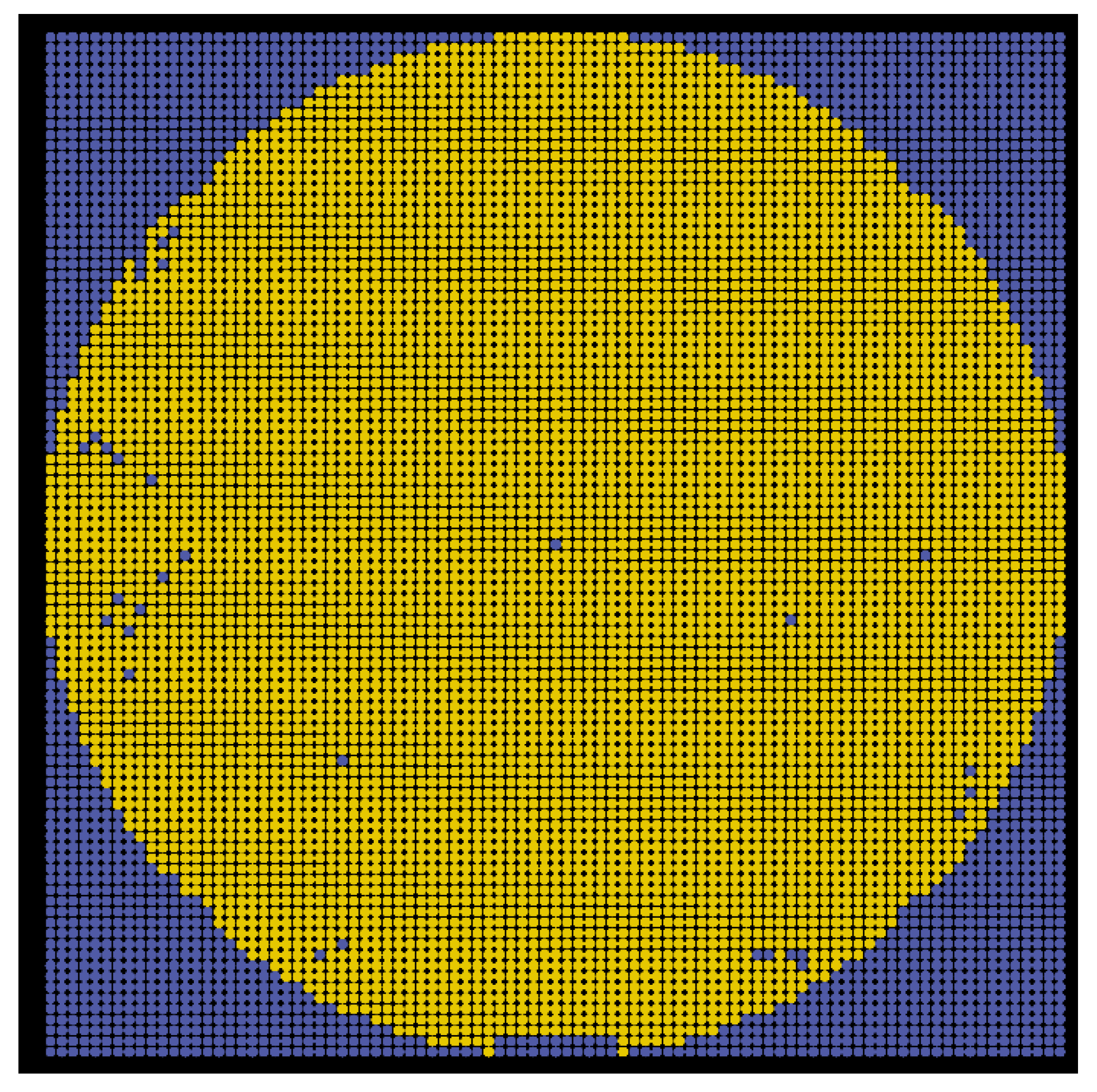
This indicates the two-dimensional region of the pattern located on the column and row. Figure 9 shows all patterns, in which the yellow and blue dots denote the locations of the detected and predicted patterns, respectively. Every pattern will be further categorized into normal, abnormal, or other predefined classes. At this point, the initial wafer map is produced; however, the patterns need to be identified later.
2.3. Pattern Classification for Inspection
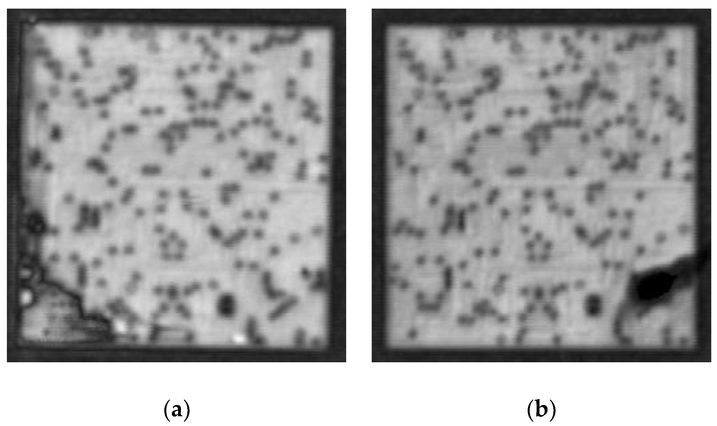
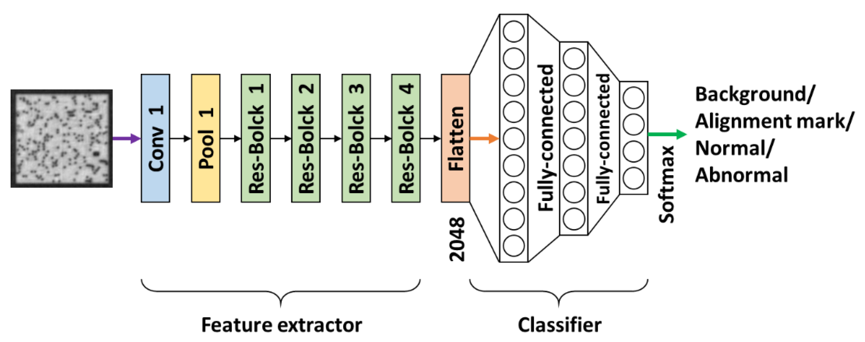
As shown in Figure 9, a wafer map full of the detected (yellow) and predicted (blue) patterns was produced. In this subsection, we further categorize each of them into one of the following classes: (1) background (outside the wafer), (2) alignment mark, (3) normal (non-defective die), or (4) abnormal (with some errors, such as cracks, defects, or imaging noise). Figure 10 shows typical examples of these four classes. In addition, more cases of different abnormal patterns are shown in Figure 11, which are caused by fabrication defects (subplots (a) to (d)), such as cracks, and imaging errors caused by voids (subplots (c) to (d)). The next task is to perform our image classification method to analyze any patterns. Here, a learning-based method composed of image feature extraction and image classification was used in our study. Numerous networks possessing a deep architecture have verified the effectiveness of the image extraction. As mentioned in Section 1, we selected several popular image feature extraction models, including VGG-16 and VGG-19 [12], InceptionV3 [16], MobileNet [18], and ResNet-50 [14], for evaluation. ResNet-50 was finally chosen as the image extractor of our proposed method. The details of the performance comparison are described in Section 3.3. This image extractor is followed by a fully-connected neural network designed for image classification. Thus, the entire architecture of our proposed method for pattern identification is as depicted in Figure 12. The details of its implementation are provided in Section 3.1.
3. Implementation and Experimental Results
First, three SAT images captured from different wafers (in the same batch) on the semiconductor production line were prepared for the following experiments. For convenience, we named them img01, img02, and img03. In this section, we focus on the explanation and implementation of (1) automatic template extraction, (2) the training and testing stages of our pattern classification method, and (3) a discussion on using different networks as the backbone of the image feature extractor. To meet the computational requirements when executing a deep CNN-based model, a graphics processing unit (GPU)-accelerated computer was used to implement our proposed method. We run all the experiments on the computer with an Intel Core I7-8750H CPU @ 2.2 GHz, 16G DDR4 RAM 2400 MHz, NVIDIA GeForce GTX-1060. The operating system was Windows 10. The entire algorithm was programmed in Python and used OpenCV and TensorFlow.
3.1. Experiments on Automatic Template Extraction and Die Detection
The proposed method for template extraction was verified using images img01, img02, and img03. The parameters used in this experiment are as follows:
- The size of the original SAT image is: and .
- The size of the image patch is: and . This size is determined to ensure that there are sufficient die patterns in this image patch. If template extraction fails, this size can be increased by , , and so on.
- The size of the initial template is: and . The criterion for determining this size is to ensure that there exists one (or more) whole die pattern in this initial template. Generally, this size is big enough to detect and extract a standard template.
- The similarity threshold is the 90th percentile value of the map , that is, .
- The binarization thresholds are adaptively determined using Otsu’s method [20].
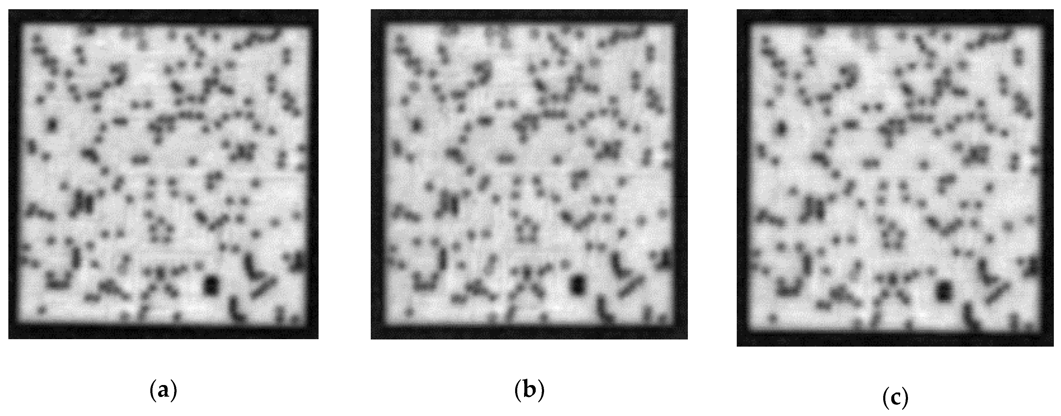
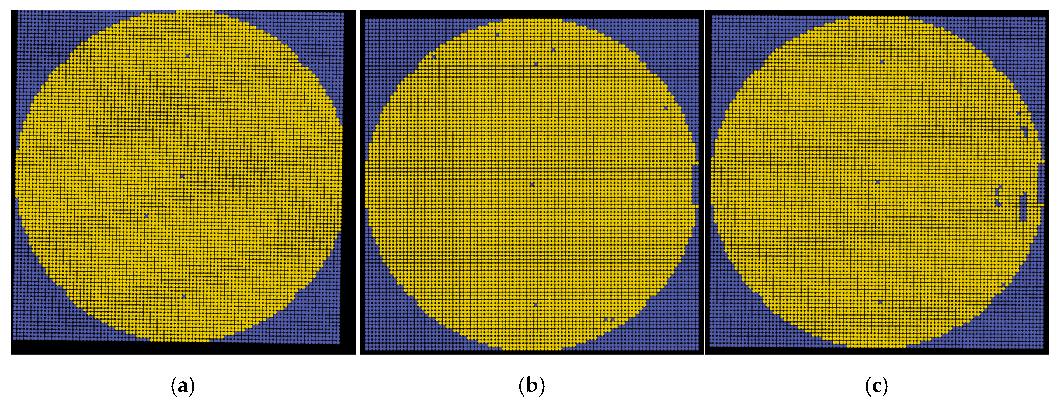
Figure 13 shows the extracted templates, in which subplots (a), (b), and (c) correspond to img01, img02, and img03, respectively, and the estimated template size can be found in Table 1. These are very similar because their original SAT images are from the same batch of wafer products. Next, we apply template matching followed by clustering to obtain an initial wafer map that contains the detected die patterns (marked by the yellow dots) and predicted pattern candidates (marked by the blue dots). Figure 14 shows the results of the initial wafer maps for images img01, img02, and img03. These wafer maps need to be further analyzed by conducting our proposed classification model for every pattern.
3.2. Implementation of Die Pattern Classification
In this subsection, the proposed pattern classification model trained using our own dataset is described. The standard network, as depicted in Figure 12, contains over 25 million trainable parameters. The first half of the network is a ResNet-50 feature extractor, the input of which is a normalized pattern image with a size of 224 224 pixels and a feature vector output of 2048 1. The complete compositions of ResNet-50 are shown in Table 2. The second half is a fully-connected neural network applied to conduct four-class classification, the thorough architecture of which is tabulated in Table 3.
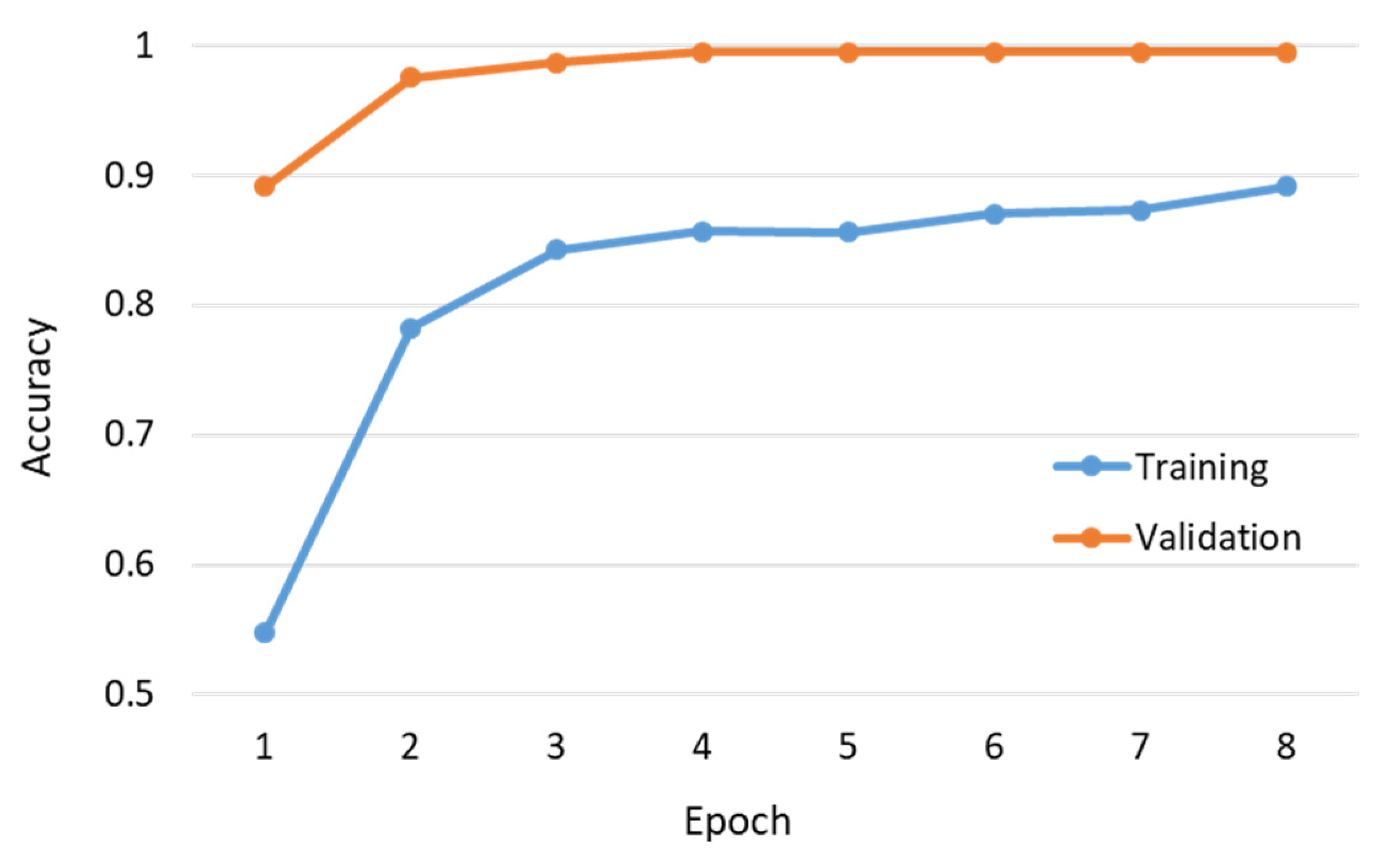
During this experiment, we collected a total of 2150 samples to form our own Dataset-I, and manually identified them into four categories: (1) background, (2) alignment mark, (3) normal, and (4) abnormal. Repeated random subsampling validation [21], also known as Monte Carlo cross-validation, was adopted for evaluating accuracy during training. The Dataset-I was randomly split into training and validation sets multiple times, whereas the ratio of training data to validation data was 5:1. For each such split, the model was learned with the training set, and the accuracy was assessed using the validation set. The accuracies obtained from the splits were then averaged. Table 4 lists the data distribution of which were 1769 samples used for learning the model and 381 samples applied for validation. Some commonly used data augmentation techniques are applied in the present work, including shifting and flipping, rotation, and brightness shifts. We set the hyper-parameters as follows: rotation range of , spatial shifts of , brightness shifts of , a random zoom range of , dropout probability of , batch size of 8, maximum epochs of 15, optimized using Adam with commonly-used settings of , , and , and the learning rate of . Figure 15 shows the per-epoch trend of training and validation accuracy. Note that we terminated the training process after eight epochs because the training and validation accuracy converged to 89.13% and 99.46%, respectively. As shown in the figure, the training accuracy is less than the validation accuracy; this situation can be attributed to several reasons: (1) the regularization mechanisms, such as the dropout and L1/L2 weight regularization, were turned on during training. (2) When using the Keras library in the TensorFlow, the training accuracy for an epoch is the averaged accuracy over each batch of the training data. Because the model was changing over time, the accuracy over the first batch was lower than that over the last batch. By contrast, the validation accuracy for an epoch is computed using the model as it is at the end of the epoch, resulting in a higher accuracy. (3) The techniques of data augmentation used during training probably produced certain samples that were difficult to identify. Finally, we used 370 additional test data for evaluating the learned model, the results of which are summarized in Table 5 as a confusion matrix. Notably, the test data were collected from different batches of wafers. Only two normal samples were incorrectly identified as an abnormal class. The overall accuracy was greater than 99%, and the accuracy for the normal samples was 98.57%.
3.3. Comparison among Feature Extractors
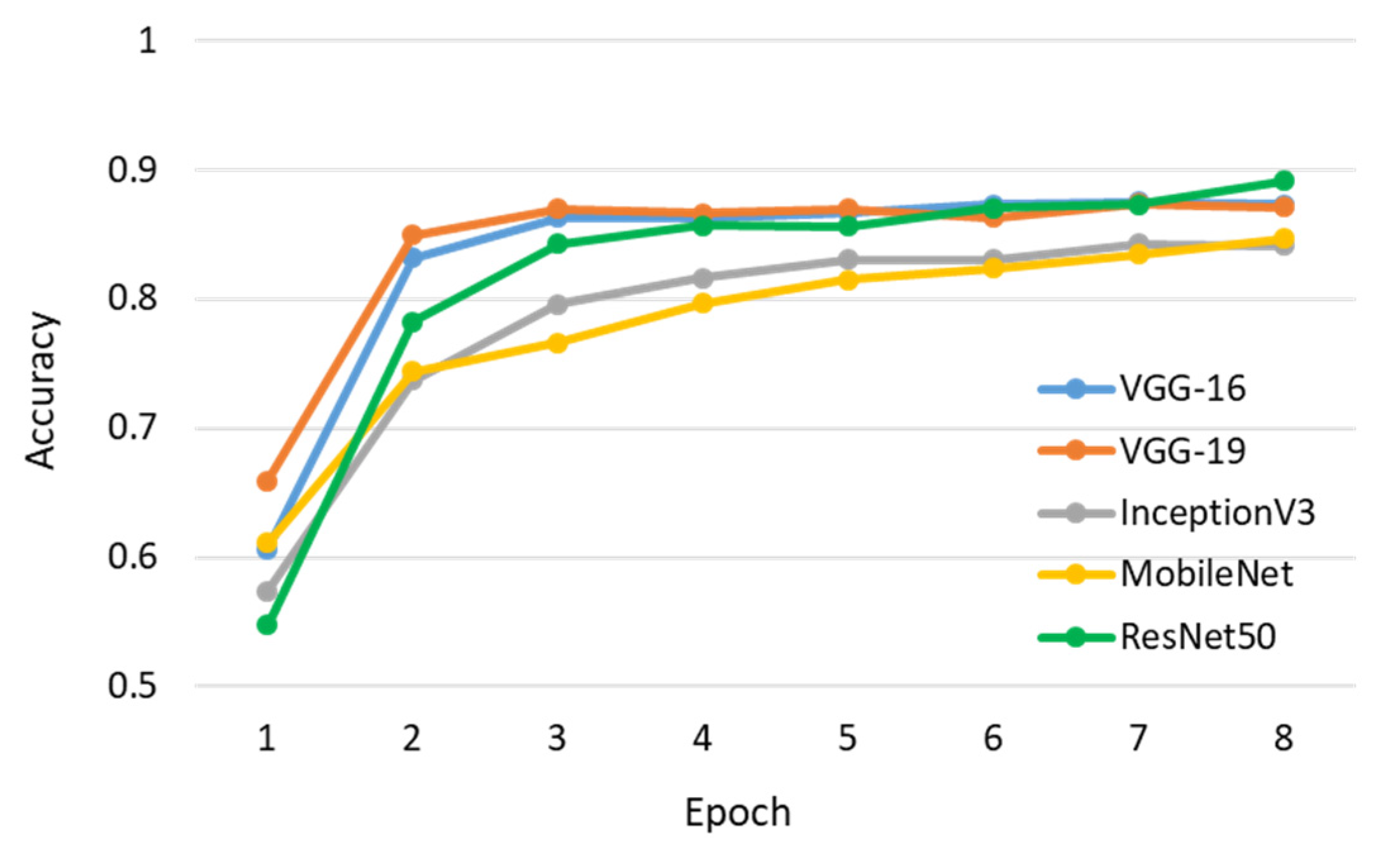
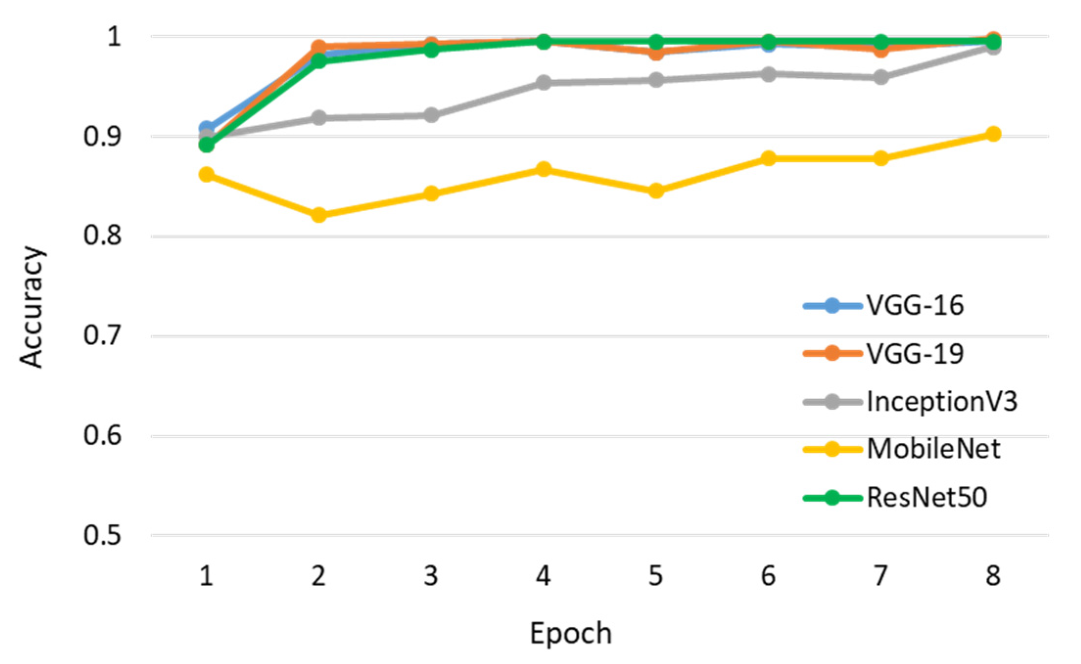
When designing the architecture of our deep model, several CNN-based models that are frequently used in image featuring were evaluated. In this subsection, five popular backbones, namely, VGG-16 and VGG-19 [12], InceptionV3 [16], MobileNet [18], and ResNet-50 [14], were chosen for comparison. For fairness, their inputs were normalized to an identical size and followed by the same classifier. Their training and validation accuracy are presented separately in Figure 16 and Figure 17. Notably, the training and validation accuracy were relatively high in the early epoch because these compared backbones were pre-trained on the ImageNet dataset [22]. It can be seen that ResNet-50 outperformed other approaches after six epochs, whereas VGG-16 and VGG-19 showed comparable accuracy. Moreover, a computational comparison between these backbones is listed in Table 6. Here, the minimum, maximum, and average computational time for identifying a pattern image and the total number of parameters of different models are also summarized. The VGG-16 and VGG-19, whose accuracies were comparable to ResNet-50, have a much larger number of model parameters. To consider the balance between accuracy and computational time, ResNet-50 was chosen as the standard subnetwork for the image feature extractor applied in our proposed method. More discussion on different CNN-based networks is provided in Section 4.1.
3.4. Wafer Map Generation for Inspection Visualization
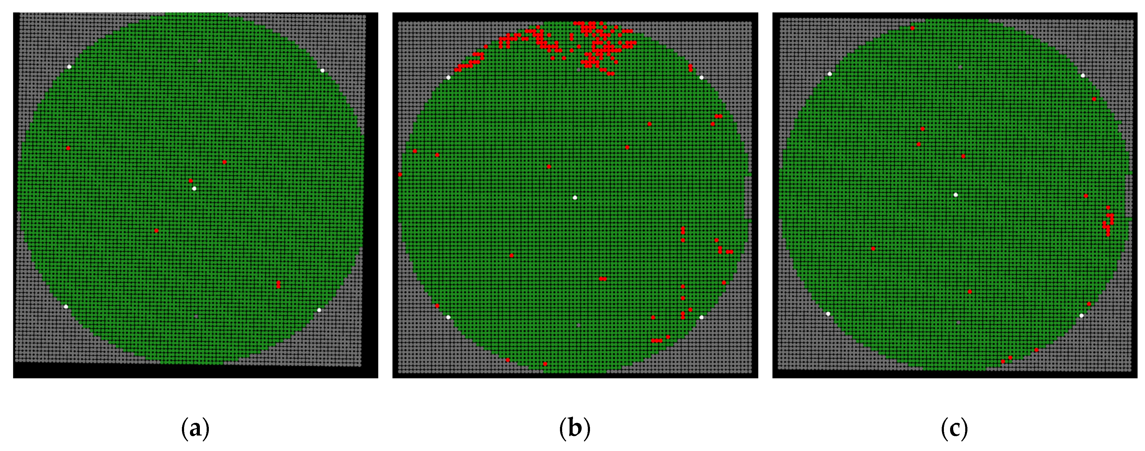
The final result of our proposed method is a multi-class wafer map, the classes of which can be manually defined by users. In this paper, four classes are applied: background, alignment mark, and normal and abnormal patterns. Let the original SAT image be the input; thereafter, automatic template extraction, pattern detection, and prediction steps, followed by pattern classification, are conducted. All patterns are found, and the information of each pattern, including the location, width, height, and its class is also obtained. Figure 18 shows the final results corresponding to images img01, img02, and img03. The patterns belonging to the background, alignment mark, and normal and abnormal pattern classes are plotted in gray, white, green, and red, respectively. The analyzed wafer maps are useful for visualizing defects and finding potential fabrication issues.
4. Discussion
4.1. More Discussion on Pattern Classification Models
The implementation and experimental evaluation of our proposed method have been described in Section 3. The deep learning-based pattern classification model was designed to consist of a ResNet-50-based extractor and a multi-layer fully-connected classifier. The rationale for determining the extractor and the hyper-parameters of the classifier was attaining high accuracy and less computational time. To analyze the accuracies of different model structures, we collected a total of 10,180 samples that were captured from four batches of wafers to form Dataset-II of which contained: (1) 2008 background patterns, (2) 408 alignment mark patterns, (3) 6184 normal patterns, and (4) 1580 abnormal patterns. Similarly, the random subsampling validation was repeated multiple times to assess each of the classification models. Table 7 lists the size of the feature vector obtained by a specified extractor and the total number of parameters of a model with a specified composition of hidden layers. In this table, the tuple (1000) denotes that the classifier contains one hidden layer with 1000 neurons, and the tuples (1000, 100) and (1000, 100, 10) respectively indicate two and three hidden layers with their neurons. It is evident that the ResNet-50 generated the most compact feature vector (having the minimum size) and thus structured the smallest classification model. Table 8 lists the validation accuracy of Dataset-II for the aforementioned compositions. The results showed that VGG-16, VGG-19, and ResNet-50 achieved comparatively high accuracy. For every extractor, the best accuracy was obtained when the classifier comprised two hidden layers. To sum up, the architecture consisting of a ResNet-50 extractor and a two-hidden-layer classifier was selected for our proposed classification model. Subsequently, a grid search approach was used to find the number of neurons in each of the hidden layers. During this experiment, we evaluated several combinations for two-hidden-layer composition , where and were respectively selected from and . The results were tabulated in Table 9, in which the accuracies were close to each other. However, the two-layer composition has unlimited possible combinations, and cannot be completely assessed; thus, the composition (1000, 100) that reached a high accuracy is an acceptable hyper-parameter setting in the model. In this subsection, the experimental results in terms of accuracy and computation time are consistent with [23]. The ResNet-50 indeed has a more efficient accuracy density (accuracy per parameter) than VGG-16 and VGG-19 networks.
4.2. Generalizing to Inspect More Abnormal Patterns
As mentioned, our proposed wafer inspection method can identify four categories of patterns, including the background, alignment mark, normal, and abnormal classes. This method is practical for identifying more than four classes by modifying the output layer of the classifier. In this subsection, a classification model that can determine the background, alignment mark, normal pattern, imaging error, crack, and pinhole verified the feasibility of inspecting such defective patterns. Similar to the experimental procedure conducted in Section 3, we used Dataset-I for training and the same 370 test data for evaluating the accuracy. Table 10 summarizes the results as a confusion matrix, in which there were a total of 17 data incorrectly identified. Such increased errors are often caused by imbalanced data distribution in the Dataset-I of which the crack and pinhole samples were far fewer than others, even though data augmentation techniques were applied during training. In general wafer inspection applications, all the defective (abnormal) die patterns need to be filtered out. Therefore, these anomaly patterns are merged into an abnormal class in the present work.
5. Conclusions
In this study, we proposed a vision-based method for detecting and recognizing dies on a wafer. The main contributions of our method include an automatic scheme of standard template extraction, clustering based on the distance to produce a wafer map, and a deep learning-based pattern classification model. Ordinary template matching was employed to detect regularly repeated die patterns. Thus, we proposed a template extraction algorithm that provides a reliable template for finding such patterns. Furthermore, a clustering technique applying the distance criterion was introduced to predict the locations of the pattern candidates. For the pattern classification phase, we designed a deep CNN-based model composed of an image feature extractor and a classifier to identify patterns as different classes. The effectiveness and efficiency of our proposed method were evaluated experimentally. Furthermore, qualitative and quantitative evaluations were also conducted. By applying the proposed visual inspection method, SAT images from wafers can be analyzed completely and used to form wafer maps. These wafer maps can provide important information for finding and analyzing wafer manufacturing problems in the semiconductor industry.
Funding
This research was supported in part by National United University under the Grant 1081020.
Conflicts of Interest
The author declares there are no conflicts of interest regarding the publication of this paper.
References
- Huang, S.H.; Pan, Y.C. Automated visual inspection in the semiconductor industry: A survey. Comput. Ind. 2015, 66, 1–10. [Google Scholar] [CrossRef]
- Shankar, N.G.; Zhong, Z.W. Defect detection on semiconductor wafer surfaces. Microelectron. Eng. 2005, 77, 337–346. [Google Scholar] [CrossRef]
- Schulze, M.A.; Hunt, M.A.; Voelkl, E.; Hickson, J.D.; Usry, W.; Smith, R.G.; Bryant, R.; Thomas, C.E., Jr. Semiconductor wafer defect detection using digital holography. In Proceedings of the SPIE 5041, Process and Materials Characterization and Diagnostics in IC Manufacturing, Santa Clara, CA, USA, 27–28 Febuary 2003; pp. 183–193. [Google Scholar]
- Kim, S.; Oh, I.S. Automatic defect detection from SEM images of wafers using component tree. J. Semicond. Tech. Sci. 2017, 17, 86–93. [Google Scholar] [CrossRef]
- Yeh, C.H.; Wu, F.C.; Ji, W.L.; Huang, C.Y. A wavelet-based approach in detecting visual defects on semiconductor wafer dies. IEEE Trans. Semicond. Manuf. 2010, 23, 284–292. [Google Scholar] [CrossRef]
- Pan, Z.; Chen, L.; Li, W.; Zhang, G.; Wu, P. A novel defect inspection method for semiconductor wafer based on magneto-optic imaging. J. Low Temp. Phys. 2013, 170, 436–441. [Google Scholar] [CrossRef]
- Hartfield, C.D.; Moore, T.M. Acoustic Microscopy of Semiconductor Packages. In Microelectronics Failure Analysis: Desk Reference, 6th ed.; Ross, R.J., Ed.; ASM International: Materials Park, OH, USA, 2011; pp. 362–382. [Google Scholar]
- Sakai, K.; Kikuchi, O.; Kitami, K.; Umeda, M.; Ohno, S. Defect detection method using statistical image processing of scanning acoustic tomography. In Proceedings of the IEEE 23rd International Symposium on the Physical and Failure Analysis of Integrated Circuits, Singapore, 18–21 July 2016; pp. 293–296. [Google Scholar]
- Kitami, K.; Takada, M.; Kikuchi, O.; Ohno, S. Development of high resolution scanning aeoustie tomograph for advanced LSI packages. In Proceedings of the IEEE 20th International Symposium on the Physical and Failure Analysis of Integrated Circuits, Suzhou, China, 15–19 July 2013; pp. 522–525. [Google Scholar]
- Sakai, K.; Kikuchi, O.; Takada, M.; Sugaya, N.; Ohno, S. Image improvement using image processing for scanning acoustic tomograph images. In Proceedings of the IEEE 22nd International Symposium on the Physical and Failure Analysis of Integrated Circuits, Hsinchu, Taiwan, 29 June–2 July 2015; pp. 163–166. [Google Scholar]
- Brunelli, R. Template Matching as Testing. In Template Matching Techniques in Computer Vision: Theory and Practice, 1st ed.; John Wiley & Sons Ltd.: West Sussex, UK; New York, NY, USA, 2009; pp. 43–71. [Google Scholar]
- Simonyan, K.; Zisserman, A. Very deep convolutional networks for large-scale image recognition. arXiv 2014, arXiv:1409.1556. [Google Scholar]
- Krizhevsky, A.; Sutskever, I.; Hinton, G.E. Imagenet classification with deep convolutional neural networks. In Proceedings of the Advances in Neural Information Processing Systems 2012, Lake Tahoe, CA, USA, 3–8 December 2012; pp. 1097–1105. [Google Scholar]
- He, K.; Zhang, X.; Ren, S.; Sun, J. Deep residual learning for image recognition. In Proceedings of the IEEE Conference on Computer Vision and Pattern Recognition 2016, Las Vegas, NV, USA, 26 June–1 July 2016; pp. 770–778. [Google Scholar]
- Szegedy, C.; Liu, W.; Jia, Y.; Sermanet, P.; Reed, S.; Anguelov, D.; Erhan, D.; Vanhoucke, V.; Rabinovich, A. Going deeper with convolutions. In Proceedings of the IEEE Conference on Computer Vision and Pattern Recognition 2015, Boston, MA, USA, 7–12 June 2015; pp. 1–9. [Google Scholar]
- Szegedy, C.; Vanhoucke, V.; Ioffe, S.; Shlens, J.; Wojna, Z. Rethinking the inception architecture for computer vision. In Proceedings of the IEEE Conference on Computer Vision and Pattern Recognition 2016, Las Vegas, NV, USA, 26 June–1 July 2016; pp. 2818–2826. [Google Scholar]
- Szegedy, C.; Ioffe, S.; Vanhoucke, V.; Alemi, A.A. Inception-v4, inception-resnet and the impact of residual connections on learning. In Proceedings of the Thirty-First AAAI Conference on Artificial Intelligence, San Francisco, CA, USA, 4–10 Febuary 2017; pp. 4278–4284. [Google Scholar]
- Howard, A.G.; Zhu, M.; Chen, B.; Kalenichenko, D.; Wang, W.; Weyand, T.; Andreetto, M.; Adam, H. Efficient convolutional neural networks for mobile vision applications. arXiv 2017, arXiv:1704.0486. [Google Scholar]
- Nakazawa, T.; Kulkarni, D.V. Wafer map defect pattern classification and image retrieval using convolutional neural network. IEEE Trans. Semicond. Manuf. 2018, 31, 309–314. [Google Scholar] [CrossRef]
- Sezgin, M.; Sankur, B. Survey over image thresholding techniques and quantitative performance evaluation. J. Electron. Imaging 2004, 1, 146–166. [Google Scholar] [CrossRef]
- Picard, R.R.; Cook, R.D. Cross-validation of regression model. J. Am. Stat. Assoc. 1984, 79, 575–583. [Google Scholar] [CrossRef]
- Russakovsky, O.; Deng, J.; Su, H.; Krause, J.; Satheesh, S.; Ma, S.; Huang, Z.; Karpathy, A.; Khosla, A.; Bernstein, M.; et al. ImageNet large scale visual recognition challenge. Int. J. Comput. Vis. 2015, 115, 211–252. [Google Scholar] [CrossRef] [Green Version]
- Bianco, S.; Cadene, R.; Celona, L.; Napoletano, P. Benchmark analysis of representative deep neural network architectures. IEEE Access 2018, 6, 64270–64277. [Google Scholar] [CrossRef]
Figure 1.
Original scanning acoustic tomography (SAT) image: example wafer.
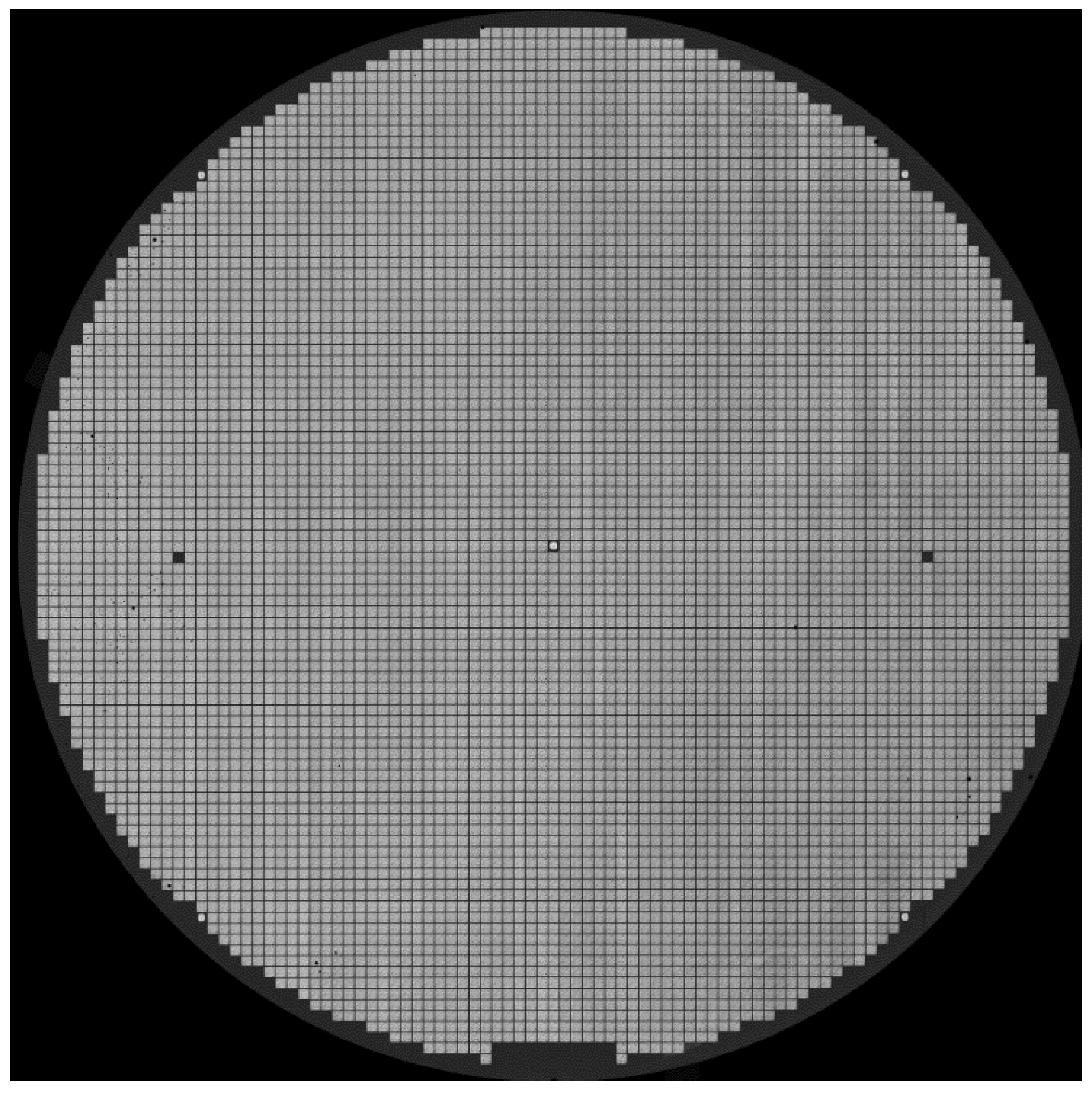
Figure 2.
Cropped patch from Figure 1: (a) before and (b) after histogram equalization.
Figure 2.
Cropped patch from Figure 1: (a) before and (b) after histogram equalization.

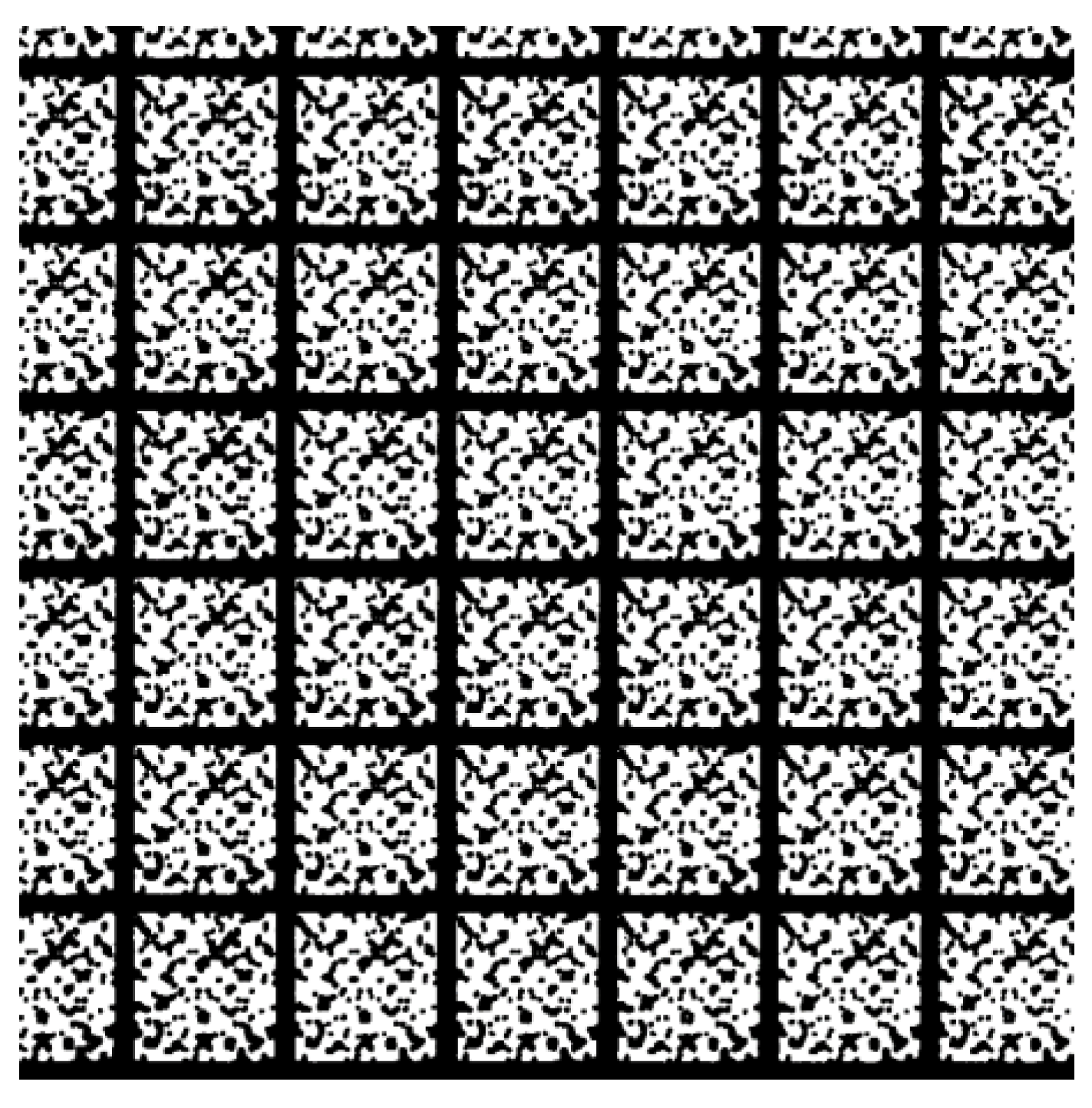
Figure 3.
Initial template.
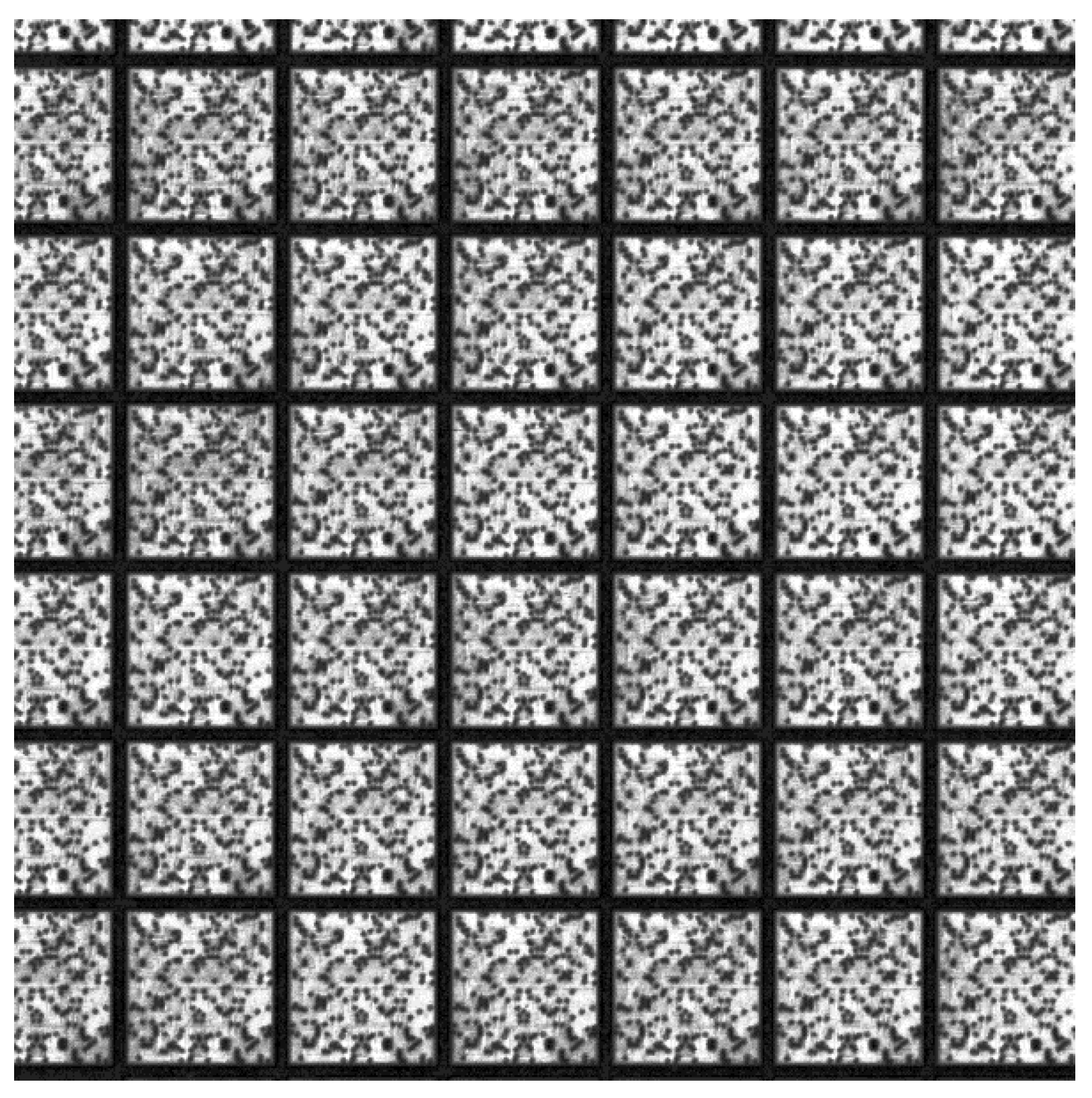
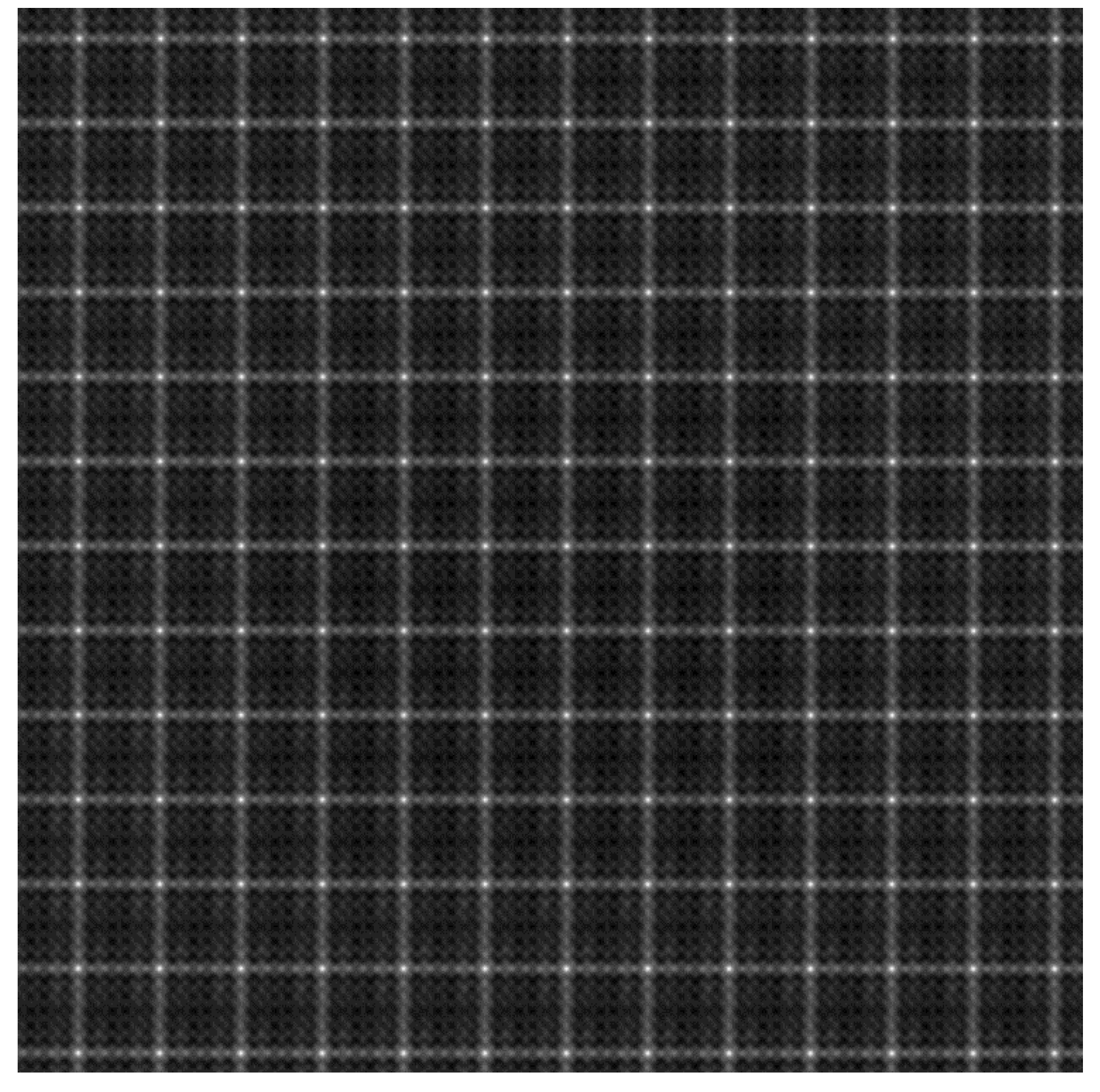
Figure 5.
Results of binary-thresholding followed by the opening from the correlation map.
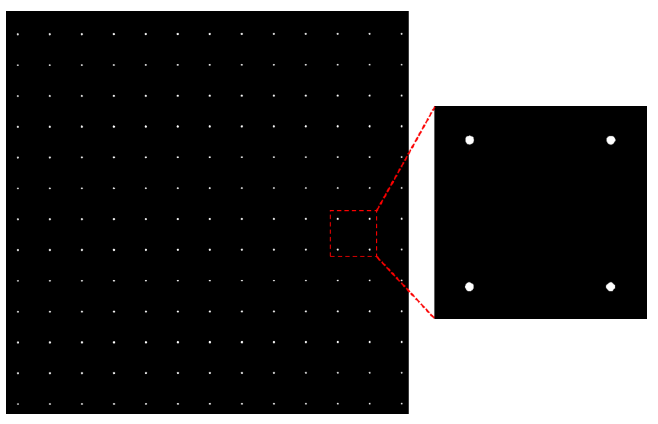
Figure 6.
Binarized image of the initial template in Figure 3.
Figure 6.
Binarized image of the initial template in Figure 3.

Figure 7.
Patches: (a) extracted from the initial template; (b) used as a standard template.

Figure 8.
Die detection result of original SAT image.

Figure 9.
Initial wafer mapping result from detected and predicted die patterns.

Figure 10.
Four different patterns: (a) background; (b) alignment mark; (c) normal; (d) abnormal pattern.
Figure 10.
Four different patterns: (a) background; (b) alignment mark; (c) normal; (d) abnormal pattern.
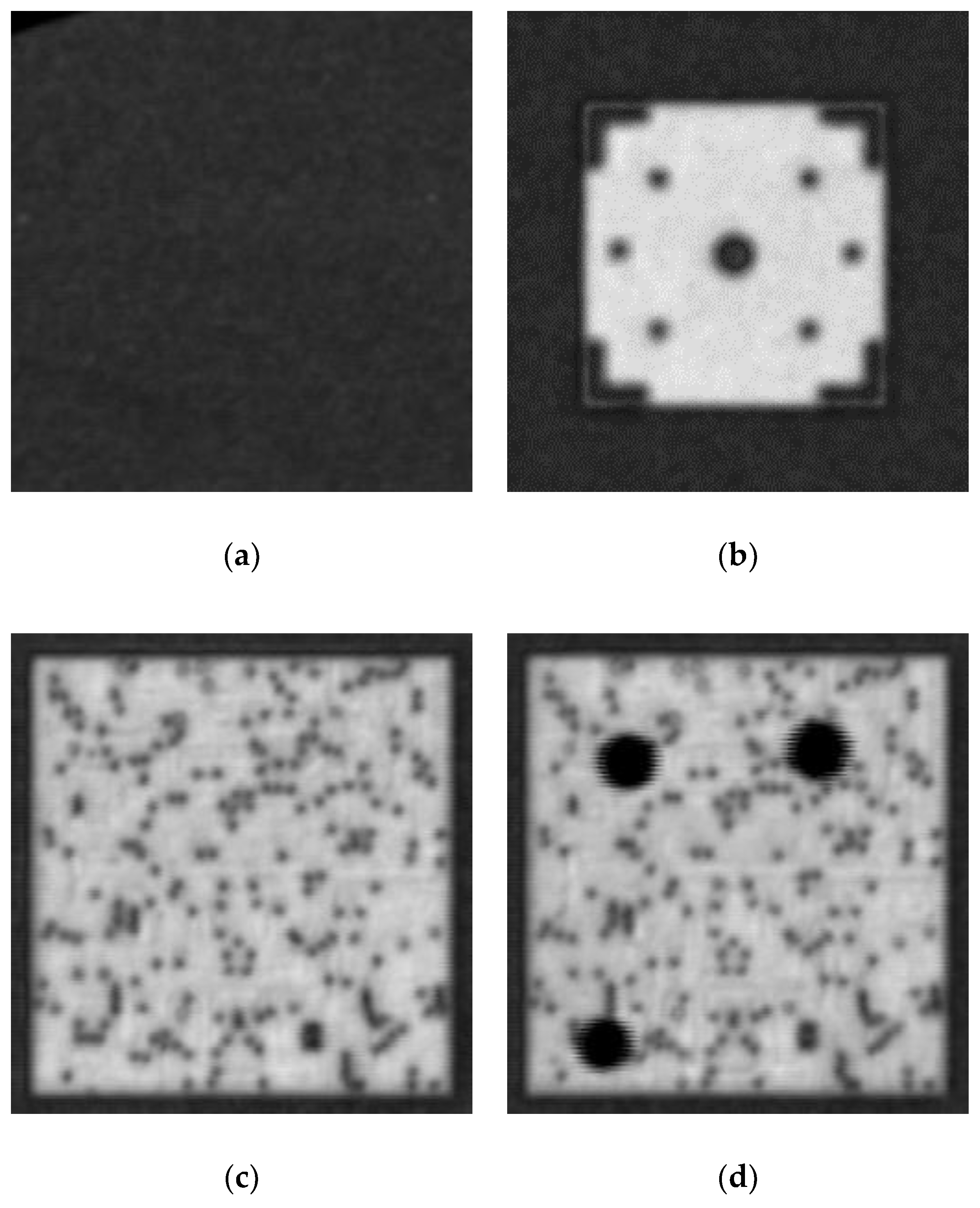
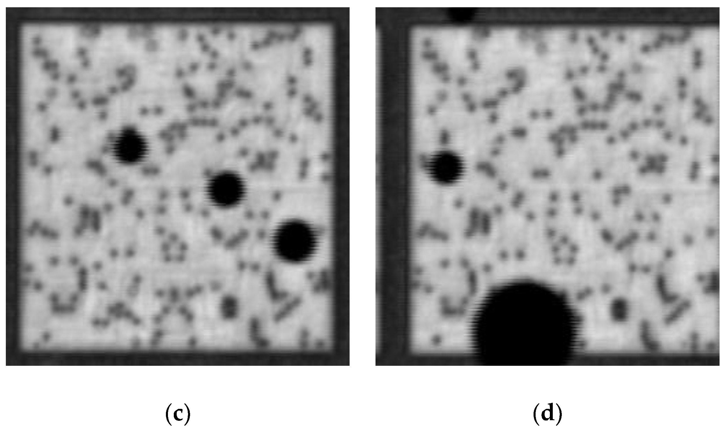
Figure 11.
More examples of abnormal patterns: (a) crack; (b) defect; (c) and (d) errors caused by voids.
Figure 11.
More examples of abnormal patterns: (a) crack; (b) defect; (c) and (d) errors caused by voids.


Figure 12.
Deep convolutional neural network (CNN) for die pattern classification.

Figure 13.
Results of template extraction for three SAT images: (a) img01; (b) img02; (c) img03.

Figure 14.
Results of die pattern detection for three SAT images: (a) img01; (b) img02; (c) img03.

Figure 15.
Training and validation accuracy.

Figure 16.
Training accuracy for different CNN-based networks.

Figure 17.
Validation accuracy for different CNN-based networks.

Figure 18.
Results of our proposed inspection method for three SAT images: (a) img01; (b) img02; (c) img03.
Figure 18.
Results of our proposed inspection method for three SAT images: (a) img01; (b) img02; (c) img03.

Table 1.
Numerical results of die pattern detection.
| Image | Template | Template Size (Unit: Pixels) | # of Detected Die Patterns | # of Predicted Regions |
|---|---|---|---|---|
| img01 | 13(a) | 6745 | 1718 | |
| img02 | 13(b) | 6756 | 1889 | |
| img03 | 13(c) | 6763 | 1882 |
Table 2.
Architecture of feature extractor in our pattern classification model.
| Feature Extractor: ResNet-50 Encoder | ||||
|---|---|---|---|---|
| Layer Name | Kernel Size | Stride | Channels | Repeat Times |
| Conv 1 | 2 | 364 | 1 | |
| Pool 1 | 2 | 1 | ||
| Resblock 1 | 1 | 64256 | 3 | |
| Resblock 2 | 1 | 256512 | 4 | |
| Resblock 3 | 1 | 5121024 | 6 | |
| Resblock 4 | 1 | 10242048 | 3 | |
Table 3.
Architecture of fully connected network in our pattern classification model.
| Classifier: Fully-Connected Neural Network | ||
|---|---|---|
| Layer Name | Input Dimension | Output Dimension |
| FC-1 1 | 2048 | 1000 |
| FC-2 1 | 1000 | 100 |
| FC-3 1 | 100 | 4 |
| Softmax 2 | 4 | 4 |
1 FC = fully connected layer. 2 Softmax is used to map the output of a neural network to a probability distribution over the predicted output classes. This ensures that the sum of all output elements equals 1.
Table 4.
Data distribution in Dataset-I.
| Class Label | of Training Samples | of Validation Samples |
|---|---|---|
| Background | 417 | 83 |
| Alignment mark | 375 | 75 |
| Normal | 560 | 140 |
| Abnormal | 417 | 83 |
Table 5.
Confusion matrix for additional 370 test data.
| Predicted | Background | Alignment Mark | Normal | Abnormal | Accuracy (%) | |
|---|---|---|---|---|---|---|
| True | ||||||
| Background | 83 | 0 | 0 | 0 | 100 | |
| Alignment mark | 0 | 64 | 0 | 0 | 100 | |
| Normal | 0 | 0 | 138 | 2 | 98.57 | |
| Abnormal | 0 | 0 | 0 | 83 | 100 | |
Table 6.
Comparison of different models for pattern classification.
| Extractor | Time (Unit: ms) | Number of Extractor Parameters | Total Number of Model Parameters | ||
|---|---|---|---|---|---|
| Min. | Max. | Avg. | |||
| VGG-16 | 30.25 | 35.63 | 31.02 | 14,714,688 | 39,904,192 |
| VGG-19 | 36.75 | 39.63 | 37.19 | 20,024,384 | 45,213,888 |
| InceptionV3 | 33.38 | 45.88 | 35.02 | 21,802,784 | 73,104,288 |
| MobileNet | 24 | 30.63 | 25.03 | 3,228,864 | 53,506,368 |
| ResNet-50 | 31 | 42 | 32.58 | 23,587,712 | 25,737,216 |
Table 7.
The total number of parameters of different model structures.
| Extractor | Size of Feature Vector | Composition of Hidden Layers | ||
|---|---|---|---|---|
| (1000) | (1000, 100) | (1000, 100, 10) | ||
| VGG-16 | 25,088 | 39,807,692 | 39,904,192 | 39,904,842 |
| VGG-19 | 25,088 | 45,117,388 | 45,213,888 | 45,214,538 |
| InceptionV3 | 51,200 | 73,007,788 | 73,104,288 | 73,104,938 |
| MobileNet | 50,176 | 53,409,868 | 53,506,368 | 53,507,018 |
| ResNet-50 | 2048 | 25,640,716 | 25,737,216 | 25,737,866 |
Table 8.
Validation accuracy of different model structures.
| Extractor | Composition of Hidden Layers | ||
|---|---|---|---|
| (1000) | (1000, 100) | (1000, 100, 10) | |
| VGG-16 | 0.8701 | 0.8809 | 0.8167 |
| VGG-19 | 0.8766 | 0.8802 | 0.8673 |
| InceptionV3 | 0.8016 | 0.8206 | 0.7976 |
| MobileNet | 0.7972 | 0.8109 | 0.6548 |
| ResNet-50 | 0.8794 | 0.8817 | 0.8663 |
Table 9.
Validation accuracy of different two-layer compositions, using a ResNet-50 extractor.
| Layer 1 | Number of Neurons | |||
|---|---|---|---|---|
| Layer 2 | 1000 | 500 | 200 | |
| Number of neurons | 200 | 0.8715 | 0.8728 | 0.8756 |
| 100 | 0.8817 | 0.8789 | 0.8635 | |
| 50 | 0.8722 | 0.8810 | 0.8744 | |
Table 10.
Confusion matrix for additional 370 test data: six-class classification model.
| True | Background | Alignment Mark | Normal | Imaging Error | Crack | Pinhole | Accuracy (%) | |
|---|---|---|---|---|---|---|---|---|
| Predicted | ||||||||
| Background | 83 | 0 | 0 | 0 | 0 | 0 | 100 | |
| Alignment mark | 0 | 64 | 0 | 0 | 0 | 0 | 100 | |
| Normal | 0 | 0 | 125 | 6 | 4 | 0 | 92.59 | |
| Imaging error | 0 | 0 | 5 | 57 | 0 | 0 | 91.94 | |
| Crack | 0 | 0 | 1 | 0 | 8 | 0 | 88.89 | |
| Pinhole | 0 | 0 | 0 | 1 | 0 | 16 | 94.12 | |
© 2020 by the author. Licensee MDPI, Basel, Switzerland. This article is an open access article distributed under the terms and conditions of the Creative Commons Attribution (CC BY) license (http://creativecommons.org/licenses/by/4.0/).
Share and Cite
MDPI and ACS Style
Chen, H.-C. Automated Detection and Classification of Defective and Abnormal Dies in Wafer Images. Appl. Sci. 2020, 10, 3423. https://doi.org/10.3390/app10103423
AMA Style
Chen H-C. Automated Detection and Classification of Defective and Abnormal Dies in Wafer Images. Applied Sciences. 2020; 10(10):3423. https://doi.org/10.3390/app10103423
Chicago/Turabian StyleChen, Hsiang-Chieh. 2020. "Automated Detection and Classification of Defective and Abnormal Dies in Wafer Images" Applied Sciences 10, no. 10: 3423. https://doi.org/10.3390/app10103423
Note that from the first issue of 2016, this journal uses article numbers instead of page numbers. See further details here.