
The Effect of Current Supply Duration during Stepwise Electrical Sintering of Silver Nanoparticles

 , , and
Abstract
:1. Introduction
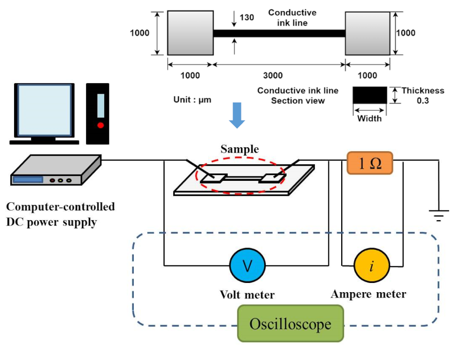
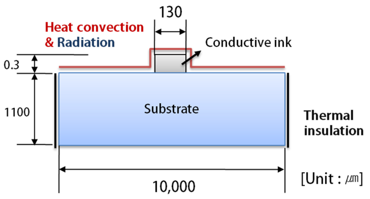
2. Materials and Method
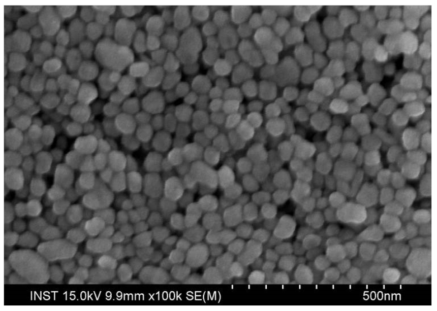
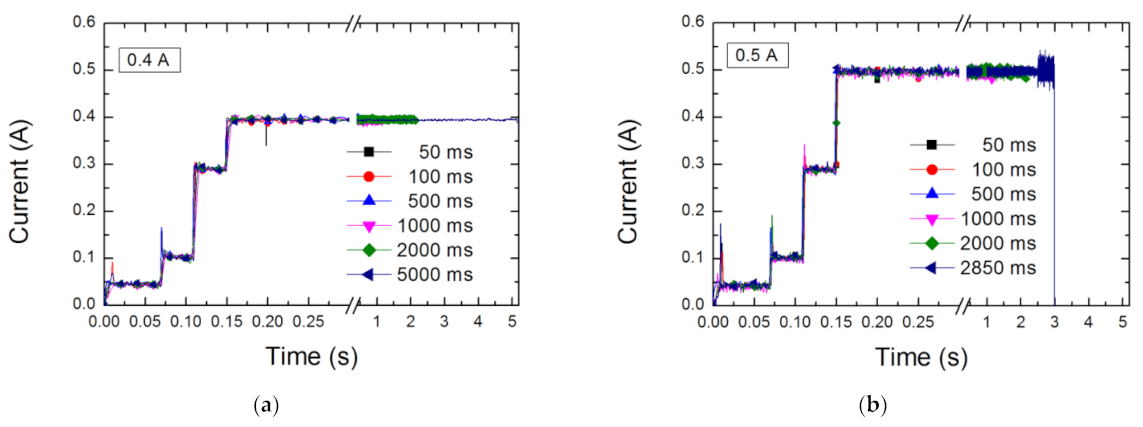
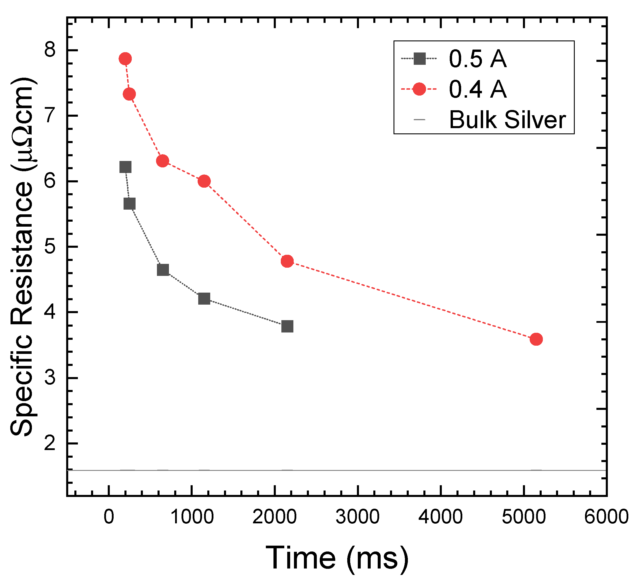
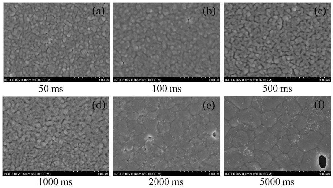
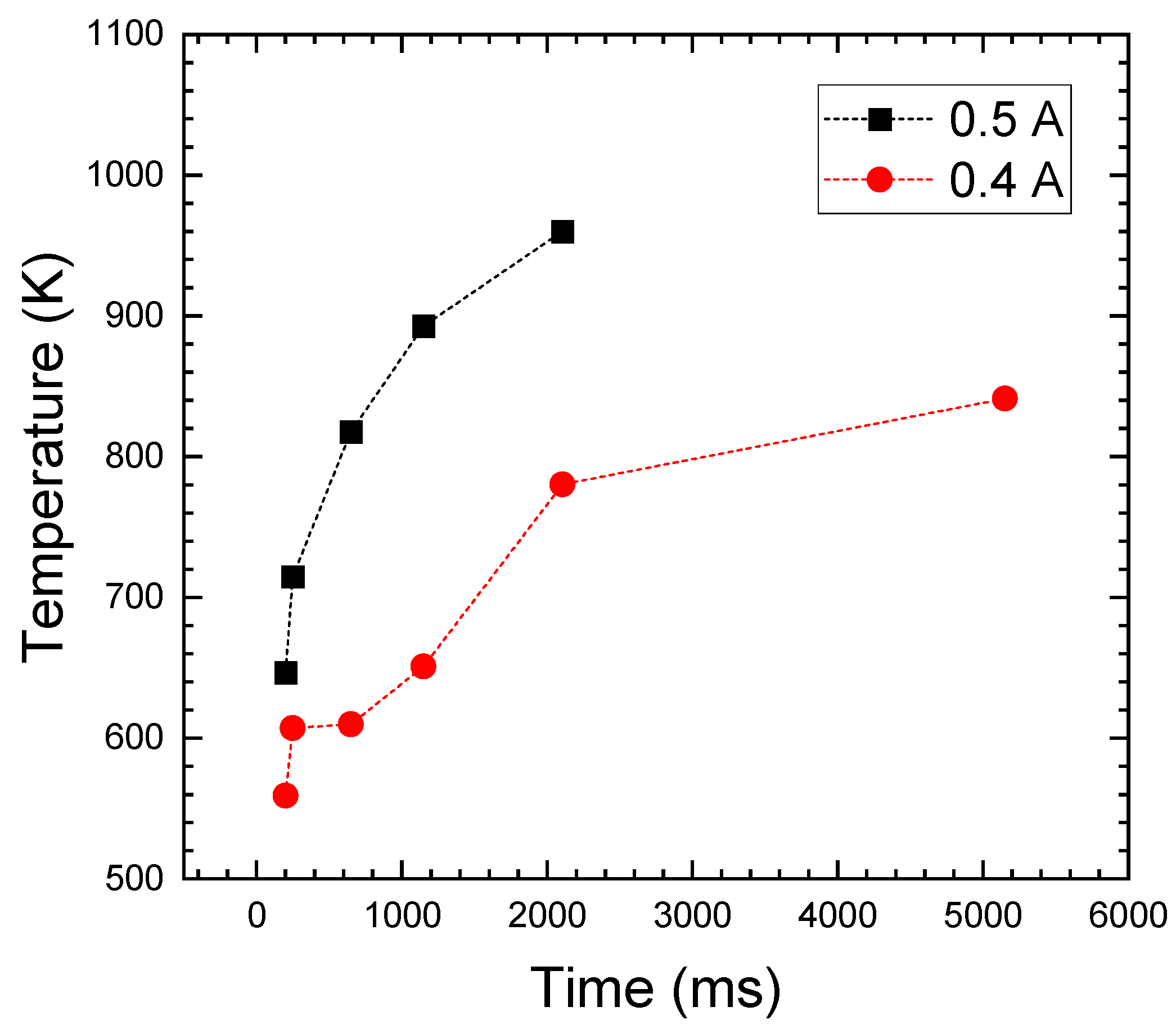
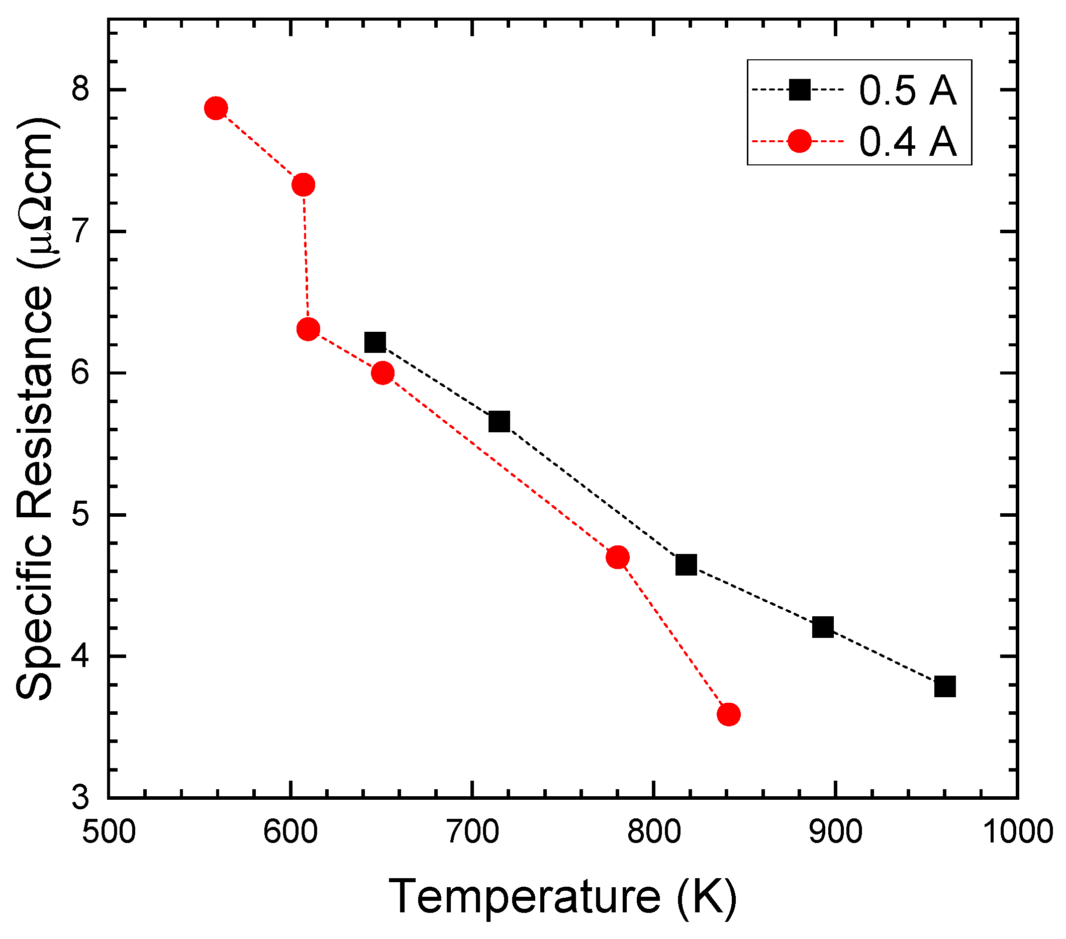
3. Results and Discussion
4. Conclusions
Author Contributions
Funding
Institutional Review Board Statement
Informed Consent Statement
Data Availability Statement
Conflicts of Interest
References
- Zschieschang, U.; Klauk, H.; Halik, M.; Schmid, G.; Dehm, C. Flexible organic circuits with printed gate electrodes. Adv. Mater. 2003, 15, 1147–1151. [Google Scholar] [CrossRef]
- Miller, M.S.; Davidson, G.J.E.; Sahli, B.J.; Mailloux, C.M.; Carmichael, T.B. Fabrication of elastomeric wires by selective electroless metallization of poly(dimethylsiloxane). Adv. Mater. 2008, 20, 59–64. [Google Scholar] [CrossRef]
- Makrygianni, M.; Kalpyris, I.; Boutopoulos, C.; Zergioti, I. Laser induced forward transfer of Ag nanoparticles ink deposition and characterization. Appl. Surf. Sci. 2014, 297, 40–44. [Google Scholar] [CrossRef]
- Liu, Q.; Xu, B.; Zhang, Y.; Wang, X.; Mei, X.; Wang, X. Picosecond laser sintering of silver paste printed by laser induced forward transfer. Opt. Laser Technol. 2021, 135, 106712. [Google Scholar] [CrossRef]
- Kim, S.; Lee, W.S.; Lee, J.; Park, I. Direct micro/nano metal patterning based on two-step transfer printing of ionic metal nano-ink. Nanotechnology 2012, 23, 285301. [Google Scholar] [CrossRef] [PubMed]
- Dziedzic, A.; Słobodzian, P. Modern microelectronic technologies in fabrication of RFID tags. Radioengineering 2011, 20, 21–187. [Google Scholar]
- Dziedzic, A. Thick film resistors with IrO2 and Calr×Ti1-xO3-examples of chemically reactive and unreactive systems. Microelectron. J. 1988, 20, 187–193. [Google Scholar] [CrossRef]
- Lee, H.H.; Chou, K.-S.; Huang, K.C. Inkjet printing of nanosized silver colloids. Nanotechnology 2005, 16, 2436–2440. [Google Scholar] [CrossRef]
- Rogers, J.A.; Paul, K.E.; Jackman, R.J.; Whitesides, G.M. Using an elastomeric phase mask for sub-100 nm photolithography in the optical near field. Appl. Phys. Lett. 1997, 70, 2658–2860. [Google Scholar] [CrossRef]
- Huang, S.Z.; Wu, K.Y. Health Risk Assessment of Photoresists Used in an Optoelectronic Semiconductor Factory. Risk Anal. 2019, 39, 2625–2639. [Google Scholar] [CrossRef] [PubMed]
- Calvert, P. Inkjet printing for materials and devices. Chem. Mater. 2001, 13, 3299–3305. [Google Scholar] [CrossRef]
- Theodorakos, I.; Zacharatos, F.; Geremia, R.; Karnakis, D.; Zergioti, I. Selective laser sintering of Ag nanoparticles ink for applications in flexible electronics. Appl. Surf. Sci. 2015, 336, 157–162. [Google Scholar] [CrossRef]
- Wong, W.S.; Salleo, A. Flexible Electronics: Materials and Applications; Springer Science+Business Media, LLC: New York, NY, USA, 2009; ISBN 0387743634. [Google Scholar]
- Ko, S.H.; Pan, H.; Grigoropoulos, C.P.; Luscombe, C.K.; Fréchet, J.M.J.; Poulikakos, D. All-inkjet-printed flexible electronics fabrication on a polymer substrate by low-temperature high-resolution selective laser sintering of metal nanoparticles. Nanotechnology 2007, 18, 345202. [Google Scholar] [CrossRef]
- Ko, S.H.; Pan, H.; Grigoropoulos, C.P.; Luscombe, C.K.; Fráchet, J.M.J.; Poulikakos, D. Air stable high resolution organic transistors by selective laser sintering of ink-jet printed metal nanoparticles. Appl. Phys. Lett. 2007, 90, 141103. [Google Scholar] [CrossRef] [Green Version]
- Noh, J.; Ha, J.; Kim, D. Femtosecond and nanosecond laser sintering of silver nanoparticles on a flexible substrate. Appl. Surf. Sci. 2020, 511, 145574. [Google Scholar] [CrossRef]
- Zenou, M.; Ermak, O.; Saar, A.; Kotler, Z. Laser sintering of copper nanoparticles. J. Phys. D Appl. Phys. 2014, 47, 025501. [Google Scholar] [CrossRef]
- Lee, B.; Kim, Y.; Yang, S.; Jeong, I.; Moon, J. A low-cure-temperature copper nano ink for highly conductive printed electrodes. Curr. Appl. Phys. 2009, 9, 157–160. [Google Scholar] [CrossRef]
- Kim, T.Y.; Hwang, J.Y.; Moon, S.J. Laser curing of the silver/copper nanoparticle ink via optical property measurement and calculation. Jpn. J. Appl. Phys. 2010, 49, 05EA091–05EA096. [Google Scholar] [CrossRef]
- Soltani, A.; Khorramdel Vahed, B.; Mardoukhi, A.; Mäntysalo, M. Laser sintering of copper nanoparticles on top of silicon substrates. Nanotechnology 2015, 27, 035203. [Google Scholar] [CrossRef] [PubMed]
- German, R.M. German, Sintering theory and practice. Chapitre 1996, 12–13, 68–74. [Google Scholar]
- Halonen, E.; Viiru, T.; Östman, K.; Cabezas, A.L.; Mantysalo, M. Oven sintering process optimization for inkjet-printed Ag Nanoparticle ink. IEEE Trans. Compon. Packag. Manuf. Technol. 2013, 3, 350–356. [Google Scholar] [CrossRef]
- Perelaer, J.; De Gans, B.J.; Schubert, U.S. Ink-jet printing and microwave sintering of conductive silver tracks. Adv. Mater. 2006, 18, 2101–2104. [Google Scholar] [CrossRef]
- Kim, D.; Moon, J. Highly Conductive Ink Jet Printed Films of Nanosilver Particles for Printable Electronics. Electrochem. Solid-State Lett. 2005, 8, J30–J33. [Google Scholar] [CrossRef]
- Choi, J.H.; Ryu, K.; Park, K.; Moon, S.J. Thermal conductivity estimation of inkjet-printed silver nanoparticle ink during continuous wave laser sintering. Int. J. Heat Mass Transf. 2015, 85, 904–909. [Google Scholar] [CrossRef]
- Bolduc, M.; Trudeau, C.; Beaupré, P.; Cloutier, S.G.; Galarneau, P. Thermal Dynamics Effects using Pulse-Shaping Laser Sintering of Printed Silver Inks. Sci. Rep. 2018, 8, 1418. [Google Scholar] [CrossRef] [PubMed] [Green Version]
- Kim, M.; Jee, H.; Lee, J. Photo-Sintered Silver Thin Films by a High-Power UV-LED Module for Flexible Electronic Applications. Nanomaterials 2021, 11, 2840. [Google Scholar] [CrossRef]
- Magdassi, S.; Grouchko, M.; Berezin, O.; Kamyshny, A. Triggering the sintering of silver nanoparticles at room temperature. ACS Nano 2010, 4, 1943–1948. [Google Scholar] [CrossRef]
- Allen, M.L.; Aronniemi, M.; Mattila, T.; Alastalo, A.; Ojanperä, K.; Suhonen, M.; Seppä, H. Electrical sintering of nanoparticle structures. Nanotechnology 2008, 19, 175201. [Google Scholar] [CrossRef] [PubMed]
- Moon, Y.J.; Lee, S.H.; Kang, H.; Kang, K.; Kim, K.Y.; Hwang, J.Y.; Cho, Y.J. Electrical sintering of inkjet-printed silver electrode for c-Si solar cells. PLoS ONE 2011, 6, e17209. [Google Scholar] [CrossRef]
- Alastalo, A.T.; Seppä, H.; Leppäniemi, J.H.; Aronniemi, M.J.; Allen, M.L.; Mattila, T. Modelling of nanoparticle sintering under electrical boundary conditions. J. Phys. D Appl. Phys. 2010, 43, 485501. [Google Scholar] [CrossRef]
- Tan, H.W.; Saengchairat, N.; Goh, G.L.; An, J.; Chua, C.K.; Tran, T. Induction Sintering of Silver Nanoparticle Inks on Polyimide Substrates. Adv. Mater. Technol. 2020, 7, 1900897. [Google Scholar] [CrossRef]
- Jang, S.; Lee, D.J.; Lee, D.; Oh, J.H. Electrical sintering characteristics of inkjet-printed conductive Ag lines on a paper substrate. Thin Solid Films 2013, 546, 157–161. [Google Scholar] [CrossRef]
- Lee, H.; Kim, D.; Lee, I.; Moon, Y.J.; Hwang, J.Y.; Park, K.; Moon, S.J. Stepwise current electrical sintering method for inkjet-printed conductive ink. Jpn. J. Appl. Phys. 2014, 53, 05HC07. [Google Scholar] [CrossRef]
- Moon, Y.J.; Kang, H.; Kang, K.; Moon, S.J.; Young hwang, J. Effect of Thickness on Surface Morphology of Silver Nanoparticle Layer During Furnace Sintering. J. Electron. Mater. 2015, 44, 1192–1199. [Google Scholar] [CrossRef]
- Kittel, C. Introduction to Solid State Physics, 8th ed.; John Wiley & Sons, Inc.: Hoboken, NJ, USA, 2005; ISBN 9783540938033. [Google Scholar]
- Kim, D.; Lee, I.; Yoo, Y.; Moon, Y.J.; Moon, S.J. Transient variation of a cross-sectional area of inkjet-printed silver nanoparticle ink during furnace sintering. Appl. Surf. Sci. 2014, 305, 453–458. [Google Scholar] [CrossRef]
- Wang, T.; Chen, X.; Lu, G.Q.; Lei, G.Y. Low-temperature sintering with nano-silver paste in die-attached interconnection. J. Electron. Mater. 2007, 36, 1333–1340. [Google Scholar] [CrossRef]
- Greer, J.R.; Street, R.A. Thermal cure effects on electrical performance of nanoparticle silver inks. Acta Mater. 2007, 55, 6345–6349. [Google Scholar] [CrossRef]
- Lee, D.G.; Kim, D.K.; Moon, Y.J.; Moon, S.J. Effect of temperature on electrical conductance of inkjet-printed silver nanoparticle ink during continuous wave laser sintering. Thin Solid Films 2013, 546, 443–447. [Google Scholar] [CrossRef]
- Kusy, A.; Listkiewicz, E. Percolation network for thick resistive films. Solid. State. Electron. 1988, 31, 821–830. [Google Scholar] [CrossRef]


| Parameters (Silver NP Ink) | Symbol | Values | Parameters (Glass Substrate) | Symbol | Values |
|---|---|---|---|---|---|
| Density | ρ1 | 5400 kg/m3 | Density | ρ2 | 2600 kg/m3 |
| Emissivity | ε1 | 0.01–0.02 | Emissivity | ε2 | 0.92 |
| Heat Capacity | cp,1 | 245 J/kg·K | Heat Capacity | cp,2 | 840 J/kg·K |
| Convective Heat Transfer Coefficient | h | 10 W/m2·K | Stephan–Boltzmann Constant | σ | 5.67 × 10⁻⁸ W/m2K4 |
| Thermal Conductivity | k1 | Equation (2) | Thermal Conductivity | k2 | 1.05 W/m·K |
| Width | w1 | 130 µm | Width | w2 | 2.4 cm |
| Thickness | t1 | 300 nm | Thickness | t2 | 0.5 cm |
Publisher’s Note: MDPI stays neutral with regard to jurisdictional claims in published maps and institutional affiliations. |
© 2021 by the authors. Licensee MDPI, Basel, Switzerland. This article is an open access article distributed under the terms and conditions of the Creative Commons Attribution (CC BY) license (https://creativecommons.org/licenses/by/4.0/).
Share and Cite
Lee, I.; Hussain, A.; Lee, H.-L.; Moon, Y.-J.; Hwang, J.-Y.; Moon, S.-J. The Effect of Current Supply Duration during Stepwise Electrical Sintering of Silver Nanoparticles. Metals 2021, 11, 1878. https://doi.org/10.3390/met11111878
Lee I, Hussain A, Lee H-L, Moon Y-J, Hwang J-Y, Moon S-J. The Effect of Current Supply Duration during Stepwise Electrical Sintering of Silver Nanoparticles. Metals. 2021; 11(11):1878. https://doi.org/10.3390/met11111878
Chicago/Turabian StyleLee, Iksang, Arif Hussain, Hee-Lak Lee, Yoon-Jae Moon, Jun-Young Hwang, and Seung-Jae Moon. 2021. "The Effect of Current Supply Duration during Stepwise Electrical Sintering of Silver Nanoparticles" Metals 11, no. 11: 1878. https://doi.org/10.3390/met11111878
APA StyleLee, I., Hussain, A., Lee, H.-L., Moon, Y.-J., Hwang, J.-Y., & Moon, S.-J. (2021). The Effect of Current Supply Duration during Stepwise Electrical Sintering of Silver Nanoparticles. Metals, 11(11), 1878. https://doi.org/10.3390/met11111878