Abstract
Synchrotron X-ray Scanning Tunneling Microscopy (SX-STM) is a novel imaging technique capable of providing real space chemically specific mapping with a potential of reaching atomic resolution. Determination of chemical composition along with ultra-high resolution imaging by SX-STM can be realized through excitation of core electrons by incident X-rays when their energy is tuned to an absorption edge of a particular atom during raster scanning, as is done in the conventional STM experiments. In this work, we provide a brief summary and the current status of SX-STM and discuss its applications for material science. In particular, we discuss instrumentation challenges associated with the SX-STM technique and present early experiments on Cu doped ZrTe3 single crystals.
1. Introduction
Accurate determination of surface structure and chemical composition of materials at their interfaces and surfaces allows us to design and engineer material systems with specific physical properties and desired functionalities. Scanning tunneling microscopy (STM) is a conventional tool used to atomically resolve surface morphology and conduct spectroscopic measurements on conductive surfaces [1,2]. A typical STM instrument includes a conductive tip on a scanner (XYZ piezo-tube), a sample stage, and a set of electronics with feedback loops to control either tunneling current or the distance (d, typically less than 1 nm) between the sample surface and the tip, to image the surface contour structure. However, conventional STM only detects electrons in the valence or conduction bands but does not provide direct chemical composition of a conductive surface, which relies on excitation and detection of core-level electrons. Currently, only electron microscopy, such as scanning transmission electron microscopy-energy dispersion X-ray spectroscopy (STEM-EDS), high-angle annular dark-field scanning transmission electron microscopy-STEM—Electron energy loss spectroscopy (HADDF-STEM-EELS) and transmission electron microscopy—selected area electron diffraction (TEM-SAED), can be used in a limited number of applications for ultra-high resolution elemental mapping [3]. Synchrotron X-ray Scanning Tunneling Microscopy (SX-STM) is complementary to those existing microscopic methods and enables ultra-high resolution elemental mapping. SX-STM has been developed and pursued by several research groups [4,5,6,7]. During a STEM or TEM measurement, a sample is exposed to primary electrons with energies higher than 100 keV; while during an SX-STM measurement, a sample surface is exposed to X-ray photons. A SX-STM measurement is conducted when monochromatic X-ray beam illuminates the tip-sample gap area, while an SX-STM tip is raster scanned across the sample surface to acquire conventional STM data. Chemical sensitivity of SX-STM relies on excitation of core electrons in surface atoms by incident X-rays when their energy is tuned to an absorption edge of a specific element on the surfaces. As opposed to the conventional X-ray fluorescence imaging where the resolution is determined by the focusing properties of X-ray optics, [8,9] in SX-STM, a typical X-ray beam size is much bigger than the tip-sample gap area (from microns to sub-micrometers), therefore requirements for X-ray focusing are relaxed. During SX-STM measurements, photoelectrons are also excited along with the core-level electrons. Those photoelectrons contribute as an additional tip current and interfere with the tunneling current from specific atoms. The photoelectrons primarily include Auger electrons from the de-excitation after photoionization, secondary photoelectrons from photo-absorption, and secondary Auger electrons from the relaxation of secondary excited atoms. During SX-STM measurements, the tip current is always a superposition of various constituents and can be expressed as follows:
where Itunneling is the conventional tunneling currents controlled by a feedback loop, and Itunneling, X-ray is the X-ray excited/enhanced tunneling current generated from tunneling electrons of the tip-surface area being boosted by X-ray under the tip. Iphoto-ejected, X-ray is the photocurrent generated by X-ray excited electron across the local tunneling gap that has enough energy to leave the sample surface and be detected by the tip. Itunneling provides the morphology information about the sample surface, while (Itunneling, X-ray + Iphoto-ejected, X-ray) both provide the chemical information, with the former being localized and the latter being a contribution from the X-ray illuminated area of a sample. All three components of the tunneling current must be separated in order for the STM feedback system to stay in the tunneling regime (typical tip-sample separation ≤1 nm). Table 1 provides a summary of various SX-STM experimental regimes with corresponding tunneling current contributions.
ISX-STM = Itunneling + Itunneling, X-ray + Iphoto-ejected, X-ray

Table 1.
Synchrotron X-ray Scanning Tunneling Microscopy (SX-STM) experimental regimes and corresponding tunneling current contributions.
In the following sections, we provide a brief summary and current status of SX-STM technique, and then discuss its application for studies in materials science. We first focus on the developments in instrumentation which enable detection of X-ray assisted tunneling current, followed by a few examples, including preliminary measurements on Cu doped ZrTe3 single crystals.
2. Materials and Methods—Smart Tips and SX-STM Instrumentation
2.1. Smart Tips
When the X-ray energy is tuned to an absorption edge of a particular element on a sample surface, along with core-level electrons from the tip-surface area right under the STM tip, photo-electrons are also excited and collected from a large area of a sample, resulting in Iphoto-ejected, X-ray. Conventional STM tips are fabricated out of metals, and if they are exposed to X-rays, it results in additional photoelectric current detected by the STM electronics. The STM tip cannot distinguish between various electronic contributions, therefore photoemission processes interfere with quantum tunneling and result in a background signal, making localized detection of chemically specific tunneling current extremely difficult. In order to reduce the background photoelectron current, and ultimately improve SX-STM spatial resolution, one needs to minimize the surface area of an STM tip exposed to electrons that are ejected from the sample surface, i.e., to fabricate “smart tips”. A “smart tip” refers to a tip that is entirely coated with shielding/insulating film except for a tip apex. An insulating film assists in reducing the background current signals introduced by photo-ejected electrons and collected by the sidewalls of a tip. Glass-coated tungsten (W) and silica (SiO2)-coated W tips have been fabricated and 10 nm spatial resolution has been demonstrated [10,11]. However, W oxidizes easily during the fabrication process therefore chemically inert PtIr tips have been developed. Different approaches have been used to coat PtIr tips, which include boron nitride deposition (BN) or SiO2 by e-beam deposition [7,12,13]. In the section below we review various approaches that have been developed and applied to fabrication of smart tips in the past five years [4,14,15,16,17,18].
2.1.1. Insulator-Coated CNT Smart Tips
Our team has developed and fabricated a multi-walled carbon nanotubes (MWCNT) based smart tips using plasma enhanced chemical vapor deposition (PECVD) and focused ion beam milling (FIB) [19]. Pt90Ir10 tips were electrochemically etched from a clean wire with a diameter of 0.250 mm using CaCl2 aqueous solution, to form a sharp and symmetric apex. After cleaning with hot deionized water and methanol, SiO2 films with a thickness of 100 nm–3 μm were deposited on the wires by plasma enhanced chemical vapor deposition (PECVD), using SiH4:N2:N2O gas mixtures. The thickness of SiO2 was controlled by the PECVD process time. The tips were flipped every 50 nm deposition at a deposition rate of 2 nm/s, to assure uniform coating. A two-step FIB process was applied to further fabricate the tips. First, Ga+ ions from FIB (30 keV, 90 pA) were impinged normal to the tip axis, to expose the radial cross section of the tip apex. Second, Ga+ ions were impinged at normal incidence to the radial cross section, and then a series of donut-shape writing patterns, with decreasing diameter and ion beam current to fabricate a Pt90Ir10 pillar. The fabricated Pt90Ir10 tip was then mounted on a micromanipulator as part of a conductive circuit inside a dedicated SEM. By applying a small DC voltage to both the CNT and pillar, and due to electrostatic force, a CNT was brought to the Pt90Ir10 tip and then aligned in a normal way to the tip apex, followed by using higher applied power to ensure welding of CNT to the tip. The contact of CNT with Pt90Ir10 pillar was further strengthened by localized Pt deposition from ion beam assisted CVD (FIB). The Pt90Ir10 pillar was then covered with SiO2 through localized growth by electron beam assisted chemical vapor deposition, using tetraethyl orthosilicate (TEOS), which was applied in situ through a nozzle in close proximity to the tip, along with H2O. The SiO2 coating formed from PECVD and repaired by TEOS is rigid and uniform, and strongly reduces the number of photo-ejected electrons. A fabricated tip is shown in Figure 1a. The developed CNT-based smart tips demonstrated good performance in reducing the tip current, when compared to when using a bare etched tip, see Figure 1b,c.
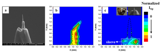
Figure 1.
(a) SEM images of a fabricated 0.25 mm Pt90Ir10 tip—230 nm SiO2 attached with a multi-walled carbon nanotube, MWCNT (580 nm in length and 20 nm in diameter) and (b) Normalized photocurrent map of the bare Pt90Ir10 tip (0.5 mm in diameter). The result shows that photocurrent is detected by the whole tip apex; (c) Normalized photocurrent map of the “smart tip” (0.25 mm Pt90Ir10 wire coated with 350 nm SiO2, attached with a MWCNT, as shown in the insert). The photocurrent of the smart tip is drastically reduced after being coated with SiO2. The photocurrents in (b) and (c) are normalized with respect to the maximum current detected in the same plot [19].
2.1.2. Coaxially Shielded STM Tips
Metal-insulator-metal (MIM, PtIr-SiO2-Ti/Au) tips: A MIM coaxial smart tip has a metallic PtIr core etched from 0.25 mm thick PtIr wire, and the core was covered by an insulating SiO2 layer. In addition, an outermost conducting Au/Ti (250 nm/20 nm) shell was deposited onto the surface of the insulating oxide (total thickness of outer insulating/metal layer is ~1 µm). The outermost Au/Ti metal layer serves as an electrical contact for grounding to prevent undesired charging effects, and as a “shield” to reduce the magnitude of X-ray excited electron current detected at the tip when biased with a voltage [20,21]. The PtIr tip apex was then exposed after FIB milling. MIM tips have been used in a number of applications listed in Table 2, which provides an overview of various smart tips and their respective applications that have been used since 2014.
Table 2.
Developed smart tips and their applications to the SX-STM studies since 2014.
Metal-Polymer coated Metal (MPM, PtIr-PV-Ti/Au) tips: Based on a method used to fabricate tips for electrochemical STM [25], polymer coated SX-STM tips have been developed [18]. An electrochemically etched 0.25 mm PtIr wire was pushed through a droplet of polyethylene-vinylacetate-based glue gun wax (PV) at 80 °C. The shield coating was applied by radiofrequency sputter deposition of a Ti seed layer followed by 100 nm Au for the polymer tips. The tip apex was then shaped using FIB milling. The coating thickness was not uniform, i.e., thicker in the middle of a tip (1 mm) and thinner at the apex (a few hundred nanometers). Atomic steps has been observed during STM imaging of Au(111) when using an MPM coaxial tip at 12.1 keV photon energy [18].
2.2. SX-STM Instrumentation and Methods
SX-STM experiments are rather complex and involve synchrotron radiation instrumentation combined with an STM scanning microscope. Typically, a complete endstation needs to be developed and installed at a given beamline. Since detection of SX-STM currents is associated with distinguishing between the actual tunneling current and a much larger photoelectron current, lock-in techniques are widely used to improve the signal-to-noise ratio [6,18,23]. Dedicated UHV compatible choppers along with topographic filters have been developed to modulate the incoming X-ray beam and provide a reference signal for the lock-in amplifiers (LIA) [26]. As shown in Figure 2a, during an SX-STM experiment the convoluted tip current is first fed into a lock-in amplifier (typically locking at a chopping frequency of 3 kHz or higher) and the output of LIA is directly proportional to the X-ray induced current signal. The tip current is then fed into a topological filter to cut off the high frequency signal and yield Itunneling, which is then fed into a feedback loop of an STM controller [21,22]. Moreover, an additional LIA can be used to record the signal originating from a sample simultaneously.
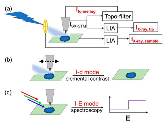
Figure 2.
Schematic of an SX-STM experiment (a); SX-STM modes and their expected results (b) I-d mode and (c) I-E mode.
A number of SX-STM instruments have been designed and constructed in the recent years. A low temperature (LT) SX-STM system has been developed at the Advanced Photon Source (APS), Argonne National Laboratory [23]. The instrument is now part of the XTIP beamline at 4-ID-E (Rose et al., manuscript in preparation). The system is equipped with a manipulator and a dedicated vacuum suitcase (base pressure <10−10 Torr) to allow transferring of samples and smart tips without compromising vacuum inside the microscope chamber. In addition, in situ cleaving of samples is possible. Another SX-STM microscope has been developed and installed at the European Synchrotron Radiation Facility (ESRF) by Mom et al. [18] and is used for high pressure (operando) measurements. The system comprises of a UHV chamber with a high-pressure cell/reactor on top and placed in a controlled gas atmosphere at pressures up to 1.1 bar. It uses a single piezo tube both for coarse approach of the tip to the sample surface and for scanning surfaces. The piezo tube is separated from the gas environment by a polyimide cap and a Viton seal and enables measurements down to 8 keV photon energy. The X-ray chopper frequency is set to ~10 kHz to minimize the current noise under operando conditions.
During the first step of an SX-STM experiment, a smart tip is aligned with respect to the incident X-ray beam [12]. The alignment of a tip typically requires the SX-STM chamber to have adequate degrees of motion, i.e., horizontal, vertical and rotations. During the initial coarse alignment, the tip is illuminated by incident X-rays and is placed far away from the sample. The photocurrent is monitored and recorded as a function of tip position. The chamber is scanned, and the highest recorded current indicates the maximum X-ray illumination [23]. During the next step, the smart tip is brought close to the sample surface (tunneling mode) and SX-STM scanning experiment is initiated.
To measure the X-ray excited element specific electrons down to the atomic-scale spatial resolution, two experimental methods, “I-E” and “I-d”, are used and both are under constant-current mode, as shown in Figure 2b,c. The “I-E” spectroscopy is collected by taking the X-ray induced tip/sample current as a function of X-ray energy, [21] when a tip stays in point mode in the tunneling region. The “I-d” spectroscopy measures the tip/sample currents as a function of lateral displacement, the same way as in conventional STM tip raster-scanning experiments; it reflects local changes in current components depending on the chemical nature of the materials. For example, both SX-STM spectroscopies and spatial dependent X-ray induced absorption have been measured at the atomic scale between an Au(111) surface and a 25.6 nm2 × 2 atomic layer Co nanocluster boundary with a tip located ~0.5 nm above the Au(111) surface [21]. An increased current was observed from the I-E plot on the Co nanocluster when the energy of X-rays was tuned to be higher than Co K-edge at 7.709 keV. Using the currents detected from both the sample surface and the tip, the current difference, ΔI, between currents detected at photon energies higher and lower than Co K-edge, has been calculated. The tunneling current enhanced by the X-rays can then be determined from ΔI at the sample surface, yielding the current components listed in Table 1.
3. Results and Discussions of Applications—SX-STM Spectroscopy and Preliminary Elemental Mapping on ZrTe3 Single Crystal
Scientific interest in interplay of superconductivity (SC) and charge-density waves (CDW), the two contrasting electronic states that potentially coexist in CDW superconductors, has emerged since the discovery of broken-symmetry ground states in high-temperature superconducting cuprates [27]. The interplay between CDW and SC is important and can be the key limiting factor defining the magnitude of the critical temperature [28,29]. ZrTe3 is one of the chainlike chalcogenide charge-density-wave (CDW) materials. The formation of its CDW condensate at TCDW is along the crystallographic direction perpendicular to the b-axis Zr-Zr chains [30]. CDW and filamentary superconductivity coexist in ZrTe3 due to the multiband nature of the Fermi surface [31,32]. Like its parent compound ZrTe3, CDW and superconductivity coexist along the a axis for Cu0.05ZrTe3 single crystal [33]. Most recent studies show the intercalation of Cu or Ni suppresses the CDW state, with TCDW falling from 63 K for ZrTe3 down to 41 K for Cu0.05ZrTe3 and ~50 K for Ni0.05ZrTe3 along the a axis [31,34]. In addition, the intercalation by Cu and Ni of ZrTe3 has been suggested as an alternative method to externally applied pressure for inducing superconductivity [33,35,36]. Intercalation of ZrTe3 with metals raises the bulk Tc from less than 2 K for ZrTe3 to 3.8 K in Cu-doped ZrTe3 single crystal, and to 3.1 K in the Ni0.05ZrTe3 [31,33,36]. However, little is known about the mechanisms of how these dopants affect the CDW and superconductivity states, as well as the properties of the materials. Therefore, mapping of elements at the nanoscale on the surface of doped ZrTe3 crystals becomes important and has a potential to shed light on correlations between superconducting properties and dopants distribution within a sample.
Cu0.05ZrTe3 single crystals were grown from pure elements in a mole ratio of Cu:Zr:Te = 0.05:1:3 with 5 mg/cm3 iodine sealed in an evacuated quartz tube. After heating at 973 K, the furnace gradient was kept between 1023 and 923 K for two days. The freshly cleaved sample presents a layered structure and contains large flat terraces on its surface, without any obvious microstructure, as seen in the insert of Figure 3a (data collected at JEOL 7600F SEM microscope). The chemical composition of the single crystal is determined by energy dispersive spectroscopy (EDS) analysis and is shown in Figure 3a. Only Cu, Zr, and Te are present on the surface, with trace amount of the carbon contamination, from the EDS analysis. The Cu concentration (averaged over seven measurements) is calculated to be 0.050 ± 0.020.
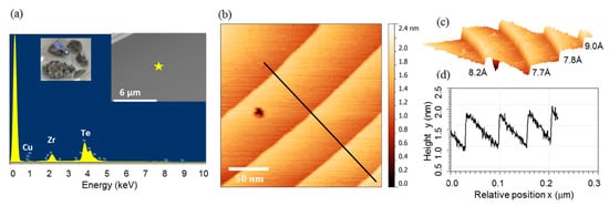
Figure 3.
(a) Scanning electron microscope (SEM) images, and energy-dispersion X-ray spectrum (EDS) of Cu0.05ZrTe3, the inserts are a photo image of the crystal (left) and a SEM image (right) in which the star is the sampling position of EDS. (b) STM image of Cu0.05ZrTe3 (200 nm × 200 nm) using W tip, Itunneling = 1.0 nA, bias = 20 mV, various terraces are exhibited; (c) 3D image of (b), the image is rotated (ϕ = 60°) and tilted (ϑ = −75°) from (b). (d) line profile of (b), step size = 8.2 ± 0.5 Å (smaller than 1.0 nm of the c-axis but close to the metal-metal distance of ZrTe3 surface at 7.1 Å).
The surface morphology was further characterized with a conventional UHV- STM (RHK 7500 Variable Temperature UHV Scanning Tunneling/Atomic Force Microscope system) at room temperature under pressures of <5 × 10⁻¹⁰ Torr, with electrochemically etched tungsten tips at 20 mV bias and 1.0 nA tunneling current in a constant current mode. The crystal was in-situ cleaved at low pressure (10−6 Torr) inside the load lock and then transferred to the STM stage (10−9 Torr), to ensure the surface cleanness. The STM image shows large flat terraces with a size on the order of 50–100 nm, which is consistent with the SEM results. Pure ZrTe3 van der Waals surfaces have defects along the ZrTe3[100] direction [37]. Similar to its parent compound, defects are found in the Cu doped ZrTe3 crystal in Figure 3b,c. The depression observed in one of the terraces, as shown in the 3D image, is attributed to a defect generated from the crystal growth, since deep steps on such a small scale cannot be produced by an imperfect cleavage [15]. The average step height for a single layer is 8.2 ± 1.0 Å (Figure 3c), corresponding approximately to those of complete Te–Zr–Te sandwiches, ~10.11 Å [38]. This is in agreement with XPD data that intercalation of Cu does not change the original crystal structure, only leads to larger a and c axes with the b axis (Zr chains) unchanged [31,38]. Upon doping, Cu is more likely to intercalate than to substitute atoms located in the van der Waals bonded crystallographic layers, due to the smaller atomic size of Cu compared to that of Zr [31,33].
After initial characterization of Cu0.05ZrTe3, I-E experiments have been conducted using LT-SX-STM at 26-ID beamline of the Advanced Photon Source at Argonne National Lab. A typical size of the sample crystal was 2 × 3 × 0.06 mm3 elongated along the b axis (Figure 3a), which was 50 times smaller than that of the mounting plate, thus, spectroscopy mode of SX-STM was applied first to ensure optimized alignment of the sample surface with respect to the X-ray beam. A dedicated vacuum suitcase (base pressure 10−9 Torr) was used to transfer Cu0.05ZrTe3 and smart coaxial tips into the SX-STM system. The crystal was in situ cleaved inside of the sample suitcase prior to being transferred into the main chamber of the LT-SX-STM system. A MIM coaxial smart tip, PtIr-SiO2-Au/Ti [14], was used to generate an SX-STM image.
Figure 4a,b represent spectroscopy scans across the Cu K-edge with the tip tunneling over Cu(111) (panel a) as a reference, and Cu0.05ZrTe3 (panel b) [14]. The illuminated sample area is about 500 × 500 μm2 and sample bias voltage was set at −1 V. The tip current spectrum of Cu0.05ZrTe3 in Figure 4b exhibits a peak caused by the Cu K1s absorption edge, when the tip is parked and tunneling over a single random point on the surface. The measurement suggests that SX-STM has adequate sensitivity to detect low concentrations (<5%) of Cu in Cu0.05ZrTe3 crystals. In addition, on the contrary to the increased tip and sample currents at the Cu K-edge, the filtered current used for the feedback (Itunneling) remains stable but noisy with the topo filter being installed (Figure 4c), the value 0.9 nA agrees well with the STM setpoint current of 1.0 nA that was selected for this particular experiment. This measurement indicates that topography and chemical contrast datasets are well separated. The tip and sample currents exhibit characteristic features of the extended X-ray fine structure (EXAFS) spectrum of copper on Cu(111), which is not observed in Cu0.05ZrTe3 (Figure 4b), this is in agreement with the results from EDS showing that Cu is not evenly distributed on the surface and does not form any crystalline structure.
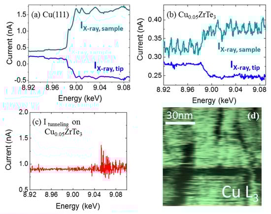
Figure 4.
Spectroscopy scans across the Cu K-edge with the tip tunneling over Cu(111) ((a), [14]) and Cu0.05ZrTe3 (b), where simultaneously derived signals from the lock-in amplifiers LIA-sample (IX-ray, sample) and LIA-tip (IX-ray, tip) exhibit the characteristic EXAFS spectrum of copper, which is not observed by the Cu0.05ZrTe3. Note IX-ray, sample in the Cu0.05ZrTe3 spectrum appears to be noisier due to potential instabilities in the beamline. Bias is −1V, tunneling current is 1.0 nA for Cu0.05ZrTe3 and 0.5 nA for Cu(111); (c) tunneling current separated from the sample and tip currents collected from the Cu0.05ZrTe3; (d) SX-STM image (I-d mode) obtained from Cu0.05ZrTe3 under X-ray illumination at the Cu L3 absorption edge using the XTIP microscope. The dark areas suggest depletion of Cu at some surface areas.
Initial measurements presented here are the first demonstration that SX-STM can be used to investigate superconducting samples. SX-STM has demonstrated adequate sensitivity to detect Cu on the surface of a sample with the Cu concentration being less than 5%. First preliminary imaging experiments, using I-d mode, at room temperature have been performed using the XTIP endstation instrument (APS), shown in Figure 4d. Resonant X-ray excitations at the Cu L3 absorption edge yield an imaging contrast, suggesting that the Cu distribution is inhomogeneous at the nanoscale. The black areas (low X-ray exited current) indicate regions of Cu depletion at the surface. As a next step, more quantitative and detailed surface mapping of Cu distribution needs to be performed. With continuing development in SX-STM, it has the potential to correlate spatial distribution of Cu atoms with properties of a CDW Cu-doped ZrTe3 superconductor.
4. Conclusions and Outlook
SX-STM is a novel technique capable of chemically specific imaging at the nanometer scale, with a potential of achieving single atom resolution. Along with chemically specific mapping, SX-STM enables highly localized spectroscopic measurements. Recent developments in fabrication of smart tips along with construction of the dedicated end-stations at various synchrotron facilities allowed us to investigate different materials science phenomena, which include elemental mapping of metallic and ferromagnetic structures, highly localized XMCD on LSMO/LNO superlattices, operando absorption measurements on Au(111), and preliminary investigations of Cu distribution in the Cu0.05ZrTe3 superconductors (presented in this work). Some of other applications are summarized below.
a. Local X-ray magnetic dichroism (XMCD) using soft X-rays: Circularly polarized X-rays provides an opportunity to probe magnetic properties of a sample surface in addition to collecting elemental and topographic information [23,24,39,40]. Left spin of X-rays (LCP) will enhance the spin up electrons, while right spin of X-rays (RCP) helps spin down electrons, to leave and then reach the tip. Therefore, circularly polarized radiation along with a tunneling tip allows for local magnetic characterization with ultra-high spatial resolution. In addition, it also provides magnetic contrast, even with a non-magnetic tip, which is required in conventional spin-polarized STM. X-ray magnetic circular dichroism of LSMO/LNO superlattices have been studied at low temperatures [23], and magnetism at buried interface along with near edge X-ray absorption fine structure (NEXAF) were evaluated. The study suggested that magnetism has been induced by the LNO/LSMO interface through the charge transfer and interfacial strain, while no interfacial magnetism was found for LSMO/LNO superlattice [23].
b. Operando study of SX-STM imaging: Mom et al. studied Au(111) using an Au/polymer coaxial tip at 800 mbar Ar, 12.1 keV X-ray beam chopped at 10 kHz [18]. The SX-STM image demonstrated atomic step resolution on Au(111) and 1 nm lateral resolution distinguished from the step width, which is decreased to approximately 5 nm by interference from vibrational and electronic noises. This work demonstrates initial realization of operando X-ray absorption measurements with nanometer-scale spatial resolution.
c. SX-STM elemental mapping: A number of earlier works have demonstrated chemically specific high spatial resolutions imaging in metallic samples. For example, Okuda et al. showed ~10 nm mapping on checkerboard-patterned Ni and Fe samples when X-ray photon energies were tuned to above and below the Ni (Fe) L absorption edge. The research team utilized glass-coated W tips [41]. Saito et al. showed that Cu islands (>100 nm2) embedded into Ge(111) 2 × 8 surface can be spatially resolved by detecting changes in the tip current (∼10 pA) when scanned laterally [42].
In summary, further developments in SX-STM field (such as construction of dedicated beamlines or beamline branches similar to XTIP at APS along with further instrumentation refinements) will enable application of the technique to a broad range of materials science problems, which include localized magnetism, superconductivity, and the development of energy storage materials i.e., hierarchical structured materials, mesoporous oxides and carbon nanocages [43,44,45,46].
Author Contributions
Conceptualization, H.Y. and E.N.; Data curation, H.Y., N.S., X.Z., D.R., X.T., W.X. and C.P.; Formal analysis, V.R.; Funding acquisition, E.N.; Methodology, H.Y. and V.R.; Project administration, E.N.; Resources, X.T., C.P. and V.R.; Validation, N.S.; Visualization, H.Y.; Writing—Original draft, H.Y.; Writing—Review & editing, E.N.
Funding
This research received no external funding.
Acknowledgments
This work was supported by the Laboratory Directed Research and Development Program of Brookhaven National Laboratory and was performed using resources of the National Synchrotron Light Source II and the Center for Functional Nanomaterials, a U.S. Department of Energy (DOE) Office of Science User Facilities operated for the DOE Office of Science by Brookhaven National Laboratory, under Contract No. DE-SC0012704. Work at the Advanced Photon Source and the Center for Nanoscale Materials was supported by the U. S. Department of Energy, Office of Science, Office of Basic Energy Sciences, under Contract No. DE-AC02-06CH11357. This work was partially supported through Laboratory Directed Research and Development program at Brookhaven National Laboratory. Hui Yan would like to thank University of Louisiana at Lafayette.
Conflicts of Interest
The authors declare no conflict of interest.
References
- Binnig, G.; Rohrer, H.; Gerber, C.; Weibel, E. Tunneling through a controllable vacuum gap. Appl. Phys. Lett. 1982, 40, 178–180. [Google Scholar] [CrossRef]
- Binnig, G.; Rohrer, H. Scanning tunneling microscopy. IBM J. Res. Dev. 1986, 30, 355–369. [Google Scholar]
- Tanaka, N. Electron Nano-Imaging: Basics of Imaging and Diffraction for TEM and STEM; Springer: Heidelbeg, Germany, 2017; ISBN 9784431565000. [Google Scholar]
- Chan, Y.L.; Liang, X.; Wu, T.H.; Lu, D.A.; Luo, M.F.; Hsu, Y.J.; Wei, D.H. The development of synchrotron-assisted scanning probe microscopy at NSRRC. J. Phys. Conf. Ser. 2013, 463, 012035. [Google Scholar] [CrossRef]
- Matsushima, T.; Okuda, T.; Eguchi, T.; Ono, M.; Harasawa, A.; Wakita, T.; Kataoka, A.; Hamada, M.; Kamoshida, A.; Hasegawa, Y.; et al. Development and trial measurement of synchrotron-radiation-light-illuminated scanning tunneling microscope. Rev. Sci. Instrum. 2004, 75, 2149–2153. [Google Scholar] [CrossRef]
- Saito, A.; Maruyama, J.; Manabe, K.; Kitamoto, K.; Takahashi, K.; Takami, K.; Yabashi, M.; Tanaka, Y.; Miwa, D.; Ishii, M.; et al. Development of a scanning tunneling microscope for in situ experiments with a synchrotron radiation hard-X-ray microbeam. J. Synchrotron Radiat. 2006, 13, 216–220. [Google Scholar] [CrossRef] [PubMed]
- Rose, V.; Freeland, J.W.; Gray, K.E.; Streiffer, S.K. X-ray-excited photoelectron detection using a scanning tunneling microscope. Appl. Phys. Lett. 2008, 92, 193510. [Google Scholar] [CrossRef]
- Nazaretski, E.; Yan, H.; Lauer, K.; Bouet, N.; Huang, X.; Xu, W.; Zhou, J.; Shu, D.; Hwu, Y.; Chu, Y.S.; et al. Design and performance of an X-ray scanning microscope at the Hard X-ray Nanoprobe beamline of NSLS-II. J. Synchrotron Radiat. 2017, 24, 1113–1119. [Google Scholar] [CrossRef] [PubMed]
- Yan, H.; Bouet, N.; Zhou, J.; Huang, X.; Nazaretski, E.; Xu, W.; Cocco, A.P.; Chiu, W.K.S.; Brinkman, K.S.; Chu, Y.S. Multimodal hard X-ray imaging with resolution approaching 10 nm for studies in material science. Nano Futures 2018, 2, 011001. [Google Scholar] [CrossRef]
- Akiyama, K.; Eguchi, T.; An, T.; Hasegawa, Y.; Okuda, T.; Harasawa, A.; Kinoshita, T. Fabrication of a glass-coated metal tip for synchrotron-radiation-light- irradiated scanning tunneling microscopy. Rev. Sci. Instrum. 2005, 76, 083711. [Google Scholar] [CrossRef]
- Saito, A.; Takahashi, K.; Takagi, Y.; Nakamatsu, K.; Hanai, K.; Tanaka, Y.; Miwa, D.; Akai-kasaya, M.; Shin, S.; Matsui, S.; et al. Study for noise reduction in synchrotron radiation based scanning tunneling microscopy by developing insulator-coat tip. Surf. Sci. 2007, 601, 5294–5299. [Google Scholar] [CrossRef]
- Rose, V.; Wang, K.; Chien, T.; Hiller, J.; Rosenmann, D.; Freeland, J.W.; Preissner, C.; Hla, S.W. Synchrotron X-ray scanning tunneling microscopy: Fingerprinting near to far field transitions on Cu(111) induced by synchrotron radiation. Adv. Funct. Mater. 2013, 23, 2646–2652. [Google Scholar] [CrossRef]
- Rose, V.; Chien, T.Y.; Hiller, J.; Rosenmann, D.; Winarski, R.P. X-ray nanotomography of SiO2-coated Pt90Ir10 tips with sub-micron conducting apex. Appl. Phys. Lett. 2011, 99, 2011–2014. [Google Scholar] [CrossRef][Green Version]
- Shirato, N.; Cummings, M.; Kersell, H.; Li, Y.; Stripe, B.; Rosenmann, D.; Hla, S.W.; Rose, V. Elemental fingerprinting of materials with sensitivity at the atomic limit. Nano Lett. 2014, 14, 6499–6504. [Google Scholar] [CrossRef] [PubMed]
- Jug, N.; Prodan, A.; van Midden, H.J.P.; Starowicz, P.; Böhm, H.; Boswell, F.W.; Bennett, J.C. Competition between surface reaction and diffusion of gold deposited onto ZrTe3. Surf. Sci. 2003, 531, 375–381. [Google Scholar] [CrossRef]
- Eguchi, T.; Okuda, T.; Matsushima, T.; Kataoka, A.; Harasawa, A.; Akiyama, K.; Kinoshita, T.; Hasegawa, Y.; Kawamori, M.; Haruyama, Y.; et al. Element specific imaging by scanning tunneling microscopy combined with synchrotron radiation light. Appl. Phys. Lett. 2006, 89, 243119. [Google Scholar] [CrossRef]
- Chang, H.; Cummings, M.; Shirato, N.; Stripe, B.; Rosenmann, D.; Preissner, C.; Freeland, J.W.; Kersell, H.; Hla, S.-W.; Rose, V. Ultra-high vacuum compatible optical chopper system for synchrotron x-ray scanning tunneling microscopy. AIP Conf. Proc. 2016, 1696, 020001. [Google Scholar]
- Mom, R.V.; Onderwaater, W.G.; Rost, M.J.; Jankowski, M.; Wenzel, S.; Jacobse, L.; Alkemade, P.F.A.; Vandalon, V.; van Spronsen, M.A.; van Weeren, M.; et al. Simultaneous scanning tunneling microscopy and synchrotron X-ray measurements in a gas environment. Ultramicroscopy 2017, 182, 233–242. [Google Scholar] [CrossRef]
- Yan, H.; Cummings, M.; Camino, F.; Xu, W.; Lu, M.; Tong, X.; Shirato, N.; Rosenmann, D.; Rose, V.; Nazaretski, E. Fabrication and characterization of CNT-based smart tips for synchrotron assisted STM. J. Nanomater. 2015, 2015, 492657. [Google Scholar] [CrossRef]
- Cummings, M.; Shirato, N.; Kersell, H.; Chang, H.; Rosenmann, D.; Freeland, J.W.; Miller, D.; Hla, S.-W.; Rose, V. Controlled modulation of hard and soft X-ray induced tunneling currents utilizing coaxial metal-insulator-metal probe tips. J. Appl. Phys. 2017, 121, 015305. [Google Scholar] [CrossRef]
- Kersell, H.; Shirato, N.; Cummings, M.; Chang, H.; Miller, D.; Rosenmann, D.; Hla, S.W.; Rose, V. Detecting element specific electrons from a single cobalt nanocluster with synchrotron X-ray scanning tunneling microscopy. Appl. Phys. Lett. 2017, 111, 103102. [Google Scholar] [CrossRef]
- Shirato, N.; Cummings, M.; Kersell, H.; Li, Y.; Miller, D.; Rosenmann, D.; Hla, S.-W.; Rose, V. Hard X-ray beam damage study of monolayer Ni islands using SX-STM. MRS Online Proc. Libr. 2015, 1754, 135–140. [Google Scholar] [CrossRef]
- Chang, H.; Shirato, N.; Zhang, Y.; Hoffman, J.; Rosenmann, D.; Freeland, J.W.; Bhattacharya, A.; Rose, V.; Hla, S.W. X-ray magnetic circular dichroism and near-edge X-ray absorption fine structure of buried interfacial magnetism measured by using a scanning tunneling microscope tip. Appl. Phys. Lett. 2018, 113, 061602. [Google Scholar] [CrossRef]
- DiLullo, A.; Shirato, N.; Cummings, M.; Kersell, H.; Chang, H.; Rosenmann, D.; Miller, D.; Freeland, J.W.; Hlaa, S.W.; Rosea, V. Local X-ray magnetic circular dichroism study of Fe/Cu(111) using a tunneling smart tip. J. Synchrotron Radiat. 2016, 23, 574–578. [Google Scholar] [CrossRef] [PubMed]
- Bard, A.J.; Mirkin, M.V. Scanning Electrochemical Microscopy; CRC Press: Boca Raton, FL, USA, 2012; ISBN 9781439831120. [Google Scholar]
- Wang, K.; Rosenmann, D.; Holt, M.; Winarski, R.; Hla, S.W.; Rose, V. An easy-to-implement filter for separating photo-excited signals from topography in scanning tunneling microscopy. Rev. Sci. Instrum. 2013, 84, 063704. [Google Scholar] [CrossRef] [PubMed]
- Daou, R.; Chang, J.; LeBoeuf, D.; Cyr-Choinière, O.; Laliberté, F.; Doiron-Leyraud, N.; Ramshaw, B.J.; Liang, R.; Bonn, D.A.; Hardy, W.N.; et al. Broken rotational symmetry in the pseudogap phase of a high-Tc superconductor. Nature 2010, 463, 519–522. [Google Scholar] [CrossRef]
- Gabovich, A.M.; Voitenko, A.I.; Ekino, T.; Li, M.S.; Szymczak, H.; Pȩkała, M. Competition of superconductivity and charge density waves in cuprates: Recent evidence and interpretation. Adv. Condens. Matter Phys. 2010, 2010, 681070. [Google Scholar] [CrossRef]
- Maksimov, E.G.; Kulić, M.L.; Dolgov, O.V. Bosonic Spectral Function and the Electron-Phonon Interaction in HTSC Cuprates. Adv. Condens. Matter Phys. 2010, 2010, 423725. [Google Scholar] [CrossRef][Green Version]
- Takahashi, S.; Sambongi, T.; Brill, J.W.; Roark, W. Transport and elastic anomalies in ZrTe3. Solid State Commun. 1984, 49, 1031–1034. [Google Scholar] [CrossRef]
- Mirri, C.; Dusza, A.; Zhu, X.; Lei, H.; Ryu, H.; Degiorgi, L.; Petrovic, C. Excitation spectrum in Ni- and Cu-doped ZrTe3. Phys. Rev. B Condens. Matter Mater. Phys. 2014, 89, 035144. [Google Scholar] [CrossRef]
- Nakajima, H.; Nomura, K.; Sambongi, T. Anisotropic superconducting transition in ZrTe3. Phys. B+C 1986, 143, 240–242. [Google Scholar] [CrossRef]
- Zhu, X.; Lei, H.; Petrovic, C. Coexistence of Bulk Superconductivity and Charge Density Wave in CuxZrTe3. Phys. Rev. Lett. 2011, 106, 246404. [Google Scholar] [CrossRef] [PubMed]
- Eaglesham, D.J.; Steeds, J.W.; Wilson, J.A. Electron microscope study of superlattices in ZrTe3. J. Phys. C Solid State Phys. 1984, 17, L697–L698. [Google Scholar] [CrossRef]
- Yadav, C.S.; Paulose, P.L. Superconductivity at 5.2 K in ZrTe3 polycrystals and the effect of Cu and Ag intercalation. J. Phys. Condens. Matter 2012, 24, 235702. [Google Scholar] [CrossRef] [PubMed]
- Lei, H.; Zhu, X.; Petrovic, C. Raising Tc in charge density wave superconductor ZrTe3 by Ni intercalation. EPL (Europhys. Lett.) 2011, 95, 17011. [Google Scholar] [CrossRef][Green Version]
- Prodan, A.; Marinković, V.; Jug, N.; van Midden, H.J.P.; Böhm, H.; Boswell, F.W.; Bennett, J.C. The surface structure and charge distribution of ZrSe3 and ZrTe3. Surf. Sci. 2001, 482–485, 1368–1373. [Google Scholar] [CrossRef]
- Stöwe, K.; Wagner, F.R. Crystal Structure and Calculated Electronic Band Structure of ZrTe3. J. Solid State Chem. 1998, 138, 160–168. [Google Scholar] [CrossRef]
- Rose, V.; Chien, T.Y.; Freeland, J.W.; Rosenmann, D.; Hiller, J.; Metlushko, V. Spin-dependent synchrotron X-ray excitations studied by scanning tunneling microscopy. J. Appl. Phys. 2012, 111, 07E304. [Google Scholar] [CrossRef]
- Cummings, M.L.; Chien, T.Y.; Preissner, C.; Madhavan, V.; Diesing, D.; Bode, M.; Freeland, J.W.; Rose, V. Combining scanning tunneling microscopy and synchrotron radiation for high-resolution imaging and spectroscopy with chemical, electronic, and magnetic contrast. Ultramicroscopy 2012, 112, 22–31. [Google Scholar] [CrossRef]
- Okuda, T.; Eguchi, T.; Akiyama, K.; Harasawa, A.; Kinoshita, T.; Hasegawa, Y.; Kawamori, M.; Haruyama, Y.; Matsui, S. Nanoscale chemical imaging by scanning tunneling microscopy assisted by synchrotron radiation. Phys. Rev. Lett. 2009, 102, 105503. [Google Scholar] [CrossRef]
- Saito, A.; Takagi, Y.; Takahashi, K.; Hosokawa, H.; Hanai, K.; Tanaka, T.; Akai-kasaya, M.; Tanaka, Y.; Shin, S.; Ishikawa, T.; et al. Nanoscale elemental identification by synchrotron-radiation-based scanning tunneling microscopy. Surf. Interface Anal. 2008, 40, 1033–1036. [Google Scholar] [CrossRef]
- Luo, L.; LaCoste, J.D.; Khamidullina, N.G.; Fox, E.; Gang, D.D.; Hernandez, R.; Yan, H. Investigate interactions of water with mesoporous ceria using in situ VT-DRIFTS. Surf. Sci. 2020, 691, 121486. [Google Scholar] [CrossRef]
- Li, W.; Zhao, R.; Zhou, K.; Shen, C.; Zhang, X.; Wu, H.; Ni, L.; Yan, H.; Diao, G.; Chen, M. Cage-structured MxPy @CNCs (M = Co and Zn) from MOF confined growth in carbon nanocages for superior lithium storage and hydrogen evolution performance. J. Mater. Chem. A 2019, 7, 8443–8450. [Google Scholar] [CrossRef]
- Zhang, X.; Zhao, R.; Wu, Q.; Li, W.; Shen, C.; Ni, L.; Yan, H.; Diao, G.; Chen, M. Ultrathin WS2 nanosheets vertically embedded in a hollow mesoporous carbon framework-a triple-shell structure with enhanced lithium storage and electrocatalytic properties. J. Mater. Chem. A 2018, 6, 19004–19012. [Google Scholar] [CrossRef]
- Zhang, X.; Zhao, R.; Wu, Q.; Li, W.; Shen, C.; Ni, L.; Yan, H.; Diao, G.; Chen, M. Petal-like MoS2 nanosheets space-confined in hollow mesoporous carbon spheres for enhanced Lithium Storage Performance. ACS Nano 2017, 11, 8429–8436. [Google Scholar] [CrossRef]


© 2019 by the authors. Licensee MDPI, Basel, Switzerland. This article is an open access article distributed under the terms and conditions of the Creative Commons Attribution (CC BY) license (http://creativecommons.org/licenses/by/4.0/).