Evolutionary Computation for Parameter Extraction of Organic Thin-Film Transistors Using Newly Synthesized Liquid Crystalline Nickel Phthalocyanine

 , , ,
, , ,
Abstract
:1. Introduction
2. Compact Modeling and Evolutionary Parameter Extraction
2.1. Compact Model for the Characteristics of OTFTs
2.2. Parameter Extraction
- The extracted values of and are inaccurate if .
- As initially defined in [77], the integral in the function must necessarily be evaluated from a gate voltage under the threshold voltage. Otherwise, the extracted values of and will differ from the actual ones.
- The integral in the function performed with very few points (very few output characteristic curves) also leads to inaccurate values of and . In these cases, the errors in the values of and can propagate through the next steps of the extraction procedure, providing a nonoptimized parameter set (, , , ).
- () to minimize the error between the experimental values of and their estimation from Equations (5),(18), where refers to the set of parameters needed to compute Equations (5),(10) and (18) and is defined as an individual of the population:where (: ) is a variable of an individual and is the length or number of variables of an individual (Equation (19));
- () to minimize the error between the voltage drops at the contact region determined with Equation (18) and , which is directly calculated from Equation (5) using the values of the experimental data (, , ) and the values of , , and determined in a previous iteration:() to maximize the standard determination coefficient of the linear fit of with extracted from Equation (12), or to minimize ();
- and () to minimize the difference between [ in (19)] and its estimation extracted from the linear fit (12).
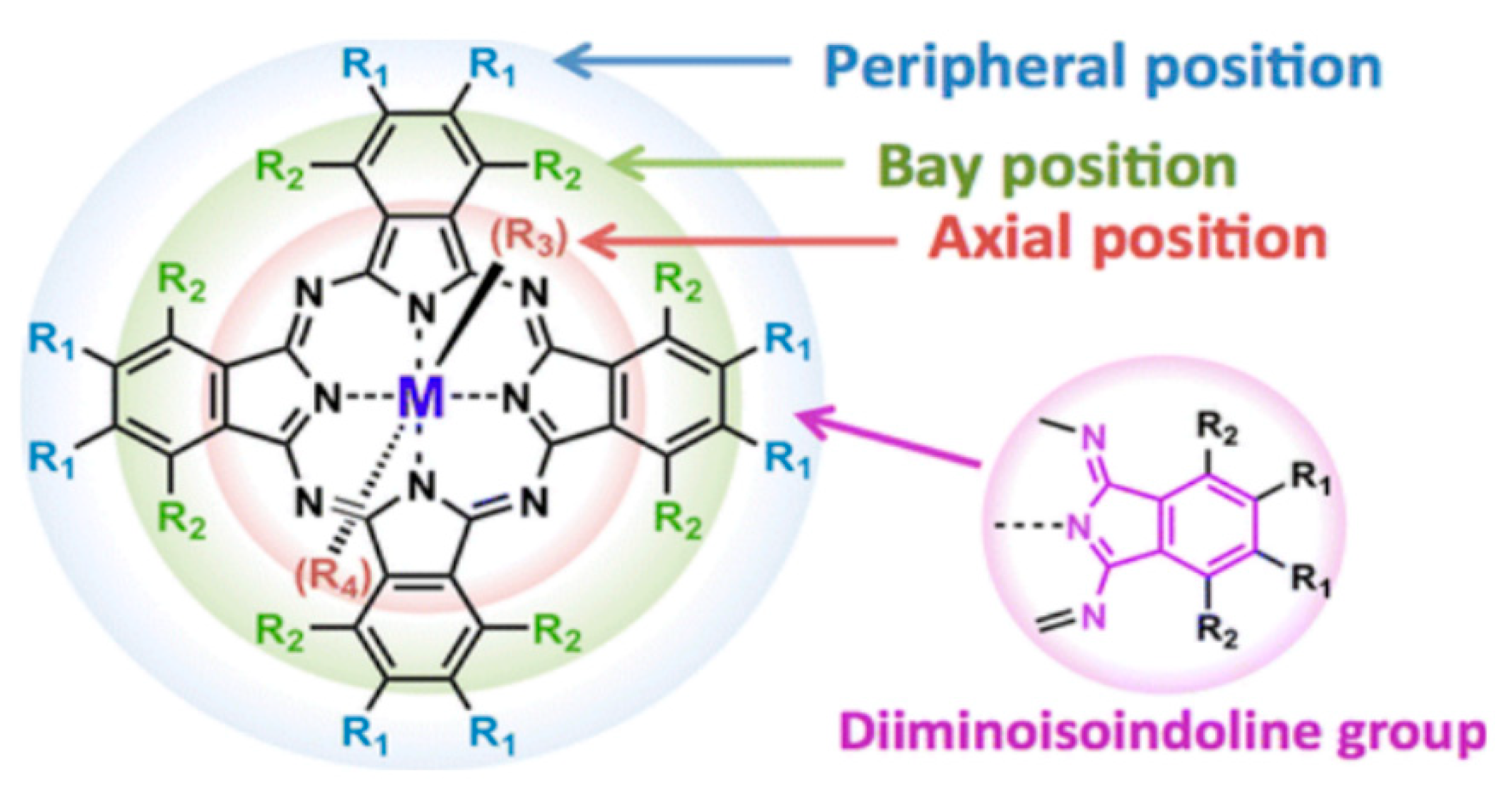
3. Phthalocyanines
4. Experimental Details
5. Results and Discussion
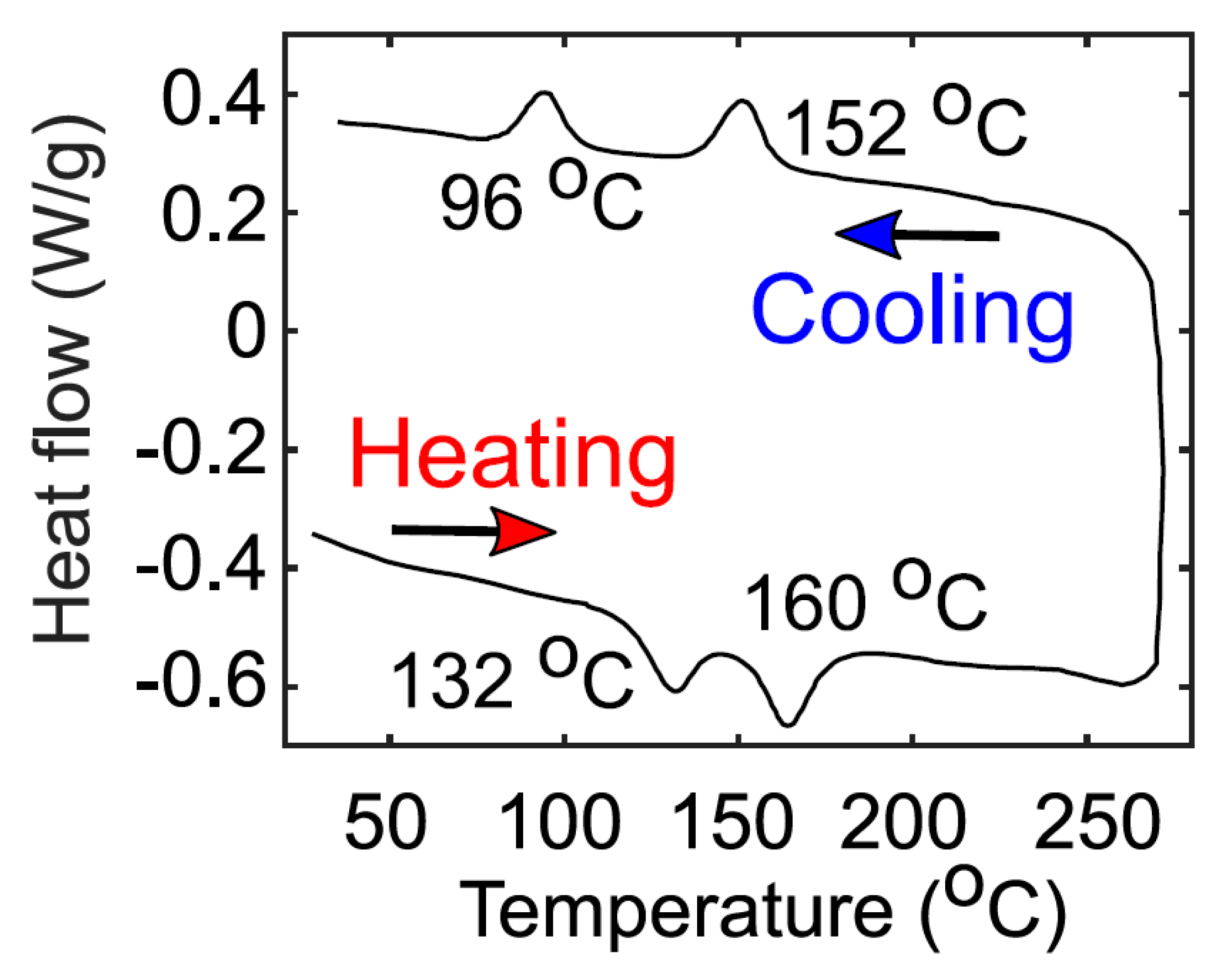
5.1. Differential Scanning Calorimetry (DSC)
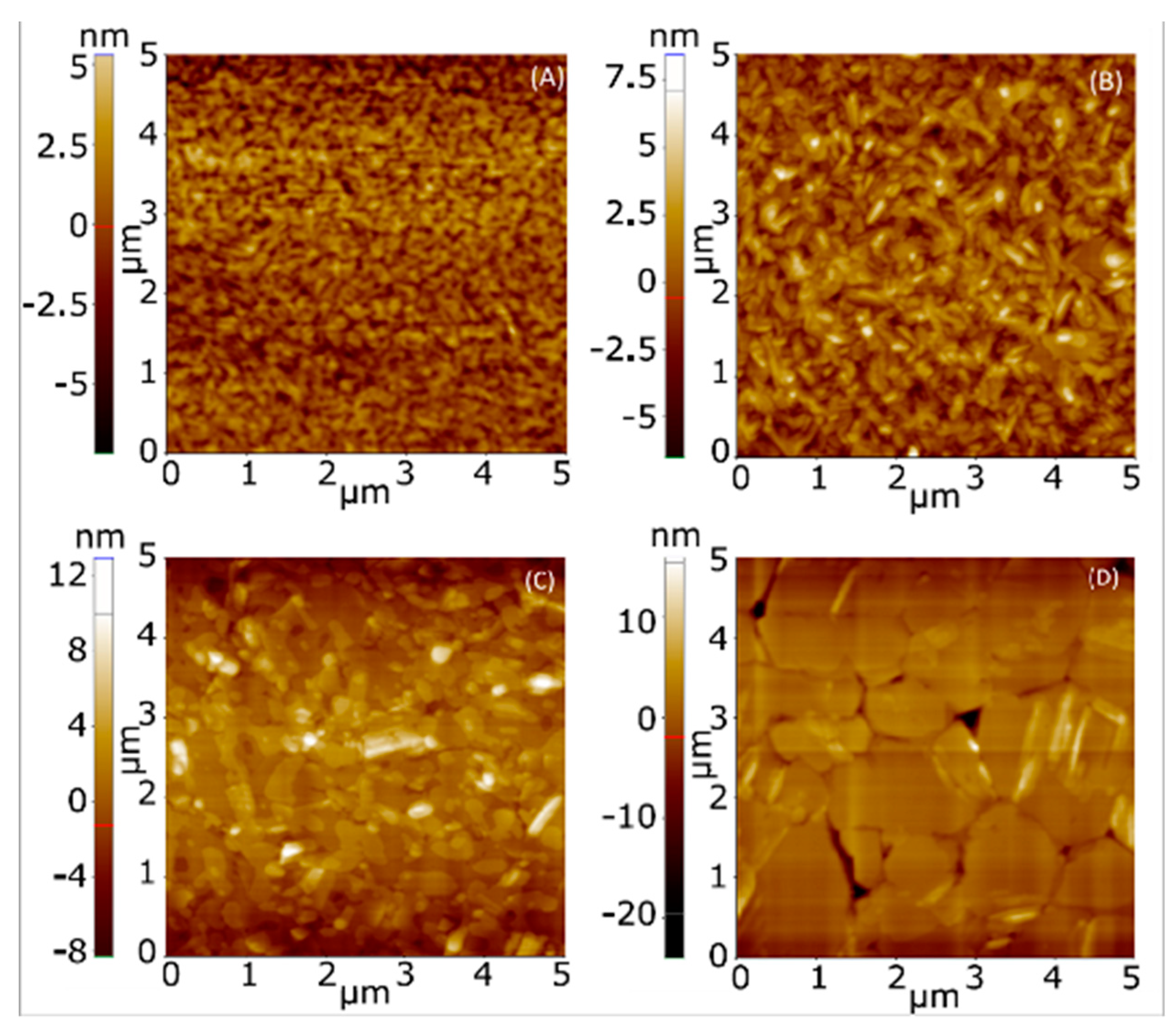
5.2. Atomic Force Microscope (AFM)
5.3. Electrical Behavior of -Based OTFTs
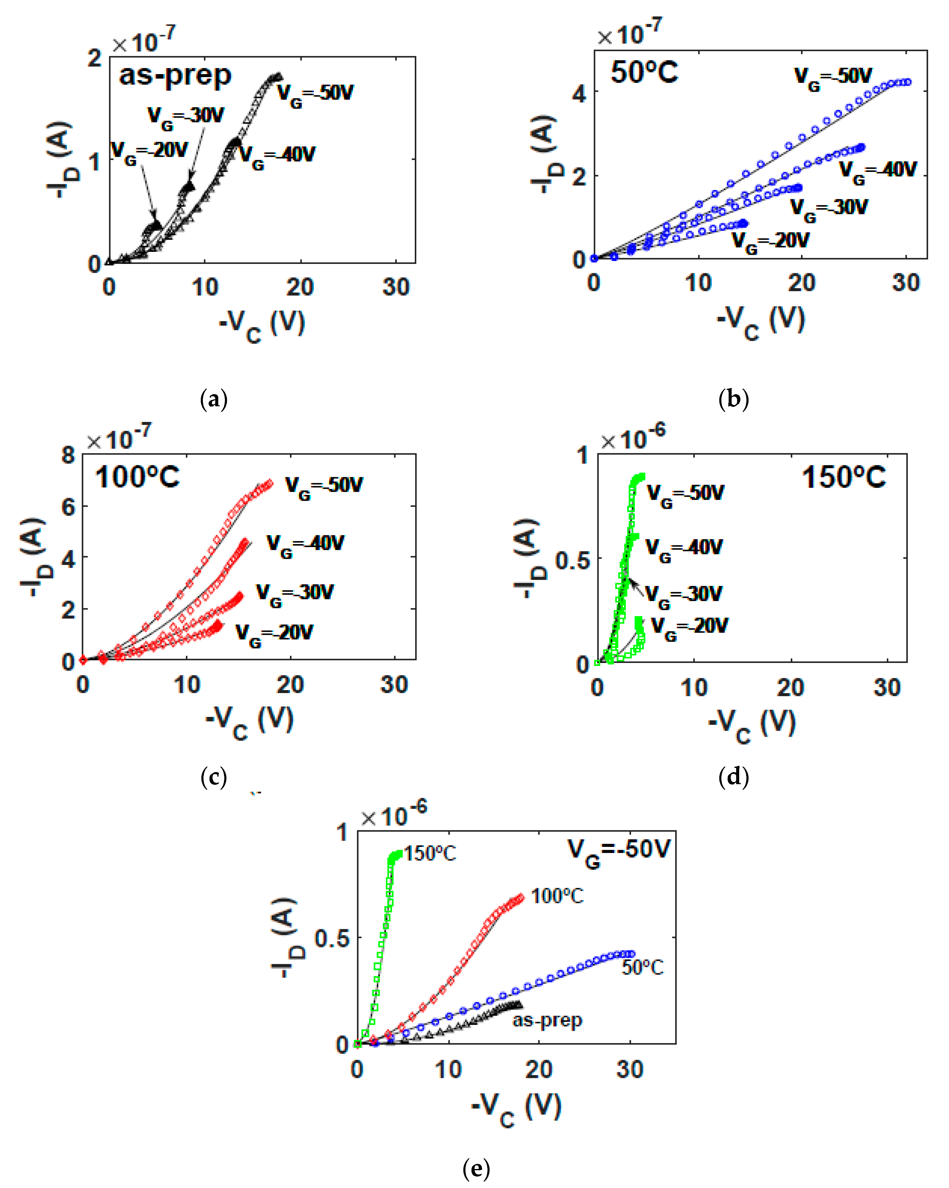
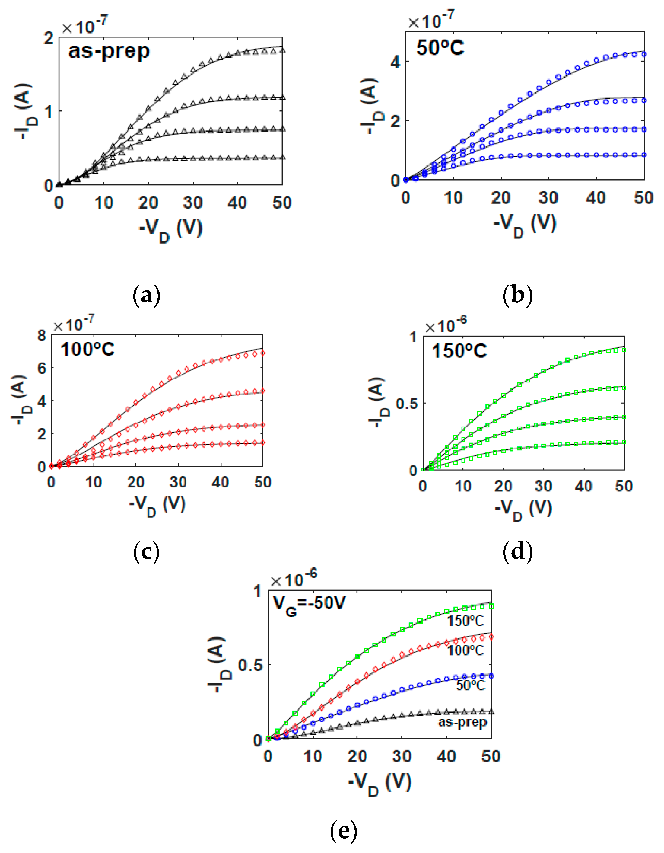
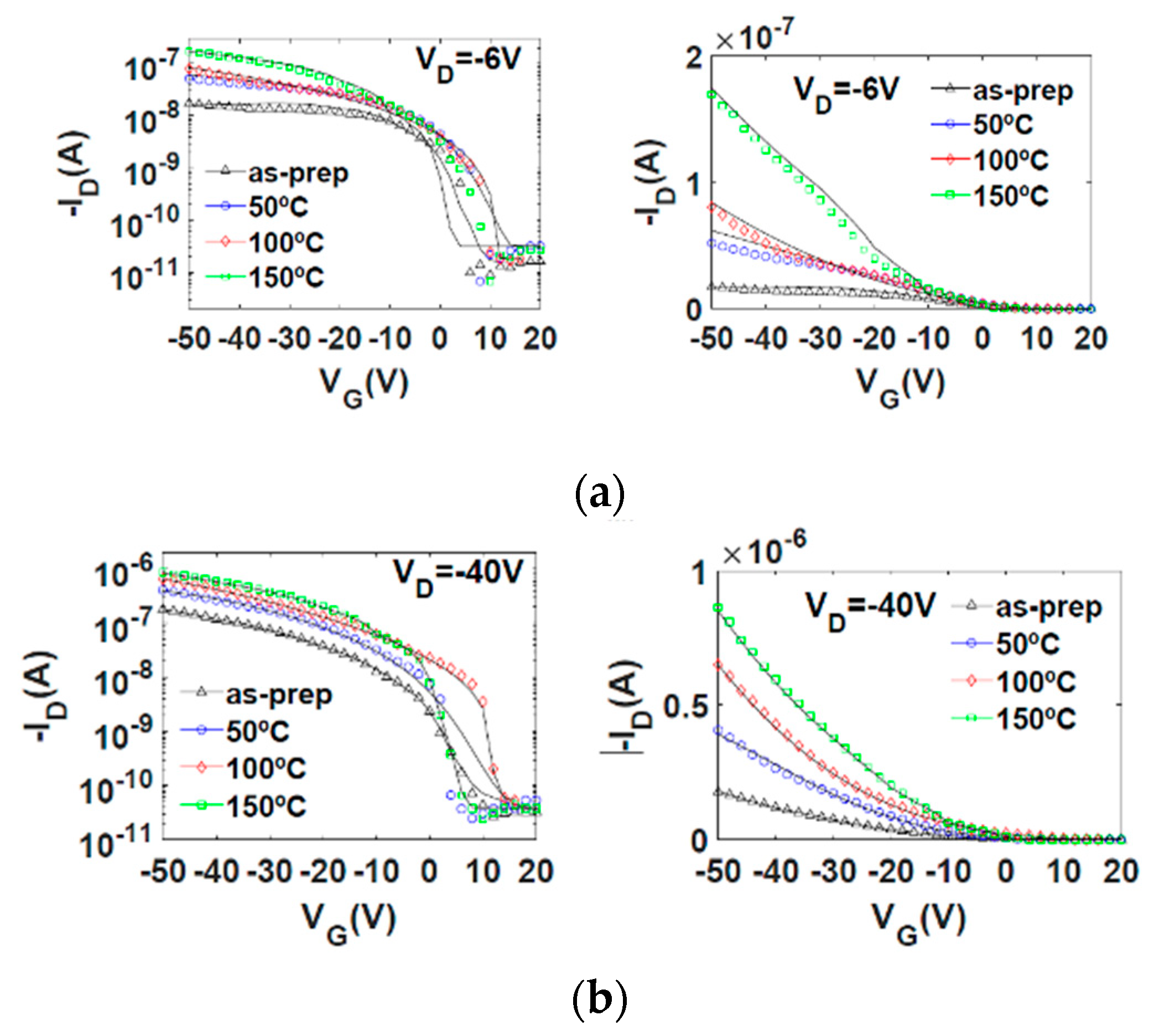
5.3.1. Current-Voltage Curves
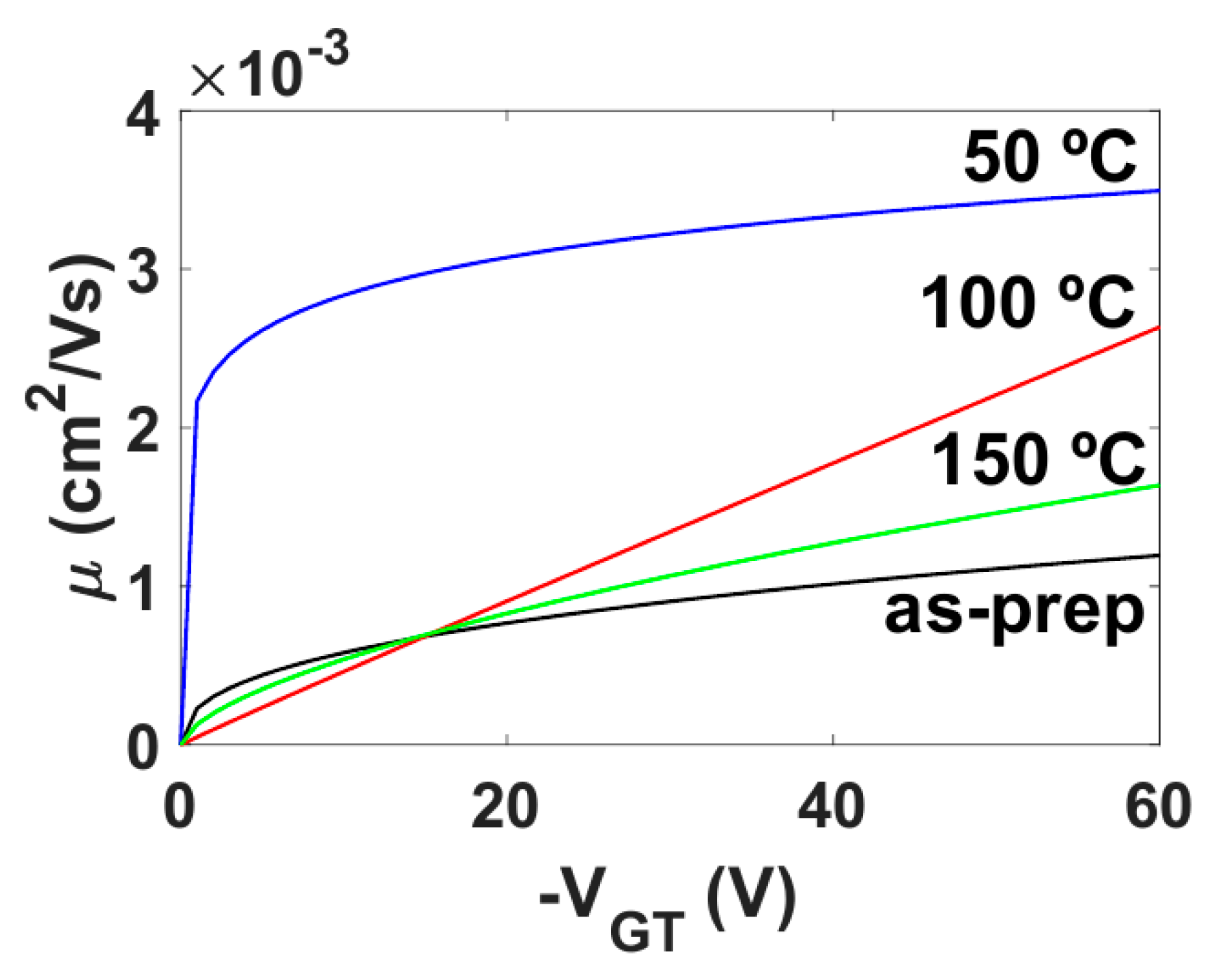
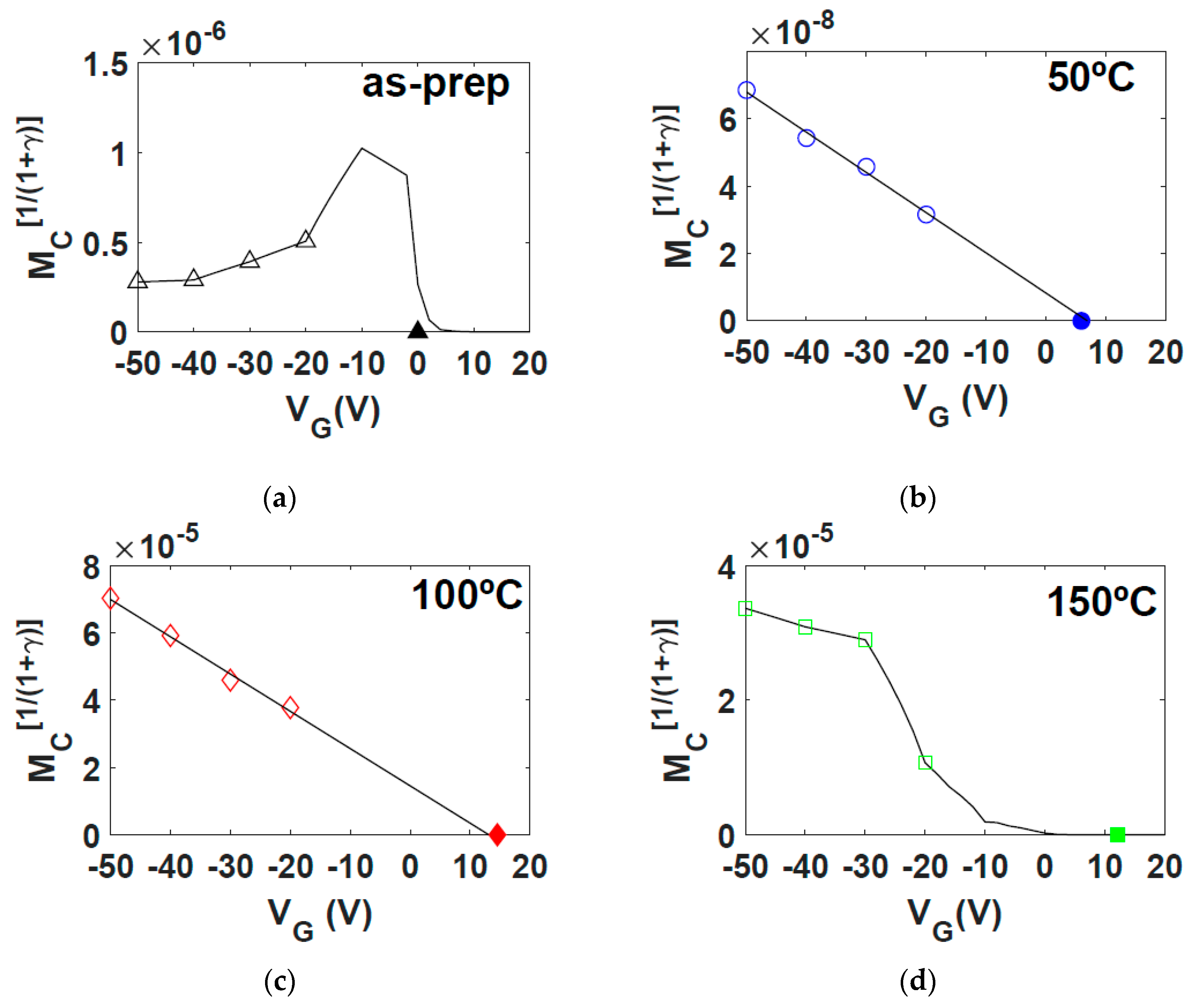
5.3.2. Evolution of OTFT Parameters with Annealing Temperature
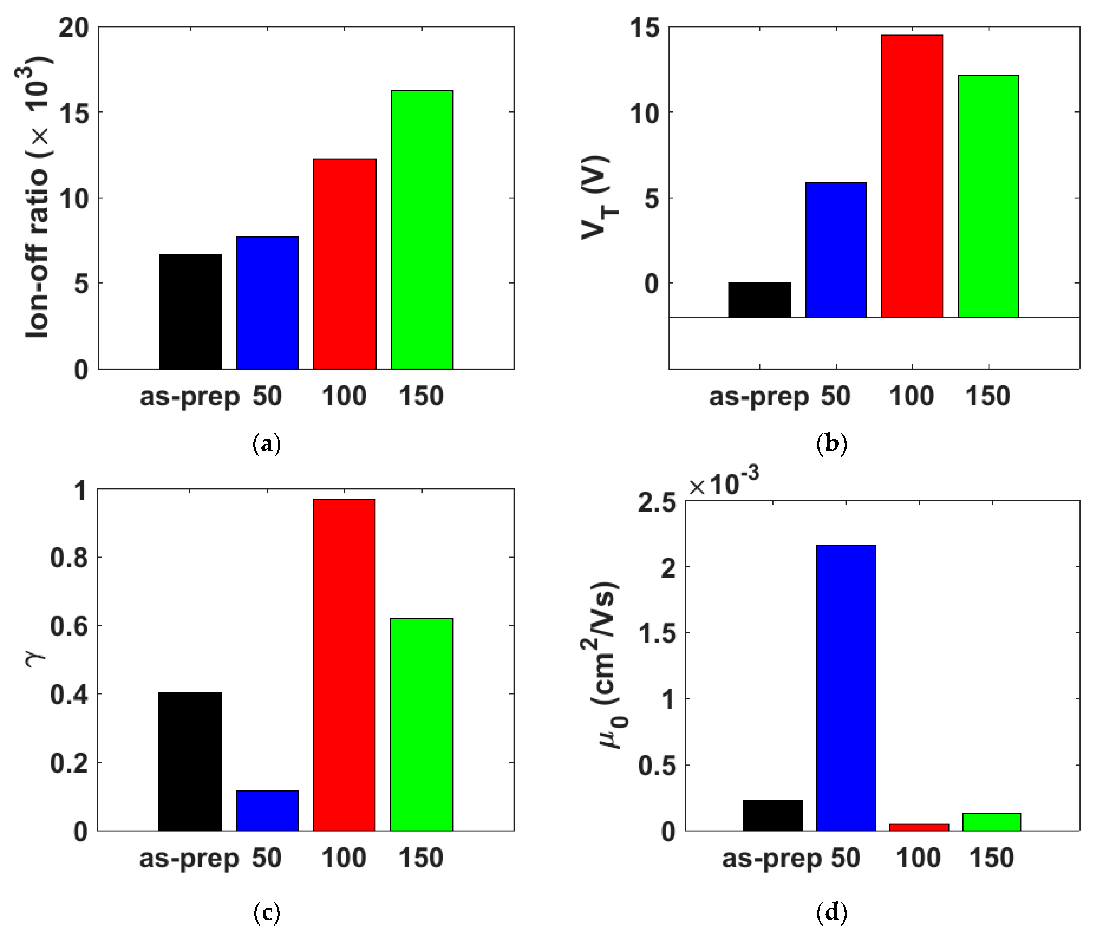
5.3.3. Discussions
6. Conclusions
Author Contributions
Funding
Acknowledgments
Conflicts of Interest
References
- Lamport, Z.A.; Haneef, H.F.; Anand, S.; Waldrip, M.; Jurchescu, O.D. Tutorial: Organic field-effect transistors: Materials, structure and operation. J. Appl. Phys. 2018, 124, 071101. [Google Scholar] [CrossRef]
- Guo, X.; Xu, Y.; Ogier, S.; Ng, T.N.; Caironi, M.; Perinot, A.; Li, L.; Zhao, J.; Tang, W.; Sporea, R.A.; et al. Current Status and Opportunities of Organic Thin-Film Transistor Technologies. IEEE Trans. Electron Device 2017, 64, 1906–1921. [Google Scholar] [CrossRef] [Green Version]
- Lee, C.J.; Chang, Y.C.; Wang, L.W.; Wang, Y.H. Biodegradable Materials for Organic Field-Effect Transistors on a Paper Substrate. IEEE Electron. Device Lett. 2019, 40, 236–239. [Google Scholar] [CrossRef]
- Masaya Kondo and Takafumi Uemura and Mihoko Akiyama and Naoko Namba and Masahiro Sugiyama and Yuki Noda and Teppei Araki and Shusuke Yoshimoto and Tsuyoshi Sekitani. Design of ultraflexible organic differential amplifier circuits for wearable sensor technologies. In Proceedings of the 2018 IEEE International Conference on Microelectronic Test Structures (ICMTS), Austin, TX, USA, 19–22 March 2018.
- Karimov, K.; Ahmed, M.M.; Noshin, F.; Saleem, M.; Mahroof-Tahir, M.; Moiz, S.A.; Akhmedov, K.M.; Zahid, M.; Abbas, S.Z.; Rashid, A. Nickel phthalocyanine based organic photo transistor: Effect of semiconductor film thickness. Eur. Phys. J. Appl. Phys. 2015, 72, 20202. [Google Scholar] [CrossRef]
- Liu, X.; Lin, Y.; Liao, Y.; Wu, J.; Zheng, Y. Recent advances in organic near-infrared photodiodes. J. Mater. Chem. C 2018, 6, 3499–3513. [Google Scholar] [CrossRef]
- Li, X.; Xiao, Y.; Wang, S.; Yang, Y.; Ma, Y.; Li, X. Polymorph-induced photosensitivity change in titanylphthalocyanine revealed by the charge transfer integral. Nanophotonics 2019, 8, 787–797. [Google Scholar] [CrossRef]
- Bohrer, F.I.; Colesniuc, C.N.; Park, J.; Ruidiaz, M.E.; Schuller, I.K.; Kummel, A.C.; Trogler, W.C. Comparative Gas Sensing in Cobalt, Nickel, Copper, Zinc, and Metal-Free Phthalocyanine Chemiresistors. JACS 2009, 131, 478–485. [Google Scholar] [CrossRef]
- Tomecek, D.; Hruska, M.; Fitl, P.; Vlcek, J.; Maresova, E.; Havlova, S.; Patrone, L.; Vrnata, M. Phthalocyanine Photoregeneration for Low Power Consumption Chemiresistors. ACS Sensors 2018, 3, 2558–2565. [Google Scholar] [CrossRef]
- Karimov, K.S.; Tahir, M.M.; Saleem, M.; Ahmad, R.T.M.; Abbas, S.Z. Nickel phthalocyanine based organic transistor. J. Optoelectron. Adv. Mater. 2017, 19, 347. [Google Scholar]
- Feng, X.; Shi, X.; Zhang, X.; Gu, W. Bottom-contact organic thin film transistors with transparent Ga-doped ZnO source-drain electrodes. Mater. Sci. Semicond. Proc. 2019, 101, 57–60. [Google Scholar] [CrossRef]
- Yuan, Y.; Giri, G.; Ayzner, A.L.; Zoombelt, A.P.; Mannsfeld, S.C.; Chen, J.; Nordlund, D.; Toney, M.F.; Huang, J.; Bao, Z. Ultra-high mobility transparent organic thin film transistors grown by an off-centre spin-coating method. Nat. Commun. 2014, 5, 1–9. [Google Scholar] [CrossRef] [PubMed]
- Xu, X.; Yao, Y.; Shan, B.; Gu, X.; Liu, D.; Liu, J.; Xu, J.; Zhao, N.; Hu, W.; Miao, Q. Electron Mobility Exceeding 10 cm2 V−1 s−1 and Band-Like Charge Transport in Solution-Processed n-Channel Organic Thin-Film Transistors. Adv. Mater. 2016, 28, 5276–5283. [Google Scholar] [CrossRef]
- Paterson, A.F.; Treat, N.D.; Zhang, W.; Fei, Z.; Wyatt-Moon, G.; Faber, H.; Vourlias, G.; Patsalas, P.A.; Solomeshch, O.; Tessler, N.; et al. Small Molecule/Polymer Blend Organic Transistors with Hole Mobility Exceeding 13 cm2/Vs. Adv. Mater. 2016, 28, 7791–7798. [Google Scholar] [CrossRef] [PubMed]
- He, D.; Qiao, J.; Zhang, L.; Wang, J.; Lan, T.; Qian, J.; Li, Y.; Shi, Y.; Chai, Y.; Lan, W.; et al. Ultrahigh mobility and efficient charge injection in monolayer organic thin-film transistors on boron nitride. Sci. Adv. 2017, 3, e1701186. [Google Scholar] [CrossRef] [PubMed]
- Rasheed, F.; Golanbari, M.S.; Marques, G.C.; Tahoori, M.B.; Aghassi-Hagmann, J. A Smooth EKV-Based DC Model for Accurate Simulation of Printed Transistors and Their Process Variations. IEEE Trans. Electron Device 2018, 65, 667–673. [Google Scholar] [CrossRef]
- Li, X.; Lee, G.S.; Park, S.H.; Kong, H.; An, T.K.; Kim, S.H. Direct writing of silver nanowire electrodes via dragging mode electrohydrodynamic jet printing for organic thin film transistors. Org. Electron. 2018, 62, 357–365. [Google Scholar] [CrossRef]
- Li, B.; Han, C.Y.; Lai, P.T.; Tang, W.M. Effects of source/drain-electrode material, thickness and fabrication method on the electrical performance of pentacene thin-film transistor. Thin Solid Films 2018, 667, 28–33. [Google Scholar] [CrossRef]
- Nair, S.; Kathiresan, M.; Mukundan, T. Two dimensional simulation of patternable conducting polymer electrode based organic thin film transistor. Semicond. Sci. Technol. 2018, 33, 025006. [Google Scholar] [CrossRef]
- Borthakur, T.; Sarma, R. Top-Contact Pentacene-Based Organic Thin Film Transistor (OTFT) with N,N′-Bis(3-Methyl Phenyl)-N,N′-Diphenyl Benzidine (TPD)/Au Bilayer Source-Drain Electrode. J. Electron. Mater. 2018, 47, 627–632. [Google Scholar] [CrossRef]
- Mei, Y.; Fogel, D.; Chen, J.; Ward, J.W.; Payne, M.M.; Anthony, J.E.; Jurchescu, O.D. Interface engineering to enhance charge injection and transport in solution-deposited organic transistors. Org. Electron. 2017, 50, 100–105. [Google Scholar] [CrossRef]
- Marinov, O.; Deen, M.J.; Zschieschang, U.; Klauk, H. Organic Thin-Film Transistors: Part I-Compact DC Modeling. IEEE Trans. Electron Device 2009, 56, 2952–2961. [Google Scholar] [CrossRef]
- Deen, M.J.; Marinov, O.; Zschieschang, U.; Klauk, H. Organic Thin-Film Transistors: Part II. Parameter Extraction. IEEE Trans. Electron Device 2009, 56, 2962–2968. [Google Scholar] [CrossRef]
- Kim, C.H.; Horowitz, G. Toward a Fully Analytical Contact Resistance Expression in Organic Transistors. Materials 2019, 12, 1169. [Google Scholar] [CrossRef] [PubMed]
- Estrada, M.; Cerdeira, A.; Puigdollers, J.; Resendiz, L.; Pallares, J.; Marsal, L.F.; Voz, C.; Iñiguez, B. Accurate modeling and parameter extraction method for organic TFTs. Solid State Electron. 2005, 49, 1009–1016. [Google Scholar] [CrossRef]
- Iñiguez, B.; Picos, R.; Veksler, D.; Koudymov, A.; Shur, M.S.; Ytterdal, T.; Jackson, W. Universal compact model for long- and short-channel Thin-Film Transistors. Solid State Electron. 2008, 52, 400–405. [Google Scholar] [CrossRef]
- Estrada, M.; Mejía, I.; Cerdeira, A.; Pallares, J.; Marsal, L.F.; Iñiguez, B. Mobility model for compact device modeling of OTFTs made with different materials. Solid State Electron. 2008, 52, 787–794. [Google Scholar] [CrossRef]
- Estrada, M.; Cerdeira, A.; Mejia, I.; Avila, M.; Picos, R.; Marsal, L.F.; Pallares, J.; Iñiguez, B. Modeling the behavior of charge carrier mobility with temperature in thin-film polymeric transistors. Microelectron. Eng. 2010, 87, 2565–2570. [Google Scholar] [CrossRef]
- Marinov, O.; Deen, M.J.; Iniguez, B. Charge transport in organic and polymer thin-film transistors: Recent issues. IEE Proc. Circ. Dev. Syst. 2005, 152, 189. [Google Scholar] [CrossRef]
- Kim, C.H.; Castro-Carranza, A.; Estrada, M.; Cerdeira, A.; Bonnassieux, Y.; Horowitz, G.; Iniguez, B. A Compact Model for Organic Field-Effect Transistors with Improved Output Asymptotic Behaviors. IEEE Trans. Electron Device 2013, 60, 1136–1141. [Google Scholar]
- Li, L.; Debucquoy, M.; Genoe, J.; Heremans, P. A compact model for polycrystalline pentacene thin-film transistor. J. Appl. Phys. 2010, 107, 024519. [Google Scholar] [CrossRef]
- Maiti, T.K.; Hayashi, T.; Chen, L.; Mori, H.; Kang, M.J.; Takimiya, K.; Miura-Mattausch, M.; Mattausch, H.J. A Surface Potential Based Organic Thin-Film Transistor Model for Circuit Simulation Verified with DNTT High Performance Test Devices. IEEE Trans. Semicond. Manuf. 2014, 27, 159–168. [Google Scholar] [CrossRef]
- Yaglioglu, B.; Agostinelli, T.; Cain, P.; Mijalković, S.; Nejim, A. Parameter Extraction and Evaluation of UOTFT Model for Organic Thin-Film Transistor Circuit Design. J. Disp. Technol. 2013, 9, 890–894. [Google Scholar] [CrossRef]
- Meixner, R.M.; Gobel, H.H.; Qiu, H.; Ucurum, C.; Klix, W.; Stenzel, R.; Yildirim, F.A.; Bauhofer, W.; Krautschneider, W.H. A Physical-Based PSPICE Compact Model for Poly(3-hexylthiophene) Organic Field-Effect Transistors. IEEE Trans. Electron Device 2008, 55, 1776–1781. [Google Scholar] [CrossRef] [Green Version]
- Fayez, M.; Morsi, K.M.; Sabry, M.N. OTFTs compact models: Analysis, comparison, and insights. IET Circ. Device Syst. 2017, 11, 409–420. [Google Scholar] [CrossRef]
- Fatima, S.; Rafique, U.; Ahmed, U.F.; Ahmed, M.M. A global parameters extraction technique to model organic field effect transistors output characteristics. Solid State Electron. 2019, 152, 81–92. [Google Scholar] [CrossRef]
- Romero, A.; González, J.; Picos, R.; Deen, M.J.; Jiménez-Tejada, J.A. Evolutionary parameter extraction for an organic TFT compact model including contact effects. Org. Electron. 2018, 61, 242–253. [Google Scholar] [CrossRef] [Green Version]
- Romero, A.; Jiménez, C.; González, J.; López-Varo, P.; Deen, M.J.; Jiménez-Tejada, J.A.A. Compact modeling of the effects of illumination on the contact region of organic phototransistors. Org. Electron. 2019, 70, 113–121. [Google Scholar] [CrossRef] [Green Version]
- Abdinia, S.; Torricelli, F.; Maiellaro, G.; Coppard, R.; Daami, A.; Jacob, S.; Mariucci, L.; Palmisano, G.; Ragonese, E.; Tramontana, F.; et al. Variation-based design of an AM demodulator in a printed complementary organic technology. Org. Electron. 2014, 15, 904–912. [Google Scholar] [CrossRef] [Green Version]
- Valletta, A.; Rapisarda, M.; Calvi, S.; Fortunato, G.; Frasca, M.; Maira, G.; Ciccazzo, A.; Mariucci, L. A DC and small signal AC model for organic thin film transistors including contact effects and non quasi static regime. Org. Electron. 2017, 41, 345–354. [Google Scholar] [CrossRef]
- Ma, A.M.; Barlage, D.W. Analysis of the Channel and Contact Regions in Staggered and Drain-Offset ZnO Thin-Film Transistors with Compact Modeling. IEEE Trans. Electron Device 2018, 65, 3277–3282. [Google Scholar] [CrossRef]
- Martins, R.; Gaspar, D.; Mendes, M.J.; Pereira, L.; Martins, J.; Bahubalindruni, P.; Barquinha, P.; Fortunato, E. Papertronics: Multigate paper transistor for multifunction applications. Appl. Mater. Today 2018, 12, 402–414. [Google Scholar] [CrossRef]
- Buonomo, M.; Lago, N.; Cantarella, G.; Wrachien, N.; Natali, M.; Prescimone, F.; Benvenuti, E.; Muccini, M.; Toffanin, S.; Cester, A. Simple and accurate single transistor technique for parameters extraction from organic and inorganic thin film devices. Org. Electron. 2018, 63, 376–383. [Google Scholar] [CrossRef]
- Li, L.; Gao, P.; Baumgarten, M.; Müllen, K.; Lu, N.; Fuchs, H.; Chi, L. High Performance Field-Effect Ammonia Sensors Based on a Structured Ultrathin Organic Semiconductor Film. Adv. Mater. 2013, 25, 3419–3425. [Google Scholar] [CrossRef] [PubMed]
- Ren, X.; Pei, K.; Peng, B.; Zhang, Z.; Wang, Z.; Wang, X.; Chan, P.K. A Low-Operating-Power and Flexible Active-Matrix Organic-Transistor Temperature-Sensor Array. Adv. Mater. 2016, 28, 4832–4838. [Google Scholar] [CrossRef] [PubMed]
- Wang, Z.; Guo, S.; Li, H.; Wang, B.; Sun, Y.; Xu, Z.; Chen, X.; Wu, K.; Zhang, X.; Xing, F.; et al. The Semiconductor/Conductor Interface Piezoresistive Effect in an Organic Transistor for Highly Sensitive Pressure Sensors. Adv. Mater. 2018, 31, 1805630. [Google Scholar] [CrossRef] [PubMed]
- Romero, A.; González, J.; Deen, M.J.; Jiménez-Tejada, J.A. Versatile Model for the Contact Region of Organic Thin-Film Transistors. Org. Electron. 2019. in Manuscript Submitted for Publication. [Google Scholar]
- Marinov, O.; Deen, M.J.; Datars, R. Compact modeling of charge carrier mobility in organic thin-film transistors. J. Appl. Phys. 2009, 106, 064501. [Google Scholar] [CrossRef]
- Bürgi, L.; Sirringhaus, H.; Friend, R.H. Noncontact potentiometry of polymer field-effect transistors. Appl. Phys. Lett. 2002, 80, 2913–2915. [Google Scholar] [CrossRef]
- Jiménez-Tejada, J.A.; López-Villanueva, J.A.; López-Varo, P.; Awawdeh, K.M.; Deen, M.J. Compact modeling and contact effects in organic transistors. IEEE Trans. Electron Device 2014, 61, 266–277. [Google Scholar] [CrossRef]
- Valletta, A.; Daami, A.; Benwadih, M.; Coppard, R.; Fortunato, G.; Rapisarda, M.; Torricelli, F.; Mariucci, L. Contact effects in high performance fully printed p-channel organic thin film transistors. Appl. Phys. Lett. 2011, 99, 233309. [Google Scholar] [CrossRef] [Green Version]
- Mariucci, L.; Rapisarda, M.; Valletta, A.; Jacob, S.; Benwadih, M.; Fortunato, G. Current spreading effects in fully printed p-channel organic thin film transistors with Schottky source-drain contacts. Org. Electron. 2013, 14, 86–93. [Google Scholar] [CrossRef]
- Charbonneau, M.; Locatelli, D.; Lombard, S.; Serbutoviez, C.; Tournon, L.; Torricelli, F.; Abdinia, S.; Cantatore, E.; Fattori, M. A Large-Area Gravure Printed Process for P-type Organic Thin-Film Transistors on Plastic Substrates. In Proceedings of the 2018 48th European Solid-State Device Research Conference (ESSDERC), Dresden, Germany, 3–6 September 2018. [Google Scholar]
- Gundlach, D.J.; Zhou, L.; Nichols, J.A.; Jackson, T.N.; Necliudov, P.V.; Shur, M.S. An experimental study of contact effects in organic thin film transistors. J. Appl. Phys. 2006, 100, 024509. [Google Scholar] [CrossRef]
- Jiménez-Tejada, J.A.; Awawdeh, K.M.; López-Villanueva, J.A.; Carceller, J.E.; Deen, M.J.; Chaure, N.B.; Basova, T.; Ray, A.K. Contact effects in compact models of organic thin film transistors: Application to zinc phthalocyanine-based transistors. Org. Electron. 2011, 12, 832–842. [Google Scholar] [CrossRef]
- Deen, M.J.; Kazemeini, M.H.; Holdcroft, S. Contact effects and extraction of intrinsic parameters in poly(3-alkylthiophene) thin film field-effect transistors. J. Appl. Phys. 2008, 103, 124509. [Google Scholar] [CrossRef]
- Rajeev, V.R.; Paulose, A.K.; Unni, K.N. Ammonia gas detection using field-effect transistor based on a solution-processable organic semiconductor. Vacuum 2018, 158, 271–277. [Google Scholar] [CrossRef]
- Lara Bullejos, P.; Jiménez Tejada, J.A.; Deen, M.J.; Marinov, O.; Datars, W.R. Unified model for the injection and transport of charge in organic diodes. J. Appl. Phys. 2008, 103, 064504. [Google Scholar] [CrossRef]
- Lara Bullejos, P.; Jimenez Tejada, J.A.; Rodriguez-Bolivar, S.; Deen, M.J.; Marinov, O. Model for the injection of charge through the contacts of organic transistors. J. Appl. Phys. 2009, 105, 084516. [Google Scholar] [CrossRef]
- Lara Bullejos, P.; Jiménez-Tejada, J.A.; Gómez-Campos, F.M.; Deen, M.J.; Marinov, O. Evaluation of the charge density in the contact region of organic thin film transistors. J. Appl. Phys. 2009, 106, 094503. [Google Scholar] [CrossRef]
- López-Varo, P.; Jiménez-Tejada, J.A.; López-Villanueva, J.A.; Carceller, J.E.; Deen, M.J. Modeling the transition from ohmic to space charge limited current in organic semiconductors. Org. Electron. 2012, 13, 1700–1709. [Google Scholar] [CrossRef]
- Jiménez-Tejada, J.A.; López-Varo, P.; Cammidge, A.N.; Chambrier, I.; Cook, M.J.; Chaure, N.B.; Ray, A.K. Compact Modeling of Organic Thin-Film Transistors with Solution Processed Octadecyl Substituted Tetrabenzotriazaporphyrin as an Active Layer. IEEE Trans. Electron Device 2017, 64, 2629–2634. [Google Scholar] [CrossRef] [Green Version]
- Jiménez Tejada, J.A.; Lopez-Varo, P.; Chaure, N.B.; Chambrier, I.; Cammidge, A.N.; Cook, M.J.; Jafari-Fini, A.; Ray, A.K. Organic thin film transistors using a liquid crystalline palladium phthalocyanine as active layer. J. Appl. Phys. 2018, 123, 115501. [Google Scholar] [CrossRef] [Green Version]
- Awawdeh, K.M.; Jiménez-Tejada, J.A.; López Varo, P.; López Villanueva, J.A.; Gómez Campos, F.M.; Deen, M.J. Characterization of organic thin film transistors with hysteresis and contact effects. Org. Electron. 2013, 14, 3286–3296. [Google Scholar] [CrossRef]
- Gruber, M.; Zojer, E.; Schürrer, F.; Zojer, K. Impact of Materials versus Geometric Parameters on the Contact Resistance in Organic Thin-Film Transistors. Adv. Funct. Mater. 2013, 23, 2941–2952. [Google Scholar] [CrossRef]
- Sohn, C.W.; Rim, T.U.; Choi, G.B.; Jeong, Y.H. Analysis of contact effects in inverted-staggered organic thin-film transistors based on anisotropic conduction. IEEE Trans. Electron Device 2010, 57, 986–994. [Google Scholar] [CrossRef]
- Borchert, J.W.; Peng, B.; Letzkus, F.; Burghartz, J.N.; Chan, P.K.L.; Zojer, K.; Ludwigs, S.; Klauk, H. Small contact resistance and high frequency operation of flexible low-voltage inverted coplanar organic transistors. Nat. Commun. 2019, 10, 1119. [Google Scholar] [CrossRef] [PubMed]
- Harper, A.F.; Diemer, P.J.; Jurchescu, O.D. Contact patterning by laser printing for flexible electronics on paper. npj Flex. Electron. 2019, 3, 11. [Google Scholar] [CrossRef]
- Deen, M.J.; Kazemeini, M.H. Photosensitive polymer thin-film FETs based on poly (3-octylthiophene). Proc. IEEE 2005, 93, 1312–1320. [Google Scholar] [CrossRef]
- Takanashi, Y.; Takahata, K.; Muramoto, Y. Characteristics of InAlAs/InGaAs high electron mobility transistors under 1.3-μm laser illumination. IEEE Electron Device Lett. 1998, 19, 472–474. [Google Scholar] [CrossRef]
- Takanashi, Y.; Takahata, K.; Muramoto, Y. Characteristics of InAlAs/InGaAs high-electron-mobility transistors under illumination with modulated light. IEEE Trans. Electron Device 1999, 46, 2271–2277. [Google Scholar] [CrossRef]
- Sze, S.M.; Ng, K.K. Physics of Semiconductor Devices; John Wiley & Sons: Hoboken, NJ, USA, 2006. [Google Scholar]
- Kang, H.S.; Choi, C.S.; Choi, W.Y.; Kim, D.H.; Seo, K.S. Characterization of phototransistor internal gain in metamorphic high-electron-mobility transistors. Appl. Phys. Lett. 2004, 84, 3780–3782. [Google Scholar] [CrossRef] [Green Version]
- Sangeeth, C.S.; Stadler, P.; Schaur, S.; Sariciftci, N.S.; Menon, R. Interfaces and traps in pentacene field-effect transistor. J. Appl. Phys. 2010, 108, 113703. [Google Scholar] [CrossRef]
- Peng, Y.; Lv, W.; Yao, B.; Fan, G.; Chen, D.; Gao, P.; Zhou, M.; Wang, Y. High performance near infrared photosensitive organic field-effect transistors realized by an organic hybrid planar-bulk heterojunction. Org. Electron. 2013, 14, 1045–1051. [Google Scholar] [CrossRef]
- Boukhili, W.; Tozlu, C.; Mahdouani, M.; Erten-Ela, S.; Bourguiga, R. Illumination and dipole layer effects on the density of state distribution in n-type organic thin film phototransistors based on naphthalene bis-benzimidazole: Experiment and modeling. Microelectron. Eng. 2017, 179, 37–47. [Google Scholar] [CrossRef]
- Cerdeira, A.; Estrada, M.; Garcıa, R.; Ortiz-Conde, A.; Sánchez, F.G. New procedure for the extraction of basic a-Si:H TFT model parameters in the linear and saturation regions. Solid State Electron. 2001, 45, 1077–1080. [Google Scholar] [CrossRef]
- Marinov, O.; Jamal Deen, M.; Feng, C.; Wu, Y. Precise parameter extraction technique for organic thin-film transistors operating in the linear regime. J. Appl. Phys. 2014, 115, 034506. [Google Scholar] [CrossRef]
- Berger, H.H. Contact resistance and contact resistivity. J. Electrochem. Soc. 1972, 119, 507–514. [Google Scholar] [CrossRef]
- Kraft, U.; Anthony, J.E.; Ripaud, E.; Loth, M.A.; Weber, E.; Klauk, H. Low-Voltage Organic Transistors Based on Tetraceno[2,3-b]thiophene: Contact Resistance and Air Stability. Chem. Mater. 2015, 27, 998–1004. [Google Scholar] [CrossRef]
- Hamadani, B.H.; Natelson, D. Nonlinear charge injection in organic field-effect transistors. J. Appl. Phys. 2005, 97, 064508. [Google Scholar] [CrossRef] [Green Version]
- Krammer, M.; Borchert, J.W.; Petritz, A.; Karner-Petritz, E.; Schider, G.; Stadlober, B.; Klauk, H.; Zojer, K. Critical Evaluation of Organic Thin-Film Transistor Models. Crystals 2019, 9, 85. [Google Scholar] [CrossRef]
- Romero, A.; González, J.; Jiménez-Tejada, J.A. Constrained Many-Objective Evolutionary Extraction Procedure for an OTFT Compact Model Including Contact Effects. In Proceedings of the 2018 Spanish Conference on Electron Devices (CDE), Salamanca, Spain, 14–16 November 2018; pp. 1–4. [Google Scholar]
- Sean Luke. ECJ Evolutionary Computation Library. 1998. Available online: https://cs.gmu.edu/~eclab/projects/ecj/ (accessed on 8 August 2019).
- González, J.; Rojas, I.; Ortega, J.; Pomares, H.; Fernandez, F.J.; Díaz, A.F. Multiobjective evolutionary optimization of the size, shape, and position parameters of radial basis function networks for function approximation. IEEE Trans. Neural Netw. 2003, 14, 1478–1495. [Google Scholar] [CrossRef]
- Gsänger, M.; Bialas, D.; Huang, L.; Stolte, M.; Würthner, F. Organic Semiconductors based on Dyes and Color Pigments. Adv. Mater. 2016, 28, 3615–3645. [Google Scholar] [CrossRef] [PubMed]
- Zhang, Y.; Cai, X.; Bian, Y.; Jiang, J. Organic Semiconductors of Phthalocyanine Compounds for Field Effect Transistors (FETs); Springer: Berlin/Heidelberg, Germany, 2010; pp. 275–321. [Google Scholar]
- Melville, O.A.; Lessard, B.H.; Bender, T.P. Phthalocyanine-Based Organic Thin-Film Transistors: A Review of Recent Advances. ACS Appl. Mater. Interfaces 2015, 7, 13105–13118. [Google Scholar] [CrossRef] [PubMed]
- Bao, Z.; Lovinger, A.J.; Dodabalapur, A. Highly ordered vacuum-deposited thin films of metallophthalocyanines and their applications in Field-effect transistors. Adv. Mater. 1997, 9, 42–44. [Google Scholar] [CrossRef]
- Karimov, K.H.S.; Saleem, M.; Ahmed, N.; Tahir, M.M.; Zahid, M.S.; Sajid, M.; Bashir, M.M. Effect of humidity on the NiPc based organic photo field effect transistor. Proc. Rom. Acad. Ser. A Math. Phys. 2016, 17, 84–89. [Google Scholar]
- Fatima, N.; Ahmed, M.M.; Karimov, K.S.; Ahmedov, K. Humidity effect on organic semiconductor NiPc films deposited at different gravity conditions. IOP Conf. Ser. Mater. Sci. Eng. 2016, 146, 012035. [Google Scholar] [CrossRef] [Green Version]
- Qiu, C.J.; Dou, Y.W.; Qu, W.; Sun, Y.M. Nitrogen dioxide sensing properties and mechanism of nickel phthalocyanine film. Proc. SPIE 2009, 7493, 749366. [Google Scholar]
- Muzikante, I.; Parra, V.; Dobulans, R.; Fonavs, E.; Latvels, J.; Bouvet, M. A novel gas sensor transducer based on phthalocyanine heterojunction devices. Sensors 2007, 7, 2984–2996. [Google Scholar] [CrossRef] [PubMed]
- Ishimaru, Y.; Wada, M.; Fukuda, T.; Kamata, N. Red-Sensitive Organic Photoconductive Device Using Soluble Ni-Phthalocyanine. IEICE Trans. Electron. 2011, E94.C, 187–189. [Google Scholar] [CrossRef]
- Haider, M.; Zhen, C.; Wu, T.; Liu, G.; Cheng, H.M. Boosting efficiency and stability of perovskite solar cells with nickel phthalocyanine as a low-cost hole transporting layer material. J. Mater. Sci. Technol. 2018, 34, 1474–1480. [Google Scholar] [CrossRef]
- Haider, M.; Zhen, C.; Wu, T.; Wu, J.; Jia, C.; Liu, G.; Cheng, H.M. Nickel phthalocyanine as an excellent hole-transport material in inverted planar perovskite solar cells. Chem. Commun. 2019, 55, 5343–5346. [Google Scholar] [CrossRef]
- Madhuri, K.P.; John, N.S. Supercapacitor application of nickel phthalocyanine nanofibres and its composite with reduced graphene oxide. Appl. Surf. Sci. 2018, 449, 528–536. [Google Scholar] [CrossRef]
- Madhuri, K.P.; John, N.S. Metallophthalocyanine-nanofibre-based electrodes for electrochemical sensing of biomolecules. Bull. Mater. Sci. 2018, 41, 118. [Google Scholar] [CrossRef] [Green Version]
- Jia, H.; Yao, Y.; Zhao, J.; Gao, Y.; Luo, Z.; Du, P. A novel two-dimensional nickel phthalocyanine-based metal-organic framework for highly efficient water oxidation catalysis. J. Mater. Chem. A 2018, 6, 1188–1195. [Google Scholar] [CrossRef]
- Hong, J.Y.; Fauvell, T.J.; Helweh, W.; Zhang, X.Y.; Chen, L.X. Investigation of the photoinduced axial ligation process in the excited state of nickel(II) phthalocyanine. J. Photochem. Photobiol. A Chem. 2019, 372, 270–278. [Google Scholar] [CrossRef]
- Boileau, N.T.; Cranston, R.; Mirka, B.; Melville, O.A.; Lessard, B.H. Metal phthalocyanine organic thin-film transistors: Changes in electrical performance and stability in response to temperature and environment. RSC Adv. 2019, 9, 21478–21485. [Google Scholar] [CrossRef]
- Chaure, N.B.; Cammidge, A.N.; Chambrier, I.; Cook, M.J.; Ray, A.K. A Tetrabenzotriazaporphyrin Based Organic Thin Film Transistor: Comparison with a Device of the Phthalocyanine Analogue. ECS J. Solid State Sci. Technol. 2015, 4, P3086–P3090. [Google Scholar] [CrossRef] [Green Version]
- Basova, T.V.; Durmus, M.; Guerek, A.G.; Ahsen, V.; Hassan, A. Effect of Interface on the Orientation of the Liquid Crystalline Nickel Phthalocyanine Films. J. Phys. Chem. C 2009, 113, 19251–19257. [Google Scholar] [CrossRef]
- Chaidogiannos, G.; Petraki, F.; Glezos, N.; Kennou, S.; Nespurek, S. Low voltage operating OFETs based on solution processed metal phthalocyanines. Appl. Phys. A Mater. Sci. Process. 2009, 96, 763–767. [Google Scholar] [CrossRef]
- Basova, T.V.; Hassan, A.; Durmus, M.; Gurek, A.G.; Ahsen, V. Orientation of the liquid crystalline nickel phthalocyanine films confined between electrodes. Synth. Met. 2011, 161, 1996–2000. [Google Scholar] [CrossRef]
- Basova, T.V.; Parkhomenko, R.G.; Igumenov, I.K.; Hassan, A.; Durmus, M.; Gurek, A.G.; Ahsen, V. Composites of liquid crystalline nickel phthalocyanine with gold nanoparticles: Liquid crystalline behaviour and optical properties. Dyes Pigm. 2014, 111, 58–63. [Google Scholar] [CrossRef]
- Basova, T.; Hassan, A.; Durmuſ, M.; Gürek, A.G.; Ahsen, V. Liquid crystalline metal phthalocyanines: Structural organization on the substrate surface. Coord. Chem. Rev. 2016, 310, 131–153. [Google Scholar] [CrossRef]
- Chaure, N.B.; Cammidge, A.N.; Chambrier, I.; Cook, M.J.; Cain, M.G.; Murphy, C.E.; Pal, C.; Ray, A.K. High-mobility solution-processed copper phthalocyanine-based organic field-effect transistors. Sci. Technol. Adv. Mater. 2011, 12, 025001. [Google Scholar] [CrossRef] [PubMed]
- Cherodian, A.S.; Davies, A.N.; Richardson, R.M.; Cook, M.J.; McKeown, N.B.; Thomson, A.J.; Feijoo, J.; Ungar, G.; Harrison, J. Mesogenic Behaviour of some 1,4,8,11,15,18,22,25-Octa-alkylphthalocyanines. Mol. Cryst. Liq. Cryst. 1991, 196, 103–114. [Google Scholar] [CrossRef]


| Parameter | Samples (Annealing Temperature, °C) | Extracted From | |||
|---|---|---|---|---|---|
| As-Prepared | 50 | 100 | 150 | ||
| Average particle size (μm) | 100 ± 10 | 200 ± 20 | 400 ± 20 | 1500 ± 100 | AFM data |
| Surface roughness (nm) | 1.52 | 17.80 | 42.62 | 65.19 | AFM data |
| μ0 (cm2/Vs) | 2.30 × 10⁻⁴ | 2.16 × 10⁻³ | 4.93 × 10⁻⁵ | 1.29 × 10⁻⁴ | (5), (18), (20) |
| γ | 0.402 | 0.116 | 0.971 | 0.619 | (5), (18), (20) |
| (V) | 4.18 × 10⁻⁷ | 5.90 | 14.5 | 12.1 | (5), (18), (20) |
| (V) | - | 6.91 | 13.1 | - | (10) |
| α [A/V(mk+1+γ] | - | 1.08 × 10⁻¹⁰ | 1.81 × 10⁻¹² | - | (10) |
| VSS (V) | −8.88 | −3.41 | −20.4 | −21.2 | (5), (18), (20) |
| mk | 1.98 | 1.10 | 1.64 | 2.00 | (5), (18), (20) |
| MC(−20 V) [A/Vmk] | 1.48 × 10⁻⁹ | 4.21 × 10⁻⁹ | 1.90 × 10⁻⁹ | 8.91 × 10⁻⁹ | (5), (18), (20) |
| MC(−30 V) [A/Vmk] | 1.04 × 10⁻⁹ | 6.38 × 10⁻⁹ | 2.80 × 10⁻⁹ | 4.47 × 10⁻⁸ | (5), (18), (20) |
| MC(−40 V) [A/Vmk] | 6.82 × 10⁻¹⁰ | 7.72 × 10⁻⁹ | 4.62 × 10⁻⁹ | 4.96 × 10⁻⁸ | (5), (18), (20) |
| MC(−50 V) [A/Vmk] | 6.46 × 10⁻¹⁰ | 1.00 × 10⁻⁸ | 6.48 × 10⁻⁹ | 5.70 × 10⁻⁸ | (5), (18), (20) |
© 2019 by the authors. Licensee MDPI, Basel, Switzerland. This article is an open access article distributed under the terms and conditions of the Creative Commons Attribution (CC BY) license (http://creativecommons.org/licenses/by/4.0/).
Share and Cite
Jiménez-Tejada, J.A.; Romero, A.; González, J.; Chaure, N.B.; Cammidge, A.N.; Chambrier, I.; Ray, A.K.; Deen, M.J. Evolutionary Computation for Parameter Extraction of Organic Thin-Film Transistors Using Newly Synthesized Liquid Crystalline Nickel Phthalocyanine. Micromachines 2019, 10, 683. https://doi.org/10.3390/mi10100683
Jiménez-Tejada JA, Romero A, González J, Chaure NB, Cammidge AN, Chambrier I, Ray AK, Deen MJ. Evolutionary Computation for Parameter Extraction of Organic Thin-Film Transistors Using Newly Synthesized Liquid Crystalline Nickel Phthalocyanine. Micromachines. 2019; 10(10):683. https://doi.org/10.3390/mi10100683
Chicago/Turabian StyleJiménez-Tejada, Juan A., Adrián Romero, Jesús González, Nandu B. Chaure, Andrew N. Cammidge, Isabelle Chambrier, Asim K. Ray, and M. Jamal Deen. 2019. "Evolutionary Computation for Parameter Extraction of Organic Thin-Film Transistors Using Newly Synthesized Liquid Crystalline Nickel Phthalocyanine" Micromachines 10, no. 10: 683. https://doi.org/10.3390/mi10100683