Si-Based Materials for Thermoelectric Applications


1
Graduate School of Engineering, Osaka University, 2-1 Yamadaoka, Suita, Osaka 565-0871, Japan
2
Institute for Integrated Radiation and Nuclear Science, Kyoto University, 2 Asashiro-Nishi, Kumatori-cho, Sennan-gun, Osaka 590-0494, Japan
3
Research Institute of Nuclear Engineering, University of Fukui, 1-3-33 Kanawa-cho, Tsuruga, Fukui 914-0055, Japan
*
Authors to whom correspondence should be addressed.
Materials 2019, 12(12), 1943; https://doi.org/10.3390/ma12121943
Submission received: 21 May 2019
/
Revised: 13 June 2019
/
Accepted: 14 June 2019
/
Published: 17 June 2019
(This article belongs to the Special Issue Selected Papers from ISCTA 2018)
Abstract
:Si-based thermoelectric materials have attracted attention in recent decades with their advantages of low toxicity, low production costs, and high stability. Here, we report recent achievements on the synthesis and characterization of Si-based thermoelectric materials. In the first part, we show that bulk Si synthesized through a natural nanostructuring method exhibits an exceptionally high thermoelectric figure of merit zT value of 0.6 at 1050 K. In the second part, we show the synthesis and characterization of nanocomposites of Si and metal silicides including CrSi2, CoSi2, TiSi2, and VSi2. These are synthesized by the rapid-solidification melt-spinning (MS) technique. Through MS, we confirm that silicide precipitates are dispersed homogenously in the Si matrix with desired nanoscale sizes. In the final part, we show a promising new metal silicide of YbSi2 for thermoelectrics, which exhibits an exceptionally high power factor at room temperature.
1. Introduction
Thermoelectric (TE) devices have received attention for generating power from waste heat because they can directly convert temperature gradients into electricity. The efficiency of a TE device is determined by the temperature gradient across the device as well as the properties of the TE material, as characterized by the dimensionless figure of merit zT = S2σTκ−1 [1,2], where S is the Seebeck coefficient, σ is the electrical conductivity, T is the absolute temperature, and κ is the total thermal conductivity (κ = κlat + κel, where κlat and κel are the lattice and electronic contributions, respectively).
State-of-the-art high-zT materials such as Bi2Te3 [3] and PbTe [4] contain highly toxic and/or rare elements, which can limit their applicability. In order to expand the practical use of TE power generation in commercial markets, inexpensive and non-toxic TE materials are required. Si-based materials are non-toxic, inexpensive, and Earth-abundant, and therefore extraordinarily advantageous for commercial utilization in TE power generation. For decades, various Si-based TE materials such as Si–Ge alloys and Mg2Si have been developed. Si–Ge alloys are well-known as one of the best materials for TE power generation at high temperature [5,6], with a maximum zT value of around unity at 1100 K [6]. Similarly, it is considered that some metal silicides have potential to be a good TE material. One of the best metal silicides is Mg2Si. It has been demonstrated that Mg2(Si,Sn) shows n-type characteristics with a zT value of above unity at 700 K [7,8]. For p-type metal-silicide TE materials, higher manganese silicides have been developed, in which the maximum zT value of 0.7 at 800 K has been confirmed [9,10]. Although bulk Si exhibits good electrical properties, its κlat is very high (>140 W·m−1·K−1 at 300 K for a non-doped single crystal [11,12]), yielding a low zT value of ~0.02 at maximum at 300 K [12]. Therefore, recent research on Si-based TE materials has focused on methods to reduce κlat. In recent years, significant improvements in zT in various traditional TE materials have been achieved, particularly via considerable methods for the minimization of κlat including alloy scattering [13,14], rattling [15,16], lone-pair electrons [17,18], and nanostructuring [19,20,21,22,23,24,25,26]. Nanostructuring permits κlat reduction while maintaining high electrical properties [19,20,21,22,23,24,25,26]. In addition to Si, many metal silicides are considered advanced TE materials because of their low toxicities and high chemical stabilities.
In this paper, we report our recent accomplishments in the synthesis and characterization of Si-based TE materials. First, we describe a natural nanostructuring method that produces nanoscale precipitates in the Si matrix [26]. The nanostructured bulk Si achieved by this method shows a greatly decreased κlat but no significant changes in the electron transport properties, yielding an exceptionally high zT value of ~0.6 at 1050 K [26]. Next, a rapid-solidification melt-spinning (MS) technique is described in the synthesis of Si–metal silicide nanocomposites [26]. Unlike traditional ball-milling methods, the MS technique allows for natural formation of nanoscale precipitates, which can prevent some of the disadvantages experienced by TE materials, such as contamination and oxidation. The MS technique has been applied to make nanostructures in not only Si-based materials but also several conventional TE materials such as Bi2Te3 [27,28], skutterudites [29,30], and SnTe [31], where the reduced κlat and enhanced zT have been reported. We confirm that the MS method can produce nanoscale precipitates of various silicides (CrSi2 [32], CoSi2 [33], TiSi2, and VSi2 [34]) dispersed homogenously in the Si matrix. Finally, we report on our discovery of the promising new metal silicide for TEs of YbSi2, which exhibits a high power factor (S2σ) at room temperature [35,36].
2. Bulk Nano-Si Thermoelectric Material
Bulk nanostructured TE materials are traditionally synthesized by grinding the materials into very small particles and consolidating these materials into polycrystalline bulks [19,23]. However, synthesizing fine nanostructured bulk Si via this method is difficult because Si nanopowders are easily oxidized during the grinding process. Therefore, our group has proposed an alternative synthesis of nanostructured bulk Si by precipitating nanoscale particles in the Si matrix [26]. This naturally forms nanostructures and effectively prevents oxidation.
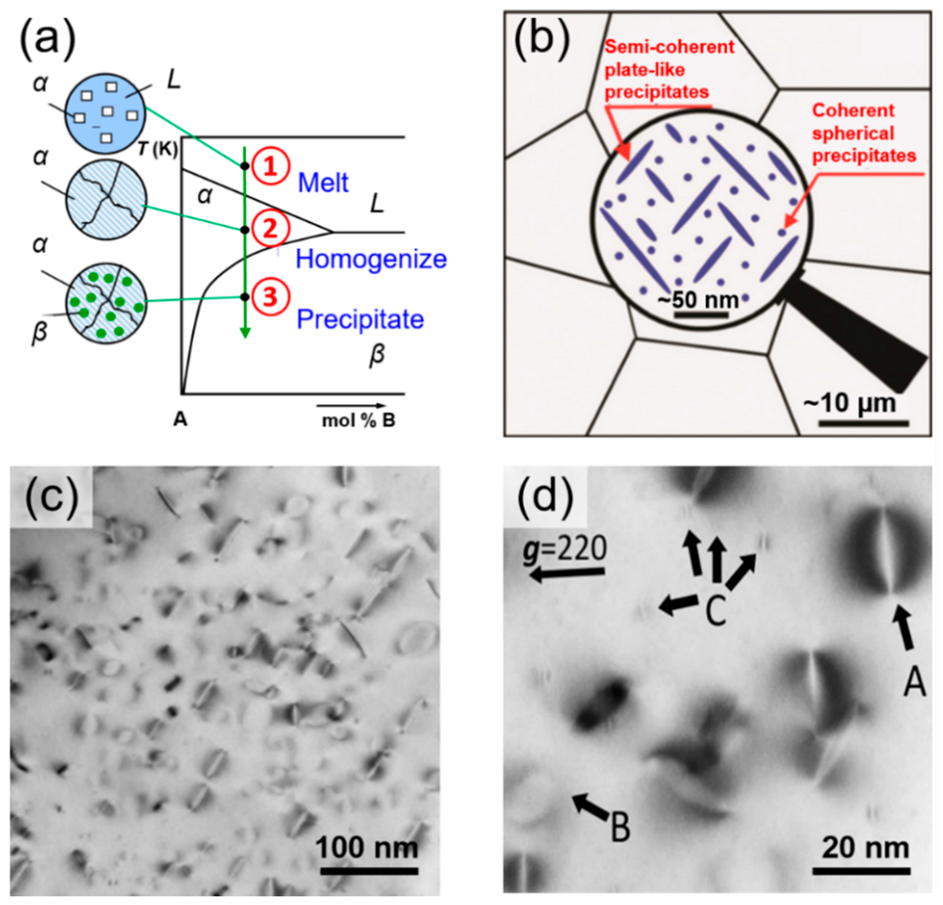
In the Si–P phase diagram [37], the solubility of P in Si is largely temperature-dependent. At high temperature, a small percentage of P can dissolve into Si; at room temperature, almost no P dissolves. Therefore, when a melt of highly P-doped Si cools from the α-phase region (Figure 1a), it is expected that P-rich precipitates form in the Si matrix. By using this method, our group has successfully synthesized nanostructured bulk Si [26]. We confirmed that two types of precipitates form in the Si matrix: semi-coherent plate-shaped precipitates of several dozen nanometers and coherent spherical-shaped precipitates of a few nanometers in size, as shown in Figure 1b–d. Transmission electron microscopy/energy-dispersive X-ray spectroscopy (TEM/EDS) analysis reveals that the precipitates are Si–P binary compounds. The EDS point-analysis has revealed that the precipitates are a Si–P binary compound. However, because the size of the precipitates is too small for the quantitative EDS analysis, the chemical composition, that is, the Si/P ratio has not been determined.
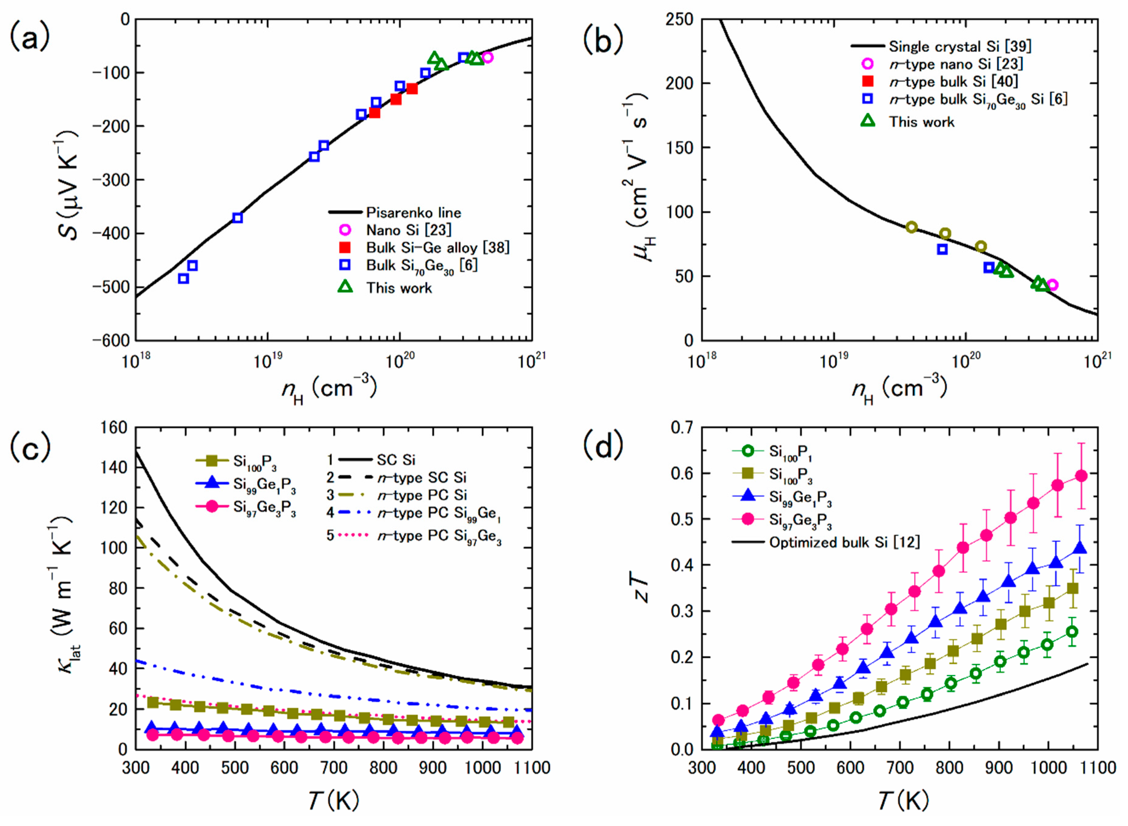
To understand the effects of the precipitates on the electrical properties, we added theoretically predicted lines on the S vs. nH relationship (Figure 2a) and the µH vs. nH relationship (Figure 2b), where nH and µH are the Hall carrier concentration and the Hall mobility, respectively. The line added on the S vs. nH relationship is called the Pisarenko line. Moreover, the literature values from References [38,39,40] were added for comparison. As shown in Figure 2a,b, all experimental S and μH values of nanostructured bulk Si are on the Pisarenko line and the line obtained by fitting the literature data for non-nanostructured Si, respectively, meaning that the nanoscale precipitates do not significantly affect the electrical properties. However, the κlat of nanostructured bulk Si are much lower than that of single crystalline (SC), heavily doped single crystalline Si (n-type SC Si), and heavily doped polycrystalline Si (n-type PC Si), as shown in Figure 2c. These low κlat values mainly arise from phonon scattering by the nanoscale precipitates. The maximum zT value approaches 0.6 at 1050 K for nanostructured bulk Si containing 3% Ge; this is approximately three times higher than the zT value of optimized bulk Si, as shown in Figure 2d.
3. Synthesis and Size Control of Si and Metal Silicide Nanocomposites by Melt-Spinning
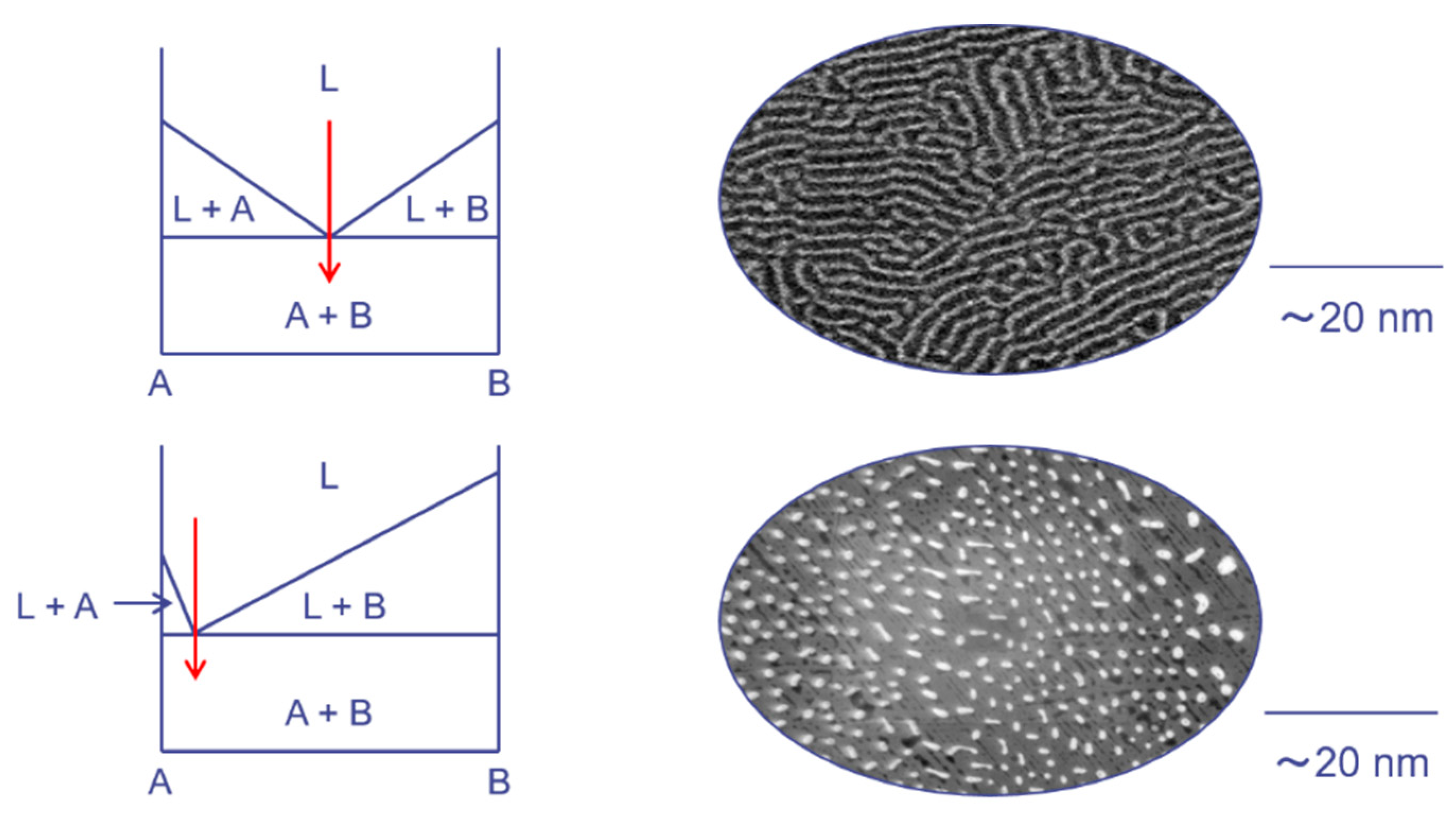
At the eutectic composition, nanocomposites with homogeneous distributions of secondary phases in the primary-phase matrix can be obtained. Several metal silicides may form such nanoscale precipitates in Si matrices because they have a pseudo-binary eutectic point with Si. As summarized in Figure 3, the structural characteristic of the secondary phase, i.e., nano-lamellar or nano-dot, depends on the position of the eutectic point. Among various metal silicides, CrSi2, CoSi2, and TiSi2 have eutectic points with Si at intermediate dopant concentrations, while VSi2 has a eutectic point with Si at low V concentrations.
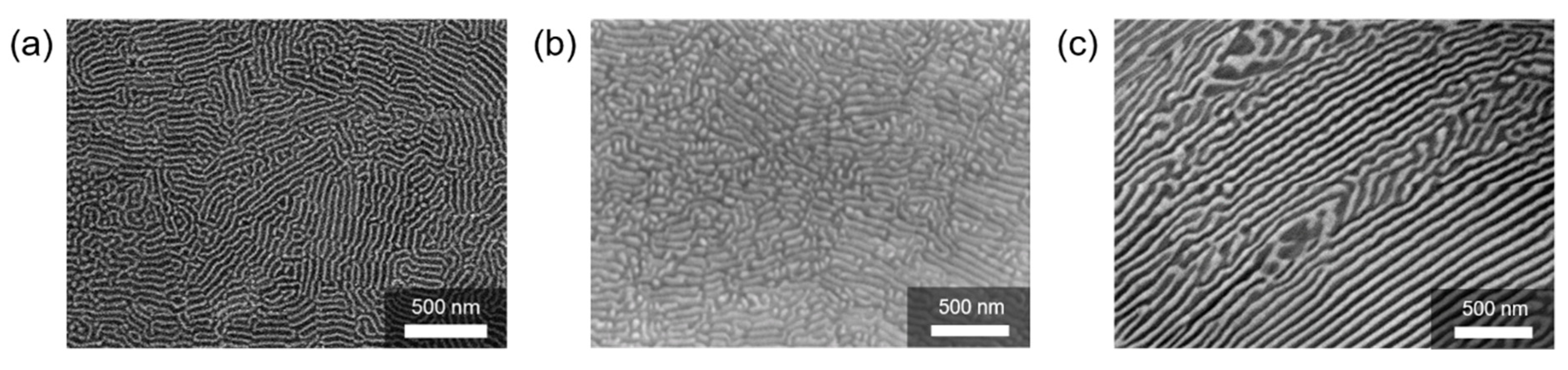
Figure 4 shows scanning electron microscopy (SEM) images of the nano-lamellar structures obtained by MS at the eutectic points between Si and various metal silicides. All composites comprised two phases, i.e., white and dark areas corresponding to the metal silicide and Si matrix, respectively. The TE properties of the Si–CrSi2 system (thin ribbons) and the Si–CoSi2 system (bulk samples) have been characterized and reported by the authors’ group in reference number [32] and [33], respectively.
As shown in Figure 5, the nano-dot structure was obtained in the Si–VSi2 system at the eutectic composition. Because the eutectic point existed at very low V contents (3 at.% V), the nano-dot structure was obtained. Moreover, the dot size was controlled by adjusting the cooling speed, that is, higher cooling rates corresponded to smaller dots, as summarized in Figure 5 and Figure 6. The VSi2 nano-precipitates scattered phonons more effectively than charge carriers, thus enhancing zT by approximately 40%; it was maximized at 0.23 at 1070 K [34].
4. Promising New Metal Silicide for TE Devices
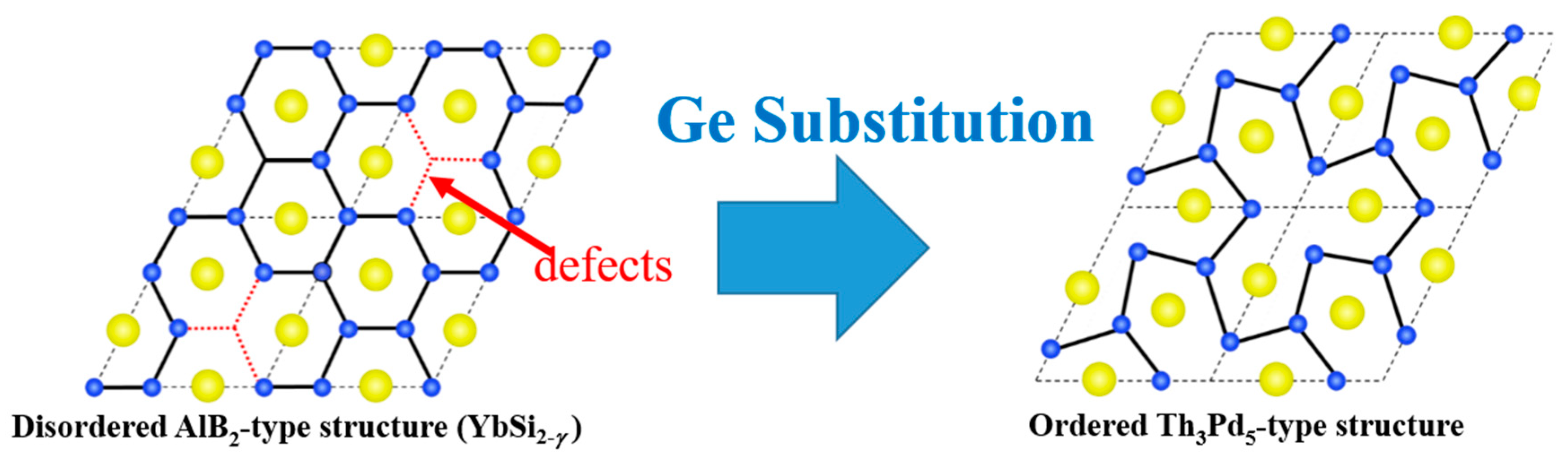
Our group has discovered that YbSi2−δ exhibits a high power factor of 2.2 mW·m−1·K−2 at room temperature [35]. Because of the mixed valence behavior of Yb, YbSi2−δ has an extraordinarily high S value despite its metallically high σ. Furthermore, we have demonstrated that the power factor of YbSi2−δ can be improved by substituting Si by Ge. The substitution gradually changed the structure from AlB2 type with random defects to Th3Pd5 type with ordered defects, reducing the level of disordered defects, as shown in Figure 7.
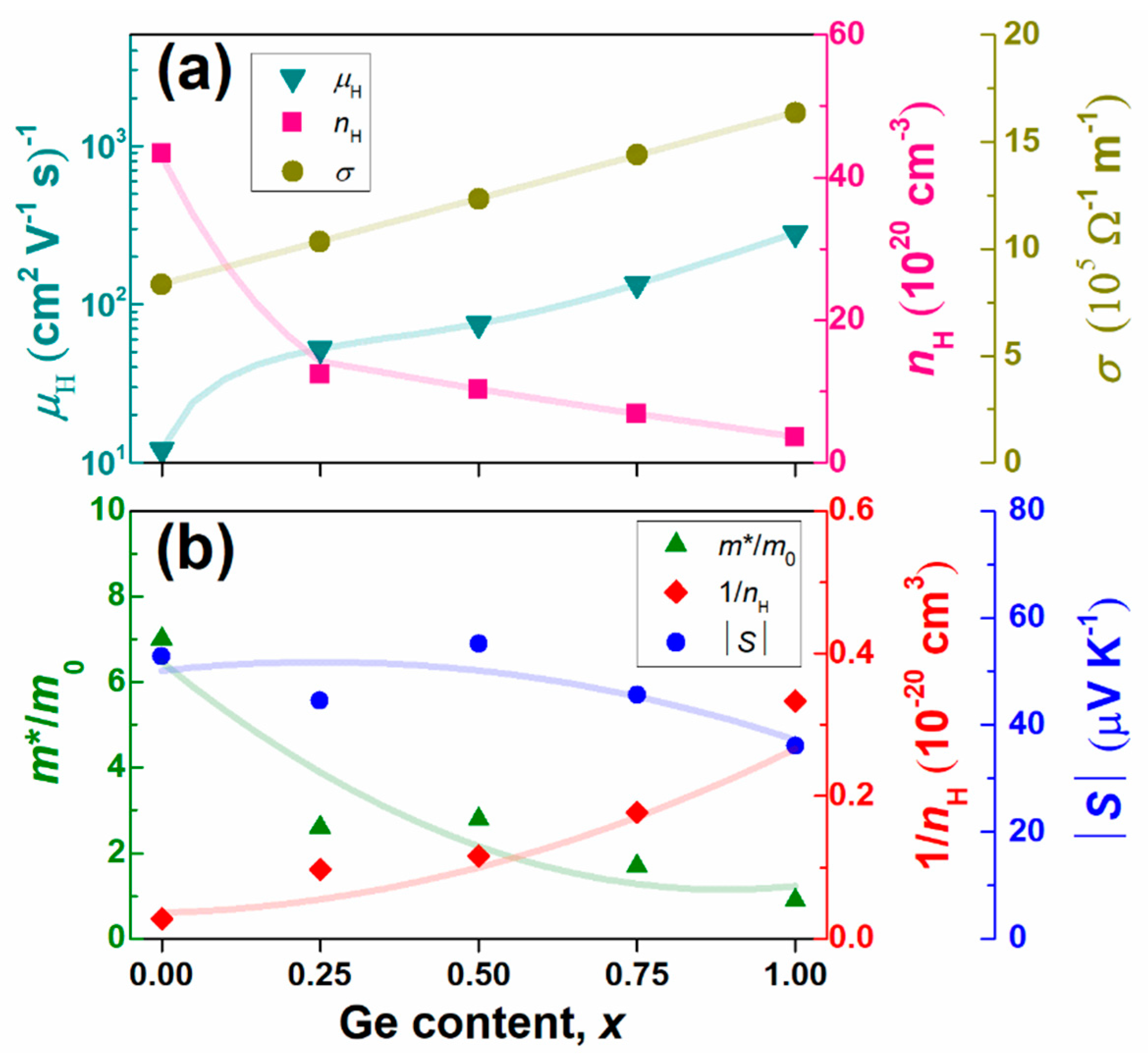
The composition dependences of the Hall mobility µH, Hall concentration nH, and σ (=e·µH·nH) values are shown in Figure 8a. The nH values decreased with the increasing Ge content, possibly because of the reduced density of states near the Fermi level. Moreover, the valence states of Yb in the compounds tended to decrease from 3+ to 2+ with the increasing Ge content, which may reduce the number of conduction-band electrons, thus reducing nH. Meanwhile, µH values increased considerably with the increasing Ge content, possibly because of changes in the band structure, reductions in electron scattering, and the removal of disordered defects in the Si sub-lattices via the structural transition discussed above. Based on the results of nH and µH, the electrical conductivity σ (=e·µH·nH) was increased approximately linearly with the Ge content.
Figure 9 shows the electrical properties of polycrystalline bulk samples of Yb(Si1−xGex)2−δ (x = 0.25, 0.50, 0.75, and 1.0). The negative values of S indicate that electrons were the majority charge carriers; the absolute S was maximized at x = 0.5. As shown in Figure 8b, the values of m*/m0 and 1/nH show trends opposing those with the Ge content, meaning that an optimized Ge content existed at which the absolute S was maximized. The values of σ increased with the increasing Ge content, mainly because of the increased μH. The maximum S2σ value was 3.6 mW·m−1·K−2 at room temperature at x = 0.5; this value is comparable to or higher than those of conventional TE materials such as Bi2Te3.
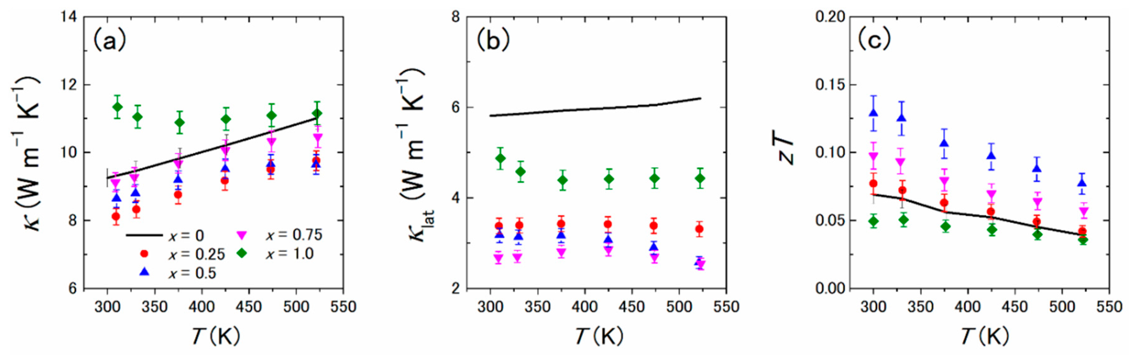
Figure 10a–c show the temperature dependences of κ, κlat, and zT of Yb(Si1−xGex)2−δ (x = 0–1.0). As can be seen in Figure 10b, the samples with x = 0.25, 0.50, and 0.75 had lower κlat values than those with x = 0 and 1, mainly due to the phonon scattering of Si/Ge substitution. The enhanced power factor and reduced κlat led to an improvement of zT for x = 0.25, 0.50, and 0.75, as can be seen in Figure 10c. The maximum zT value was 0.13 at room temperature obtained for the sample with x = 0.5.
5. Summary
In this review, recent research toward the development of high-efficiency eco-friendly Si-based TE materials was summarized. When a melt of highly P-doped Si is cooled from the α-phase, Si–P binary precipitates form naturally in the Si matrix, yielding nanostructured bulk Si. The nanoscale precipitates reduce κlat without significantly affecting the electron transport properties, thus enhancing zT. In addition to this natural nanostructuring procedure, our group has proposed the rapid-solidification MS method to synthesize Si–metal silicide nanocomposites. At the eutectic composition of Si and a given metal silicide, a eutectic structure with a homogeneous dispersion of metal silicides in the Si matrix can be obtained. Furthermore, with varied cooling rates, the eutectic structure feature size can be controlled, that is, higher cooling rates correspond to smaller sizes, as demonstrated in the Si–VSi2 system. Finally, we have discovered a promising high-power-factor TE metal silicide, YbSi2. Because of the mixed valence state of Yb, this metal silicide exhibits a large S with a metallically high σ, yielding a high room-temperature power factor. Furthermore, the power factor can be enhanced by the substitution of Ge for Si.
Author Contributions
Conceptualization, S.-a.T. and K.K.; Methodology, S.-a.T. and K.K.; Validation, S.-a.T. and K.K.; Formal Analysis, S.-a.T. and K.K.; Writing-Original Draft Preparation, S.-a.T. and K.K.; Writing-Review & Editing, S.-a.T. and K.K.; Visualization, S.-a.T. and K.K.; Supervision, K.K.
Funding
This research was funded by [JST, PRESTO] grant number [JPMJPR15R1].
Acknowledgments
The results of the YbSi2 part were obtained under the collaboration with Hitachi, Ltd.
Conflicts of Interest
The authors declare no conflicts of interest.
References
- Bell, L.E. Cooling, Heating, Generating Power, and Recovering Waste Heat with Thermoelectric Systems. Science 2008, 321, 1457–1461. [Google Scholar] [CrossRef] [PubMed] [Green Version]
- Snyder, G.J.; Toberer, E.S. Complex Thermoelectric Materials. Nat. Mater. 2008, 7, 105–114. [Google Scholar] [CrossRef] [PubMed]
- Venkatasubramanian, R.; Siivola, E.; Colpitts, T.; O’Quinn, B. Thin-Film Thermoelectric Devices with High Room-Temperature Figures of Merit. Nature 2001, 413, 597–602. [Google Scholar] [CrossRef] [PubMed]
- Heremans, J.P.; Jovovic, V.; Toberer, E.S.; Saramat, A.; Kurosaki, K.; Charoenphakdee, A.; Yamanaka, S.; Snyder, G.J. Enhancement of Thermoelectric Efficiency in PbTe by Distortion of the Electronic Density of States. Science 2008, 321, 554–557. [Google Scholar] [CrossRef] [PubMed] [Green Version]
- Steele, M.C.; Rosi, F.D. Thermal Conductivity and Thermoelectric Power of Germanium Silicon Alloys. J. App. Phys. 1958, 29, 1517–1520. [Google Scholar] [CrossRef]
- Dismukes, J.P.; Ekstrom, L.; Steigmeier, E.F.; Kudman, I.; Beers, D.S. Thermal and Electrical Properties of Heavily Doped Ge-Si Alloys up to 1300 K. J. Appl. Phys. 1964, 35, 2899–2907. [Google Scholar] [CrossRef]
- Zaitsev, V.K.; Fedorov, M.I.; Gurieva, E.A.; Eremin, I.S.; Konstantinov, P.P.; Samunin, A.Y.; Vedernikov, M.V. Highly Effective Mg2Si1−xSnx Thermoelectrics. Phys. Rev. B 2006, 74, 045207. [Google Scholar] [CrossRef]
- Liu, W.; Tan, X.; Yin, K.; Liu, H.; Tang, X.; Shi, J.; Zhang, Q.; Uher, C. Convergence of Conduction Bands as a Means of Enhancing Thermoelectric Performance of n-Type Mg2Si1-xSnx Solid Solutions. Phys. Rev. Lett. 2012, 108, 166601. [Google Scholar] [CrossRef] [PubMed]
- Zaitsev, V.K. Thermoelectrics Handbook; Rowe, D.M., Ed.; CRC Press: Boca Raton, FL, USA, 1995. [Google Scholar]
- Fedorov, M.I.; Zaitsev, V.K. Thermoelectrics Handbook; Rowe, D.M., Ed.; CRC Press: Boca Raton, FL, USA, 2006; p. 3. [Google Scholar]
- Weber, L.; Gmelin, E. Transport Properties of Silicon. Appl. Phys. A 1991, 53, 136–140. [Google Scholar] [CrossRef]
- Zhu, G.H.; Lee, H.; Lan, Y.; Wang, X.; Joshi, G.; Wang, D.; Yang, J.; Vashaee, D.; Guilbert, H.; Pillitteri, A.; et al. Increased Phonon Scattering by Nanograins and Point Defects in Nanostructured Silicon with a Low Concentration of Germanium. Phys. Rev. Lett. 2009, 102, 196803. [Google Scholar] [CrossRef] [PubMed]
- Tritt, T.M. Holey and Unholey Semiconductors. Science 1999, 283, 804–805. [Google Scholar] [CrossRef]
- Xie, H.H.; Wang, H.; Pei, Y.Z.; Fu, C.G.; Liu, X.H.; Snyder, G.J.; Zhao, X.B.; Zhu, T.J. Beneficial Contribution of Alloy Disorder to Electron and Phonon Transport in Half-Heusler Thermoelectric Materials. Adv. Funct. Mater. 2013, 23, 5123–5130. [Google Scholar] [CrossRef]
- Sales, B.C.; Mandrus, D.; Williams, R.K. Filled Skutterudite Antimonides: A New Class of Thermoelectric Materials. Science 1996, 272, 1325–1328. [Google Scholar] [CrossRef] [PubMed]
- Shi, X.; Yang, J.; Salvador, J.R.; Chi, M.; Cho, J.Y.; Wang, H.; Bai, S.; Yang, J.; Zhang, W.; Chen, L. Multiple-Filled Skutterudites: High Thermoelectric Figure of Merit through Separately Optimizing Electrical and Thermal Transports. J. Am. Chem. Soc. 2011, 133, 7837–7846. [Google Scholar] [CrossRef]
- Nielsen, M.D.; Ozolins, V.; Heremans, J.P. Lone Pair Electrons Minimize Lattice Thermal Conductivity. Energy Environ. Sci. 2013, 6, 570–578. [Google Scholar] [CrossRef]
- Zhao, L.D.; Lo, S.H.; Zhang, Y.; Sun, H.; Tan, G.; Uher, C.; Wolverton, C.; Dravid, V.P.; Kanatzidis, M.G. Ultralow Thermal Conductivity and High Thermoelectric Figure of Merit in SnSe Crystals. Nature 2014, 508, 373–377. [Google Scholar] [CrossRef] [PubMed]
- Poudel, B.; Hao, Q.; Ma, Y.; Lan, Y.; Minnich, A.; Yu, B.; Yan, X.; Wang, D.; Muto, A.; Vashaee, D.; et al. High-Thermoelectric Performance of Nanostructured Bismuth Antimony Telluride Bulk Alloys. Science 2008, 320, 634–638. [Google Scholar] [CrossRef] [Green Version]
- Biswas, K.; He, J.; Blum, I.D.; Wu, C.I.; Hogan, T.P.; Seidman, D.N.; Dravid, V.P.; Kanatzidis, M.G. High-Performance Bulk Thermoelectrics with All-Scale Hierarchical Architectures. Nature 2012, 489, 414–418. [Google Scholar] [CrossRef] [PubMed]
- Hochbaum, A.I.; Chen, R.; Delgado, R.D.; Liang, W.; Garnett, E.C.; Najarian, M.; Majumdar, A.; Yang, P. Enhanced Thermoelectric Performance of Rough Silicon Nanowires. Nature 2008, 451, 163–167. [Google Scholar] [CrossRef] [PubMed]
- Boukai, A.I.; Bunimovich, Y.; Tahir-Kheli, J.; Yu, J.K.; Goddard, W.A.; Heath, J.R. Silicon Nanowires as Efficient Thermoelectric Materials. Nature 2008, 451, 168–171. [Google Scholar] [CrossRef]
- Bux, S.K.; Blair, R.G.; Gogna, P.K.; Lee, H.; Chen, G.; Dresselhaus, M.S.; Kaner, R.B.; Fleurial, J.P. Nanostructured Bulk Silicon as an Effective Thermoelectric Material. Adv. Funct. Mater. 2009, 19, 2445–2452. [Google Scholar] [CrossRef]
- Dresselhaus, M.S.; Chen, G.; Tang, M.Y.; Yang, R.; Lee, H.; Wang, D.; Ren, Z.; Fleurial, J.P.; Gogna, P. New Directions for Low-Dimensional Thermoelectric Materials. Adv. Mater. 2007, 19, 1043–1053. [Google Scholar] [CrossRef]
- Kurosaki, K.; Yusufu, A.; Miyazaki, Y.; Ohishi, Y.; Muta, H.; Yamanaka, S. Enhanced Thermoelectric Properties of Silicon via Nanostructuring. Mater. Trans. 2016, 57, 1018–1021. [Google Scholar] [CrossRef]
- Yusufu, A.; Kurosaki, K.; Miyazaki, Y.; Ishimaru, M.; Kosuga, A.; Ohishi, Y.; Muta, H.; Yamanaka, S. Bottom-Up Nanostructured Bulk Silicon: A Practical High-Efficiency Thermoelectric Material. Nanoscale 2014, 6, 13921–13927. [Google Scholar] [CrossRef] [PubMed]
- Xie, W.; He, J.; Kang, H.J.; Tang, X.; Zhu, S.; Laver, M.; Wang, S.; Copley, J.R.D.; Brown, C.M.; Zhang, Q.; et al. Identifying the Specific Nanostructures Responsible for the High Thermoelectric Performance of (Bi,Sb)2Te3 Nanocomposites. Nano Lett. 2010, 10, 3283–3289. [Google Scholar] [CrossRef]
- Tang, X.; Xie, W.; Li, H.; Zhao, W.; Zhang, Q.; Niino, M. Preparation and Thermoelectric Transport Properties of High-Performance p-type Bi2Te3 with Layered Nanostructure. Appl. Phys. Lett. 2007, 90, 012102. [Google Scholar] [CrossRef]
- Li, H.; Tang, X.; Su, X.; Zhang, Q. Preparation and Thermoelectric Properties of High-Performance Sb Additional Yb0.2Co4Sb12+y Bulk Materials with Nanostructure. Appl. Phys. Lett. 2008, 92, 202114. [Google Scholar] [CrossRef]
- Li, H.; Tang, X.; Zhang, Q.; Uher, C. Rapid Preparation Method of Bulk Nanostructured Yb0.3Co4Sb12+y Compounds and Their Improved Thermoelectric Performance. Appl. Phys. Lett. 2008, 93, 252109. [Google Scholar] [CrossRef]
- Tan, L.P.; Sun, T.; Fan, S.; Ramanujan, R.V.; Hng, H.H. Facile Precipitation of Two Phase Alloys in SnTe0.75Se0.25 with Improved Power Factor. J. Alloys Compd. 2014, 587, 420–427. [Google Scholar] [CrossRef]
- Norizan, M.N.; Miyazaki, Y.; Ohishi, Y.; Muta, H.; Kurosaki, K.; Yamanaka, S. The Nanometer-Sized Eutectic Structure of Si/CrSi2 Thermoelectric Materials Fabricated by Rapid Solidification. J. Electron. Mater. 2018, 47, 2330–2336. [Google Scholar] [CrossRef]
- Xie, J.; Ohishi, Y.; Ichikawa, S.; Muta, H.; Kurosaki, K.; Yamanaka, S. Thermoelectric Properties of Si/CoSi2 Sub-Micrometer Composites Prepared by Melt-Spinning Technique. J. Appl. Phys. 2017, 121, 205107. [Google Scholar] [CrossRef]
- Tanusilp, S.; Kurosaki, K.; Yusufu, A.; Ohishi, Y.; Muta, H.; Yamanaka, S. Enhancement of Thermoelectric Properties of Bulk Si by Dispersing Size-Controlled VSi2. J. Electron. Mater. 2017, 46, 3249–3255. [Google Scholar] [CrossRef]
- Tanusilp, S.; Ohishi, Y.; Muta, H.; Yamanaka, S.; Nishide, A.; Hayakawa, J.; Kurosaki, K. Ytterbium Silicide (YbSi2): A Promising Thermoelectric Material with a High Power Factor at Room Temperature. Phys. Status Solidi RRL 2018, 12, 1700372. [Google Scholar] [CrossRef]
- Tanusilp, S.; Ohishi, Y.; Muta, H.; Nishide, A.; Hayakawa, J.; Kurosaki, K. High Thermoelectric Power Factor of Ytterbium Silicon-Germanium. Appl. Phys. Lett. 2018, 113, 193901. [Google Scholar] [CrossRef]
- Olesinski, R.W.; Kanani, N.; Abbaschian, G.J. The P-Si (Phosphorus-Silicon) System. Bull. Alloy Phase Diagr. 1985, 6, 128–130. [Google Scholar] [CrossRef]
- Golikova, O.A.; Iordanishvili, E.K.; Petrov, A.V.; Tela, F.T. Electrical properties of solid solutions in the Si-Ge system (Electric conductivity and thermal emf of solid solutions of silicon-germanium with near silicon composition and various current-carrier concentrations and test temperatures). Sov. Phys. Solid State 1966, 8, 397–401. [Google Scholar]
- Masetti, G.; Severi, M.; Solmi, S. Modeling of Carrier Mobility against Carrier Concentration in Arsenic-, Phosphorus-, and Boron-Doped Silicon. IEEE Trans. Electron Devices 1983, 30, 764–769. [Google Scholar] [CrossRef]
- Morin, F.; Maita, J. Electrical Properties of Silicon Containing Arsenic and Boron. Phys. Rev. 1954, 96, 28–35. [Google Scholar] [CrossRef]
Figure 1.
(a) Precipitates naturally form when the melt cools from the α-phase region in a binary phase diagram. (b) Micro- and nanoscale schematics of a nanostructured bulk material containing various types of precipitates. (c) Low- and (d) high-magnification bright-field transmission electron microscopy (TEM) images of nanostructured bulk Si, showing the homogeneous distribution of nanoscale precipitates in the Si matrix. Contrast shows strain arising from the precipitates. In (d), the arrows A and B indicate plate-like precipitates along (high contrast) and perpendicular (lesser contrast) to the electron beam, respectively. The arrow C indicates very small (the average diameter < 5 nm) precipitates with a butterfly-like shade. Reproduced with permission from Ref. [26]. Copyright 2009, the Royal Society of Chemistry.

Figure 2.
(a) Seebeck coefficient S and (b) Hall carrier mobility μH as a function of Hall carrier concentration nH at 300 K for various types of Si. Temperature dependences of (c) lattice thermal conductivity κlat and (d) dimensionless figure of merit zT of nanostructured bulk Si containing small amounts of Ge. Reproduced with permission from Ref. [26]. Copyright 2009, the Royal Society of Chemistry.

Figure 3.
Relationship between phase diagram and nanostructure. According to the position of the eutectic point, nano-lamellar or nano-dot structure can be obtained by melt-spinning (MS).
Figure 3.
Relationship between phase diagram and nanostructure. According to the position of the eutectic point, nano-lamellar or nano-dot structure can be obtained by melt-spinning (MS).

Figure 4.
Scanning electron microscopy (SEM) images of nano-lamellar structures obtained by MS at the eutectic points between Si and metal silicides: (a) Si–CrSi2, (b) Si–CoSi2, and (c) Si–TiSi2.
Figure 4.
Scanning electron microscopy (SEM) images of nano-lamellar structures obtained by MS at the eutectic points between Si and metal silicides: (a) Si–CrSi2, (b) Si–CoSi2, and (c) Si–TiSi2.

Figure 5.
SEM images of nano-dot structures obtained by MS at the eutectic point between Si and VSi2, showing that larger cooling rates yield smaller dot sizes. Reproduced with permission from Ref. [34]. Copyright 2016, Springer Nature.
Figure 5.
SEM images of nano-dot structures obtained by MS at the eutectic point between Si and VSi2, showing that larger cooling rates yield smaller dot sizes. Reproduced with permission from Ref. [34]. Copyright 2016, Springer Nature.
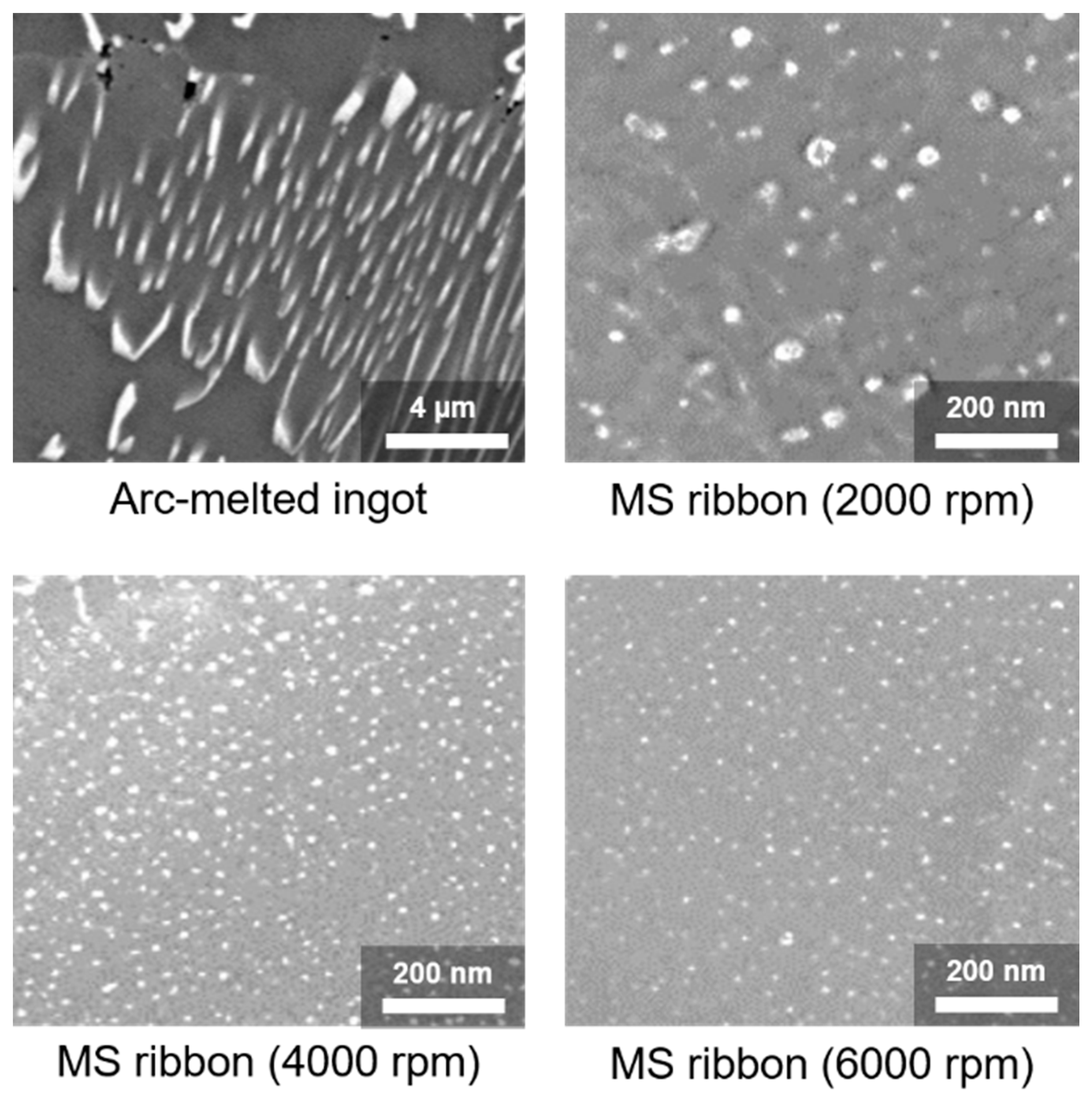
Figure 6.
Schematics comparing micro- and nanocomposites synthesized by (a) arc melting (normal cooling rate) and (b) MS (high cooling rate). Reproduced with permission from Ref. [34]. Copyright 2016, Springer Nature.
Figure 6.
Schematics comparing micro- and nanocomposites synthesized by (a) arc melting (normal cooling rate) and (b) MS (high cooling rate). Reproduced with permission from Ref. [34]. Copyright 2016, Springer Nature.
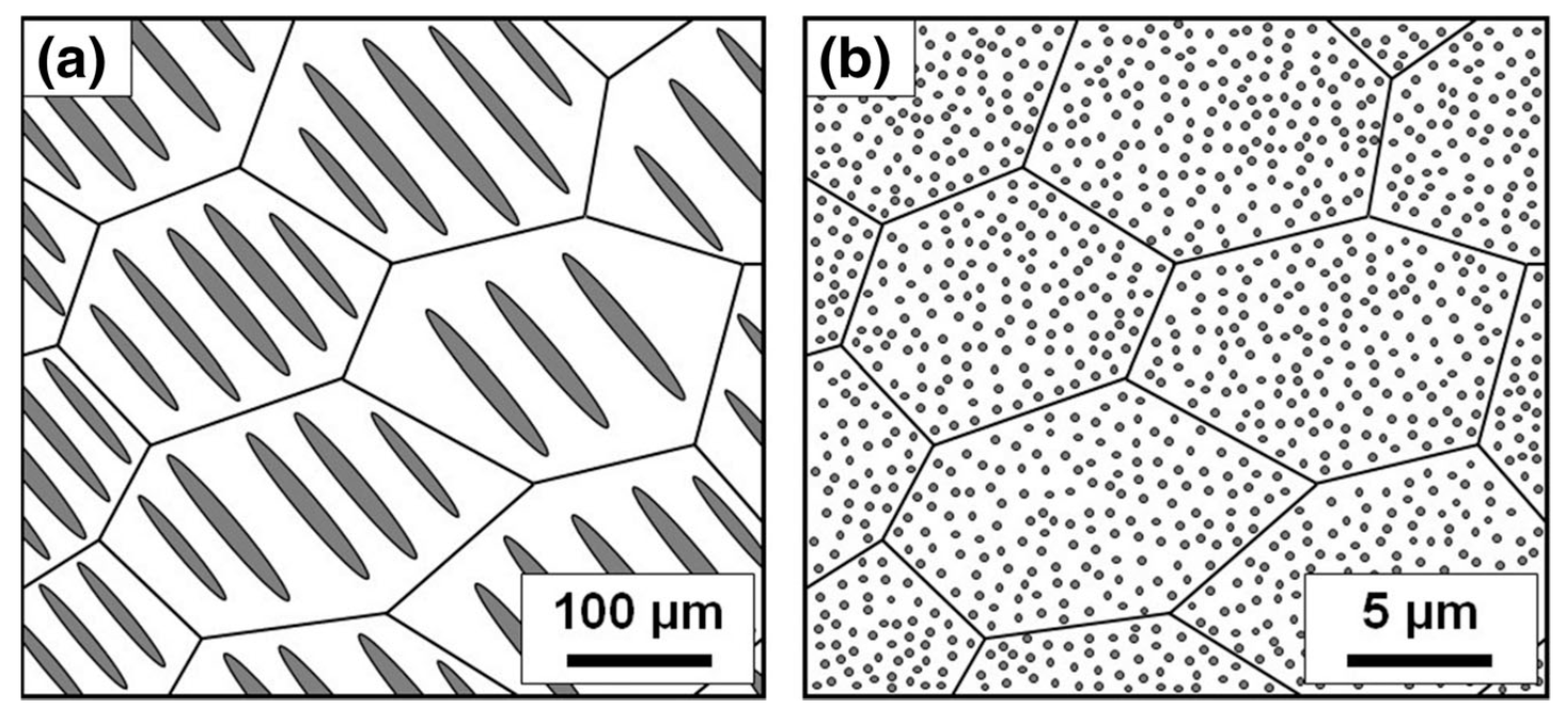
Figure 7.
Schematic of crystal structure of YbSiGe projected along the c axis, showing a structural transition from the disordered AlB2-type structure to the ordered Th3Pd5-type structure. Yellow and blue balls represent Yb and Si/Ge, respectively. Reproduced with permission from Ref. [36]. Copyright 2018, AIP Publishing.

Figure 8.
Composition dependences of (a) the Hall mobility µH, Hall concentration nH, and electrical conductivity σ (=e·µH·nH) and (b) absolute S |S|, effective mass m*/m0, and 1/nH for Yb(Si1−xGex)2−δ (0 ≤ x ≤ 1.0). All symbols represent experimental data obtained at 300 K. The lines are guides to the eye. Reproduced with permission from Ref. [36]. Copyright 2018, AIP Publishing.

Figure 9.
Temperature dependences of (a) the Seebeck coefficient S, (b) electrical conductivity σ, and (c) power factor S2σ of polycrystalline bulk samples of Yb(Si1−xGex)2−δ (x = 0, 0.25, 0.50, 0.75, and 1.0). Reproduced with permission from Ref. [36]. Copyright 2018, AIP Publishing.
Figure 9.
Temperature dependences of (a) the Seebeck coefficient S, (b) electrical conductivity σ, and (c) power factor S2σ of polycrystalline bulk samples of Yb(Si1−xGex)2−δ (x = 0, 0.25, 0.50, 0.75, and 1.0). Reproduced with permission from Ref. [36]. Copyright 2018, AIP Publishing.
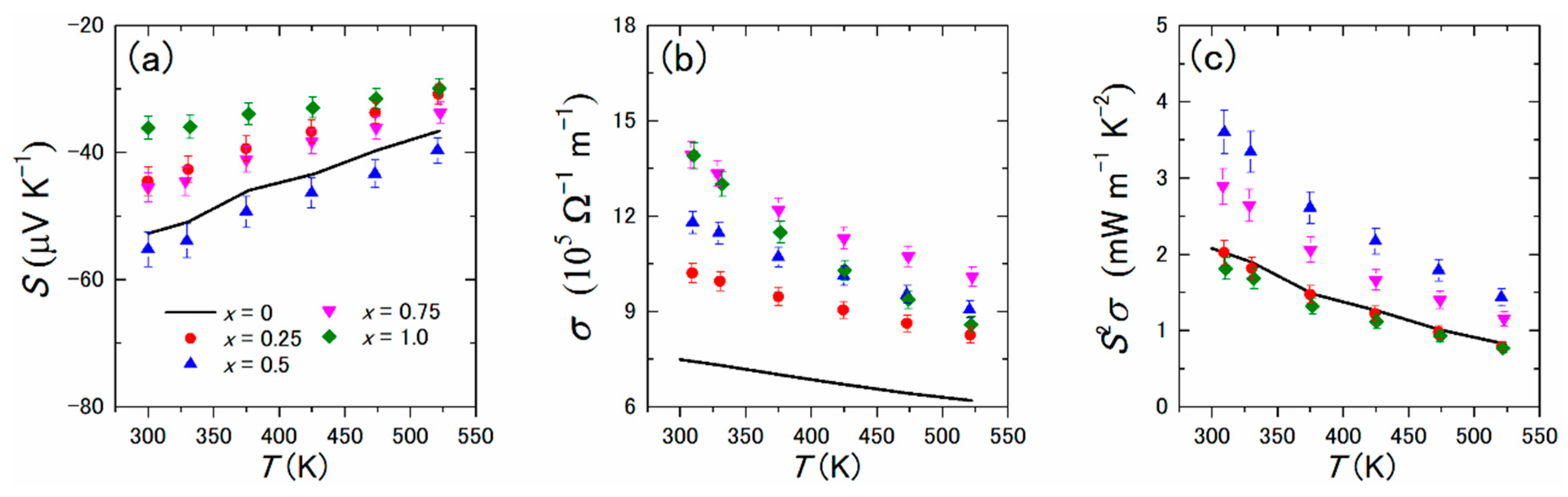
Figure 10.
Temperature dependences of (a) total thermal conductivity κ, (b) lattice thermal conductivity κlat, and (c) dimensionless figure of merit zT for polycrystalline bulk samples of Yb(Si1−xGex)2−δ (x = 0, 0.25, 0.50, 0.75, and 1.0). Reproduced with permission from Ref. [36]. Copyright 2018, AIP Publishing.

© 2019 by the authors. Licensee MDPI, Basel, Switzerland. This article is an open access article distributed under the terms and conditions of the Creative Commons Attribution (CC BY) license (http://creativecommons.org/licenses/by/4.0/).
Share and Cite
MDPI and ACS Style
Tanusilp, S.-a.; Kurosaki, K. Si-Based Materials for Thermoelectric Applications. Materials 2019, 12, 1943. https://doi.org/10.3390/ma12121943
AMA Style
Tanusilp S-a, Kurosaki K. Si-Based Materials for Thermoelectric Applications. Materials. 2019; 12(12):1943. https://doi.org/10.3390/ma12121943
Chicago/Turabian StyleTanusilp, Sora-at, and Ken Kurosaki. 2019. "Si-Based Materials for Thermoelectric Applications" Materials 12, no. 12: 1943. https://doi.org/10.3390/ma12121943
Note that from the first issue of 2016, this journal uses article numbers instead of page numbers. See further details here.