Improvements on the Interfacial Properties of High-k/Ge MIS Structures by Inserting a La2O3 Passivation Layer


Key Laboratory for Wide Band Gap Semiconductor Materials and Devices of Education, School of Microelectronics, Xidian University, Xi’an 710071, China
*
Authors to whom correspondence should be addressed.
Materials 2018, 11(11), 2333; https://doi.org/10.3390/ma11112333
Submission received: 30 October 2018
/
Revised: 15 November 2018
/
Accepted: 17 November 2018
/
Published: 20 November 2018
(This article belongs to the Section Advanced Materials Characterization)
Abstract
:In this paper, the impact of La2O3 passivation layers on the interfacial properties of Ge-based metal-insulator-semiconductor (MIS) structures was investigated. It was proven that the formation of a thermodynamically stable LaGeOx component by incorporating a La2O3 interlayer could effectively suppress desorption of the interfacial layer from GeO2 to volatile GeO. The suppression of GeO desorption contributed to the decrease in oxide trapped charges and interfacial traps in the bulk of the gate insulator, or the nearby interfacial regions in the Al2O3/La2O3/Ge structure. Consequently, the hysteretic behavior of the dual-swept capacitance-voltage (C-V) curves and the frequency dispersion of multi-frequency C-V curves were remarkably weakened. Besides, more than one order of magnitude decrease in the gate leakage current density, and higher insulator breakdown electric field were obtained after inserting a La2O3 passivation layer.
1. Introduction
For a very long time, the excellent properties of a SiO2/Si interface, with high band offsets and few interfacial defects, have been the key reasons for supporting Si use as the main semiconductor material in integrated circuits (IC) [1]. However, with the continued scaling of the device’s size feature on a Si-based complementary metal oxide semiconductor (CMOS) process, high dielectric constant (high-k) materials have been introduced as alternative gate oxide dielectrics to replace ultrathin SiO2. The purpose was to reduce gate leakage current and power consumption beyond 45-nm technology nodes [2,3]. The introduction of high-k dielectrics into the Si-based CMOS process results in poorer insulator/Si interfaces compared to that of SiO2/Si, bringing in some unfavorable impacts such as instability problems and mobility degradation [4]. Considering this, alternative technological progress to dimension scaling, such as changing channel material, is also necessary for achieving high performance devices [5]. Owing to its high intrinsic hole mobility, Ge has drawn remarkable attention for realizing high performance applications in the past decade [6,7]. Ge-based metal-insulator-semiconductor (MIS) devices have shown great potential for integration into the Si CMOS technology, since promising electrical characteristics beyond those of Si devices could be realized by high-k/Ge structures [8]. However, there are some obstacles to overcome before employing Ge into a CMOS-compatible processing scheme with high performance. One of the most critical issues to solve is the Ge surface passivation engineering prior to the deposition of gate oxides [9]. For most high-k dielectric films deposited on Ge substrates without any surface passivation treatments, the generation of unstable Ge oxides is unavoidable during the thermal annealing process. That is, at temperatures higher than 400 °C, GeO2 reacts with Ge atoms at high-k dielectrics/Ge interface, which then form substoichiometric Ge oxides, including volatile GeO [10,11]. The desorption of GeO brings in a large number of structural defects, which would deteriorate the properties of the insulator/Ge interface [12].
Recently, it has been reported that rare earth oxides (REOs; i.e., Y2O3, CeO2, Sm2O3, and La2O3) show high affinity for Ge atoms. That is, the strong reaction between REOs and Ge substrates leads to the catalytic oxidation of Ge, which results in the spontaneous formation of stable interfacial layers [13,14,15,16]. Amongst the REOs, due to their large dielectric constant and high band offset relative to Ge, La-based oxides are considered as one kind of promising alternative gate dielectrics in Ge-based MIS devices, which can achieve more aggressive equivalent oxide thickness (EOT) scaling [17,18]. Furthermore, as the interface between La-based oxides and Ge substrates shows much better thermodynamic stability than that of GeO2/Ge, La-based oxides have promising interfacial passivation effects and could improve the electrical performance of Ge-based MIS devices [19,20]. Considering this, the effects of inserting a La2O3 passivation layer between an Al2O3 dielectric and Ge substrate, on the interfacial properties of Al/Al2O3/Ge and Al/Al2O3/La2O3/Ge MIS structures was investigated in this paper.
2. Experimental Section
La2O3 and Al2O3 gate stack films were deposited on n-type Ge (100) substrates, with electrical resistivity of about 0.1–1 Ω·cm, in an atomic layer deposition (ALD) reactor (R-150, Picosun, Espoo, Finland). Prior to the deposition, Ge substrates were treated with acetone and hydrous alcohol, and then cyclically dipped into a diluted HF solution (HF:H2O = 1:50) 5 times to remove the native GeOx layer. During the deposition process, La(i−PrCp)3 and trimethylaluminum (TMA) were used as La and Al precursors, respectively, while H2O was used as an oxidant. The precursors were alternately introduced to the reactor chamber, and were carried by high purity N2 (>99.999%). A typical ALD growth cycle for La2O3 was 0.3 s La(i−PrCp)3 pulse, followed by 4 s N2 purge and 0.3 s H2O pulse, followed by 9 s N2 purge. The Al2O3 ALD cycle structure was set as 0.1 s TMA pulse/3 s N2 purge/0.1 s H2O pulse/4 s N2 purge. By varying the number of ALD cycles, a 2 nm La2O3 oxide layer was deposited on the cleaned Ge substrate at 300 °C, followed by deposition of a 4 nm Al2O3 layer. For comparison, a control sample with only 6 nm Al2O3 as gate dielectrics was also prepared. After the deposition, rapid thermal annealing (RTA) was performed at 600 °C for 90 s in N2 ambient for both Al2O3/La2O3/Ge and Al2O3/Ge structures.
The surface morphology of the deposited films was monitored using atomic force microscopy (AFM, Dimension 3100, Veeco Digital Instruments by Bruker, Billerica, MA, USA) in tapping mode. The physical thickness was optically measured using Woollam M2000D spectroscopic ellipsometry (SE, Woollam Co. Inc., Lincoln, NE, USA) fitted with a Cauchy model. The chemical bonding state of the samples related to Ge substrates was examined by X-ray photoelectron spectroscopy (XPS, Axis Ultra DLD, Kratos Analytical, Manchester, UK) measurements. MIS capacitor structures were used to evaluate the electrical properties of the deposited films. Al was evaporated using electron-beam evaporation as a metal gate through a shadow mask with a diameter of 300 μm followed by a post metallization annealing (PMA) carried out in 97% N2/3% H2 ambient at 400 °C for 20 min to form a good Ohmic contact with gate dielectrics. Then the electrical properties of the fabricated MIS capacitors were evaluated using an Agilent B1500A parameter analyzer (Santa Clara, CA, USA).
3. Results and Discussion
The Ge 3d spectra of the samples with and without the La2O3 passivation layer are shown in Figure 1. During the analysis of XPS data, the C 1s peak extracted from adventitious carbon at 284.6 eV was chosen as a bonding energy calibration reference. Compared with Figure 1a, a noteworthy change in Figure 1b was the appearance of a LaGeOx peak, indicating that a LaGeOx component was generated after inserting a thin La2O3 interlayer. Besides, the Ge oxide (GeOx) spectra could be divided into four Gaussian–Lorentzian line shape peaks (Ge1+, Ge2+, Ge3+, and Ge4+), which were located at a higher binding energy with respect to the Ge0 peak, with energy shifts of 0.8, 1.8, 2.6, and 3.4 eV, respectively [21]. The existence of these GeOx species was caused by the formation of an interfacial layer between gate dielectric films and Ge substrates [22]. Among the Ge sub-oxides, GeO (Ge2+) is known to adversely affect interfacial properties in contrast to other Ge oxides (Ge1+ and Ge3+), since GeO volatilization would cause a huge number of structural defects [13]. Compared with the control sample, a visible reduction in the intensity of the Ge2+ peak was observed in the Al2O3/La2O3/Ge case, indicating that to a certain extent, the formation of GeO was restrained by inserting a La2O3 passivation layer. Besides, it was observed that the intensity of the Ge4+ peak increased a bit after inserting a La2O3 passivation layer. Such variations in Ge2+ and Ge4+ peaks displayed a reasonable self-consistency, which was mainly ascribed to the reduction of desorption from GeO2 (Ge4+) to GeO, benefiting from the generation of a thermodynamically stable LaGeOx component near the La2O3/Ge interface [23].
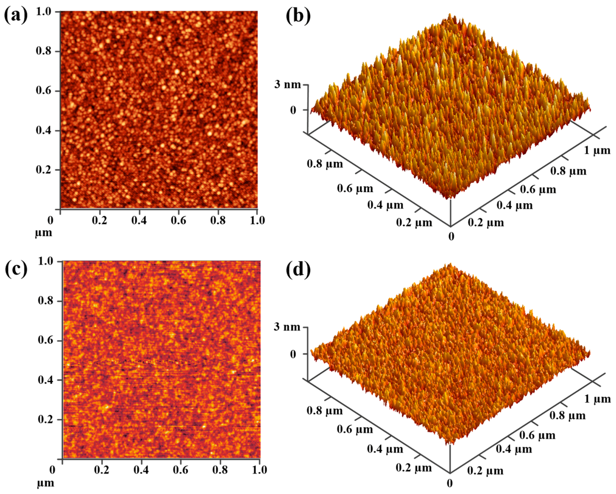
The two- and three-dimensional AFM images of the Al2O3 films deposited on Ge substrates with and without a La2O3 interlayer are shown in Figure 2. The scan size of each AFM image was 1 × 1 µm2. The root-mean-square (RMS) surface roughness of the films was extracted from the AFM images. The surface roughness of the sample without a La2O3 interlayer was about 0.62 nm in RMS, which was relatively a large RMS value for dielectric films deposited by ALD. We ascribed this large RMS value to the degradation of interfacial smoothness caused by the desorption of volatile GeO nearby the Al2O3/Ge interface during the high temperature post-deposition annealing (PDA) process [24]. While for the sample with a La2O3 interfacial passivation layer, an obviously smaller RMS value of 0.23 nm was observed. Such a reduction in the RMS value suggested that the desorption of GeO was suppressed since the existence of a thermodynamically stable LaGeOx layer between gate oxides and Ge substrates restrained the generation of volatile GeO. The decrease in volatile GeO had a positive impact on the electrical performance in the Al2O3/La2O3/Ge case. This improvement will be discussed in detail in the following capacitance-voltage (C-V) and gate leakage current density-voltage (J-V) parts.
To further investigate the effects of a La2O3 interfacial passivation layer on the interfacial properties of Ge-based MIS structures, the electrical properties of the fabricated MIS capacitors were analyzed. Figure 3 shows the C-V and conductance-voltage (G-V) characteristics of the fabricated MIS capacitors using Al2O3 as an insulator, with and without a La2O3 passivation layer. For simplicity, the MIS capacitor using only Al2O3 as an insulator was marked as S1, and the MIS capacitor with La2O3 as an interfacial passivation layer was assigned as S2. The dual-swept C-V curves were obtained by biasing the gate-applied voltage from accumulation to inversion (backward sweep), and sweeping back (forward sweep) at 100 kHz. G-V measurements were performed simultaneously with the backward swept C-V curves. The capacitance values at the accumulation region of the C-V curves for capacitor S1 and S2 were 1.06 and 1.41 μF/cm2, respectively. The dielectric constant values of the samples were estimated using the following equations [25,26]:
where Cac is the capacitance value at the accumulation region, Gac is the conductance corresponding to the accumulation region of the C-V curves, ω is the angular frequency, Cox is the oxide capacitance of dielectric films, A is the electrode area, tox is the measured thickness of gate dielectrics, and are the permittivity values of vacuum and SiO2, respectively. The physical thickness of the gate dielectric films in S1 and S2 was measured to be 6.42 and 6.83 nm, separately. Therefore, the effective dielectric constant values of S1 and S2 were calculated to be 7.95 and 11.10, respectively. The increment in the dielectric constant value for the sample with a La2O3 interfacial passivation layer was attributed to the introduction of La elements into dielectric films, since the k values of La2O3 [27], and LaxAlyO [28] formed by the interdiffusion of La2O3 and Al2O3 were much higher than that of Al2O3 [29].
The flat band voltages (VFB) of the C-V curves in Figure 3 were extracted from the Hauser NCSU CVC simulation software (North Carolina State University, Raleigh, NC, USA), taking quantum mechanical effects into account [30]. It was observed that the Al/Al2O3/Ge MIS capacitor showed a much larger flat band voltage hysteresis width (ΔVFB), ∼863 mV, than that of S2 (∼174 mV). The hysteretic behavior of the dual-swept C-V curves has been proven to be caused by the existence of oxide trapped charges (Qot) in the bulk of the gate insulator or nearby the interfacial region [31]. Using the midgap charge separation method, the oxide-trapped charge density (Not) for the fabricated capacitors was calculated using the following equation [32]:
where ΔVFB is the hysteresis width of VFB, Cox is the oxide capacitance, q is the elementary charge (1.602 × 10⁻¹⁹ C), and A is the electrode area. The Not values were calculated to be 5.91 × 1012 cm−2 for the Al/Al2O3/Ge MIS capacitor, and 1.56 × 1012 cm−2 for the case with a La2O3 passivation layer. A visible decrease of Not was observed after inserting a La2O3 passivation layer.
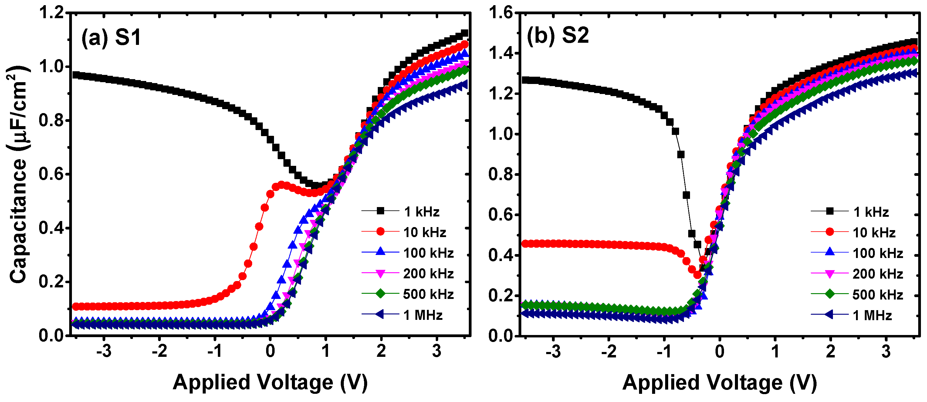
The C-V curves of the MIS capacitors without the La2O3 interlayer showed a significant anomalous hump phenomena at the weak inversion regions as shown in Figure 3a, which were reported to be caused by slow interfacial traps existing between the gate insulator and substrate [33]. Besides, as shown in Figure 4, different amounts of interfacial traps caused different degrees of frequency dispersion phenomena at the weak inversion regions of the C-V curves measured at multi-frequencies. Considering this, we discussed the interface state density (Dit) values of S1 and S2, extracted from the combination of the backward swept C-V and G-V characteristics, using the following relation of single-frequency approximation method [29,34]:
where A is the electrode area, Cox is the gate oxide capacitance as defined in Equation (1), Gmax is the peak value of G-V curve, and Cmax is the capacitance corresponding to Gmax at the same gate-applied voltage. The various parameter results discussed above are shown in Table 1. For the fabricated MIS capacitors without a La2O3 passivation layer, the value of Dit was about 1.13 × 10¹³ eV−1·cm−2. After the Ge surface passivation treatment using a La2O3 interlayer, the Dit value decreased evidently to ∼4.97 × 10¹² eV−1·cm−2, indicating that to some extent, the insertion of a La2O3 passivation layer inhibited the generation of interface traps, which gave an explanation to the pronounced weak anomalous hump tendency. It is worth noting that, the frequency dispersion phenomenon was also observed at the accumulation region of the C-V curves. It has been reported by Kouda et al. that the frequency-dependent variations in the dielectric constant of the gate stacks caused by oxygen vacancies should be responsible for the frequency dispersion phenomenon at the accumulation region [14,35]. As shown in Figure 4, the frequency dispersion phenomenon at the accumulation region became weaker after inserting a La2O3 interlayer, indicating that the introduction of this interlayer suppressed the generation of oxygen vacancies in the stack structures.
The contribution of the La2O3 interfacial passivation layer to the decrease in trapped oxide charges and interfacial traps could be explained as follows; when Al2O3 dielectrics were deposited on the Ge substrates without any passivation treatment, the outdiffusion of Ge atoms to the Al2O3 dielectric films generated unstable Ge oxides at the Al2O3/Ge interface. The quality of the interface between Ge and its oxides tends to deteriorate during the PDA process because the decomposition or desorption from GeO2 to GeO following the reaction equation of GeO2 + Ge → 2GeO leads to the formation of structural defects mainly consisting of dangling bonds and oxygen vacancies [36]. While after inserting the La2O3 interfacial passivation layer, La2O3 could react with the outdiffused Ge atoms to form the stable LaGeOx compound, which would effectively suppress the generation of volatile GeO, contributing to the decrease of structural defects in the bulk of the insulator and/or in the interfacial region. As a result, the Not and Dit values were obviously decreased by inserting a La2O3 passivation layer of insulator/Ge interfaces, contributing to the suppression of hysteresis in dual-swept C-V curves and frequency dispersion in multi-frequency C-V curves.
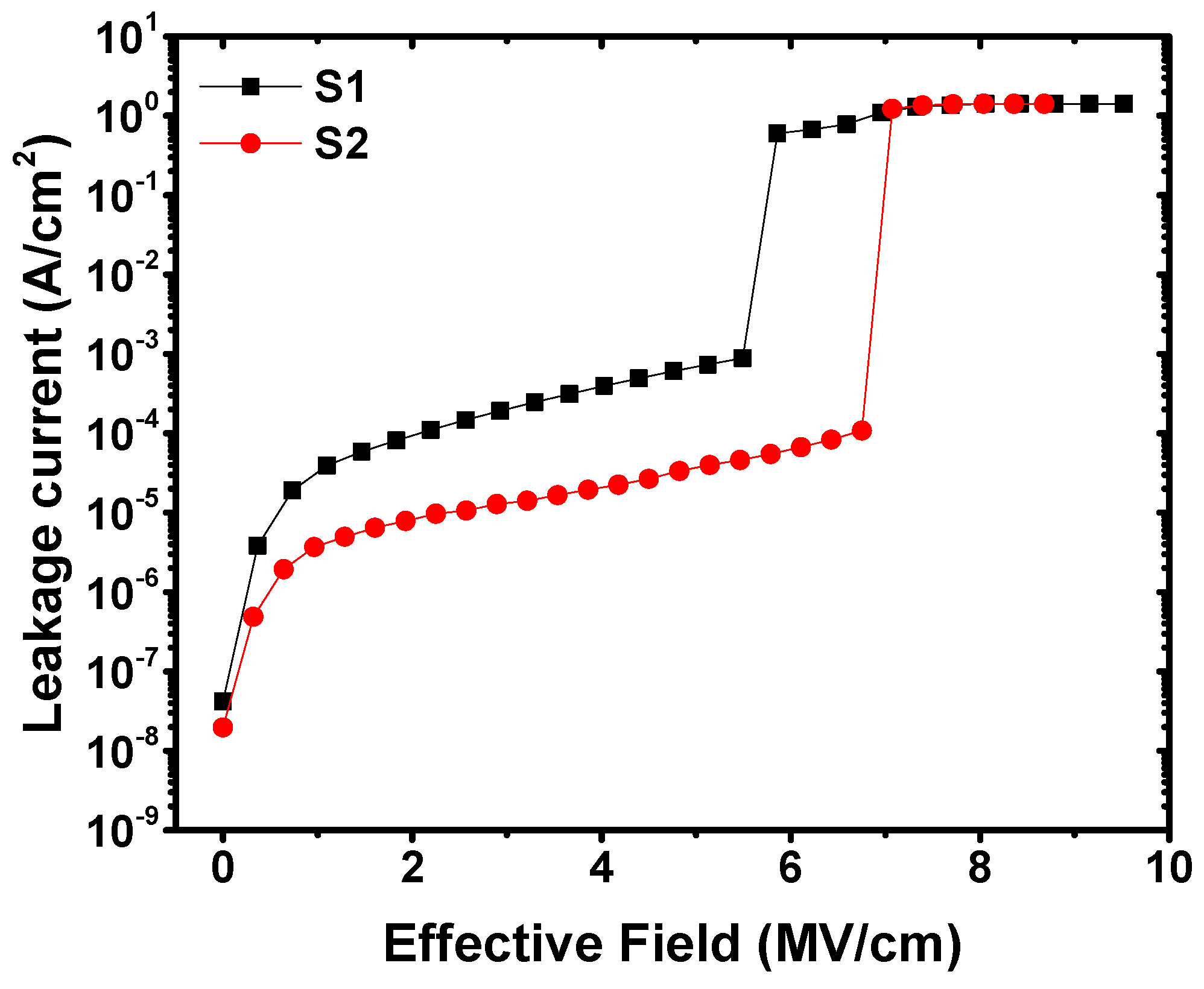
Figure 5 shows the gate leakage current density of the fabricated MIS capacitors as a function of the gate-applied electrical field. The gate leakage current density for capacitors S1 and S2 were measured to be 1.92 × 10⁻⁴ and 1.29 × 10⁻⁵ A/cm2 separately, when the gate-applied electrical field was 3 MV/cm. More than one order of magnitude decrease in the gate leakage current density was achieved after inserting a La2O3 passivation layer. Furthermore, it is worth noting that the gate insulator breakdown electric field of capacitor S2 (~7.07 MV/cm) was apparently higher than that of capacitor S1 (~5.86 MV/cm), which revealed that the inserted La2O3 passivation layer had a positive effect on the breakdown characteristics of the gate insulators. The improvements in gate leakage current density and gate insulator breakdown characteristics were suspected to benefit from the reduction of structural defects including dangling bonds and oxygen vacancies [37]. For the sample with a La2O3 passivation layer, less structural defects in the gate insulator meant a smaller possibility of creating a continuous chain connecting the gate electrode to the substrate semiconductor, contributing to the realization of lower gate leakage current density and higher insulator breakdown electric field [38].
4. Conclusions
The Ge surface engineering using La2O3 as a passivation layer was carried out and investigated systematically in this paper. The formation of a thermodynamically stable LaGeOx interfacial layer effectively suppressed the desorption of volatile GeO, resulting in smaller Not and Dit values achieved after the insertion of a La2O3 passivation layer compared with the control sample. These improvements on the interfacial properties significantly weakened the hysteresis in dual-swept C-V curves and frequency dispersion in multi-frequency C-V curves. Besides, the gate leakage current and insulator breakdown characteristics for the MIS structure with La2O3 passivation were also improved.
Author Contributions
L.Z. generated the research idea, analyzed the data, and wrote the paper; L.Z., X.W., and Y.W. carried out the experiments and the measurements; S.W. participated in the discussions; H.L. gave final approval of the version to be published. All authors read and approved the final manuscript.
Funding
The research described in this paper is fully supported by the National Natural Science Foundation of China (Grant No. 61434007), the Foundation for Fundamental Research of China (Grant No. JSZL2016110B003), the Fundamental Research Funds for the Central Universities, and the Innovation Fund of Xidian University.
Conflicts of Interest
The authors declare no conflicts of interest.
References
- Wilk, G.D.; Wallace, R.M.; Anthony, J.M. High-k gate dielectrics: Current status and materials properties considerations. J. Appl. Phys. 2001, 89, 10. [Google Scholar] [CrossRef]
- Lee, B.H.; Oh, J.; Tseng, H.H.; Jammy, R.; Huff, H. Gate stack technology for nanoscale devices. Mater. Today 2006, 9, 32–40. [Google Scholar] [CrossRef]
- Kingon, A.I.; Maria, J.P.; Streiffer, S.K. Alternative dielectrics to silicon dioxide for memory and logic devices. Nature 2000, 406, 1032. [Google Scholar] [CrossRef] [PubMed]
- Dey, S.; Tapily, K.; Consiglio, S.; Clark, R.D.; Wajda, C.S.; Leusink, G.J.; Woll, A.R.; Diebold, A.C. Role of Ge and Si substrates in higher-k tetragonal phase formation and interfacial properties in cyclical atomic layer deposition-anneal Hf1−xZrxO2/Al2O3 thin film stacks. J. Appl. Phys. 2016, 120, 125304. [Google Scholar] [CrossRef]
- Simoen, E.; Mitard, J.; Hellings, G.; Eneman, G.; DeJaeger, B.; Witters, L.; Vincent, B.; Loo, R.; Delabie, A.; Sioncke, S.; et al. Challenges and opportunities in advanced Ge pMOSFETs. Mat. Sci. Semicond. Process. 2012, 15, 588–600. [Google Scholar] [CrossRef]
- Yi, S.H.; Chang-Liao, K.S.; Wu, T.Y.; Hsu, C.W.; Huang, J.Y. High performance Ge pMOSFETs with HfO2/Hf-Cap/GeOx gate stack and suitable post metal annealing treatments. IEEE Electron Device Lett. 2017, 38, 544–547. [Google Scholar] [CrossRef]
- Xie, Q.; Deng, S.; Schaekers, M.; Lin, D.; Caymax, M.; Delabie, A.; Qu, X.P.; Jiang, Y.L.; Deduytsche, D.; Detavernier, C. Germanium surface passivation and atomic layer deposition of high-k dielectrics—A tutorial review on Ge-based MOS capacitors. Semicond. Sci. Technol. 2012, 27, 074012. [Google Scholar] [CrossRef]
- Kamata, Y. High-k/Ge MOSFETs for future nanoelectronics. Mater. Today 2008, 11, 30–38. [Google Scholar] [CrossRef]
- Houssa, M.; Chagarov, E.; Kummel, A. Surface defects and passivation of Ge and III–V interfaces. MRS Bull. 2009, 34, 504–513. [Google Scholar] [CrossRef]
- Seok, T.J.; Cho, Y.J.; Jin, H.S.; Kim, D.H.; Kim, D.W.; Lee, S.M.; Park, J.B.; Won, J.Y.; Kim, S.K.; Hwang, C.S.; et al. High quality interfacial sulfur passivation via H2S pre-deposition annealing for an atomic-layer-deposited HfO2 film on a Ge substrate. J. Mater. Chem. C 2016, 4, 850–856. [Google Scholar] [CrossRef]
- Yoshida, T.; Kato, K.; Shibayama, S.; Sakashita, M.; Taoka, N.; Takeuchi, W.; Nakatsuka, O.; Zaima, S. Interface properties of Al2O3/Ge structures with thin Ge oxide interfacial layer formed by pulsed metal organic chemical vapor deposition. Jpn J. Appl. Phys. 2014, 53, 8S1. [Google Scholar] [CrossRef]
- Bethge, O.; Henkel, C.; Abermann, S.; Pozzovivo, G.; Stoeger-Pollach, M.; Werner, W.S.M.; Smoliner, J.; Bertagnolli, E. Stability of La2O3 and GeO2 passivated Ge surfaces during ALD of ZrO2 high-k dielectric. Appl. Surf. Sci. 2012, 258, 3444–3449. [Google Scholar] [CrossRef]
- Seo, Y.; Lee, T.I.; Chang, M.Y.; Park, B.E.; Wan, S.H.; Kim, H.J.; Yu, H.Y.; Cho, B.J. The impact of an ultrathin Y2O3 layer on GeO2 passivation in Ge MOS gate stacks. IEEE T. Electron. Dev. 2017, 64, 3303–3307. [Google Scholar] [CrossRef]
- Kouda, M.; Suzuki, T.; Kakushima, K.; Ahmet, P.; Iwai, H.; Yasuda, T. Electrical properties of CeO2/La2O3 stacked gate dielectrics fabricated by chemical vapor deposition and atomic layer deposition. Jpn J. Appl. Phys. 2012, 51, 121101. [Google Scholar]
- Lin, C.C.; Wu, Y.H.; Wu, C.Y.; Lee, C.W. Surface passivation of Ge MOS devices by SmGeOx with sub-nm EOT. IEEE Electron Device Lett. 2014, 35, 3. [Google Scholar] [CrossRef]
- Houssa, M.; Pourtois, G.; Caymax, M.; Meuris, M.; Heyns, M.M. First-principles study of the structural and electronic properties of interfaces (M=Al, La, or Hf). Appl. Phys. Lett. 2008, 92, 242101. [Google Scholar] [CrossRef]
- Liu, Q.Y.; Fang, Z.B.; Liu, S.Y.; Tan, Y.S.; Chen, J.J. Band offsets of La2O3 films on Ge substrates grown by radio frequency magnetron sputtering. Mater. Lett. 2014, 116, 43–45. [Google Scholar] [CrossRef]
- Abermann, S.; Bethge, O.; Henkel, C.; Bertagnolli, E. Atomic layer deposition of ZrO2/La2O3 high-k dielectrics on germanium reaching 0.5 nm equivalent oxide thickness. Appl. Phys. Lett. 2009, 94, 262904. [Google Scholar] [CrossRef]
- Mitrovic, I.Z.; Althobaiti, M.; Weerakkody, A.D.; Dhanak, V.R.; Linhart, W.M.; Veal, T.D.; Sedghi, N.; Hall, S.; Chalker, P.R.; Tsoutsou, D. Ge interface engineering using ultra-thin La2O3 and Y2O3 films: A study into the effect of deposition temperature. J. Appl. Phys. 2014, 115, 114102. [Google Scholar] [CrossRef]
- Mavrou, G.; Galata, S.; Tsipas, P.; Sotiropoulos, A.; Panayiotatos, Y.; Dimoulas, A.; Evangelou, E.K.; Seo, J.W.; Dieker, C. Electrical properties of La2O3 and HfO2/La2O3 gate dielectrics for germanium metal-oxide-semiconductor devices. J. Appl. Phys. 2008, 103, 014506. [Google Scholar] [CrossRef]
- Schmeisser, D.; Schnell, R.D.; Bogen, A.; Himpsel, F.J.; Rieger, D.; Landgren, G.; Morar, J.F. Surface oxidation states of germanium. Surf. Sci. 1986, 172, 455–465. [Google Scholar] [CrossRef]
- Oh, I.K.; Kim, M.K.; Lee, J.S.; Lee, C.W.; Lansalot-Matras, C.; Noh, W.; Park, J.; Noori, A.; Thompson, D.; Chu, S.; et al. The effect of La2O3-incorporation in HfO2 dielectrics on Ge substrate by atomic layer deposition. Appl. Surf. Sci. 2013, 287, 349–354. [Google Scholar] [CrossRef]
- Molle, A.; Baldovino, S.; Fanciulli, M.; Tsoutsou, D.; Golias, E.; Dimoulas, A. Impact of post deposition annealing in the electrically active traps at the interface between Ge (001) substrates and LaGeOx films grown by molecular beam deposition. J. Appl. Phys. 2011, 110, 084504. [Google Scholar] [CrossRef]
- Henkel, C.; Abermann, S.; Bethge, O.; Pozzovivo, G.; Klang, P.; Reiche, M.; Bertagnolli, E. Ge p-MOSFETs with scaled ALD La2O3/ZrO2 gate dielectrics. IEEE Trans. Electron Devices 2010, 57, 3295–3302. [Google Scholar] [CrossRef]
- Bhaisare, M.; Misra, A.; Kottantharayil, A. Aluminum oxide deposited by pulsed-DC reactive sputtering for crystalline silicon surface passivation. IEEE J. Photovolt. 2013, 3, 930–935. [Google Scholar] [CrossRef]
- Cao, D.; Cheng, X.H.; Jia, T.T.; Xu, D.W.; Wang, Z.J.; Xia, C.; Yu, Y.H. Characterization of HfO2/La2O3 layered stacking deposited on Si substrate. J. Vac. Sci. Technol. B Nanotechnol. Microelectron. 2013, 31, 01A113. [Google Scholar] [CrossRef]
- Scarel, G.; Debernardi, A.; Tsoutsou, D.; Spiga, S.; Capelli, S.C.; Lamagna, L.; Volkos, S.N.; Alia, M.; Fanciulli, M. Vibrational and electrical properties of hexagonal La2O3 films. Appl. Phys. Lett. 2007, 91, 102901. [Google Scholar] [CrossRef]
- Pelloquin, S.; Saint-Girons, G.; Baboux, N.; Albertini, D.; Hourani, W.; Penuelas, J.; Grenet, G.; Plossu, C.; Hollinger, G. LaAlO3/Si capacitors: Comparison of different molecular beam deposition conditions and their impact on electrical properties. J. Appl. Phys. 2013, 113, 034106. [Google Scholar] [CrossRef]
- Kaya, S.; Yilmaz, E. Influences of Co-60 gamma-ray irradiation on electrical characteristics of Al2O3 MOS capacitors. J. Radioanal. Nucl. Chem. 2014, 302, 425–431. [Google Scholar] [CrossRef]
- Hauser, J.R.; Ahmed, K. Characterization of ultra-thin oxides using electrical C-V and I-V measurements. AIP Conf. Proc. 1998, 449, 235. [Google Scholar]
- Kumar, A.; Mondal, S.; Rao, K.S.R.K. Critical investigation of high performance spin-coated high-κ titania thin films based MOS capacitor. J. Mater. Sci. Mater. Electron. 2016, 27, 5264–5270. [Google Scholar] [CrossRef]
- Sze, S.M.; Ng, K.K. Physics of Semiconductor Devices, 3rd ed.; John Wiley & Sons: Hoboken, NJ, USA, 2006. [Google Scholar]
- Suzuki, T.; Kouda, M.; Ahmet, P.; Iwai, H.; Kakushima, K.; Yasuda, T. La2O3 gate insulators prepared by atomic layer deposition: Optimal growth conditions and MgO/La2O3 stacks for improved metal-oxide-semiconductor characteristics. J. Vac. Sci. Technol. A 2012, 30, 051507. [Google Scholar] [CrossRef]
- Hill, W.A.; Coleman, C.C. A single-frequency approximation for interface-state density determination. Solid State Electron. 1980, 23, 987. [Google Scholar] [CrossRef]
- Lei, C.; Wang, C.; Wang, G.; Sun, X.; Li, T.; Liu, L. Dielectric relaxations of LaAlO3 ceramics over broad temperature range. J. Alloy. Compd. 2013, 555, 51. [Google Scholar] [CrossRef]
- Kita, K.; Suzuki, S.; Nomura, H.; Takahashi, T.; Nishimura, T.; Toriumi, A. Direct evidence of GeO volatilization from GeO2/Ge and impact of its suppression on GeO2/Ge metal-insulator-semiconductor characteristics. Jpn J. Appl. Phys. 2008, 47, 2349–2353. [Google Scholar] [CrossRef]
- Spahr, H.; Bülow, T.; Nowak, C.; Hirschberg, F.; Reinker, J.; Hamwi, S.; Johannes, H.H.; Kowalsky, W. Impact of morphological defects on the electrical breakdown of ultra thin atomic layer deposition processed Al2O3 layers. Thin Solid Films 2013, 534, 172–176. [Google Scholar] [CrossRef]
- Jinesh, K.B.; Klootwijk, J.H.; Lamy, Y.; Wolters, R.; Tois, E.; Tuominen, M.; Roozeboom, F.; Besling, W.F.A. Enhanced electrical properties of atomic layer deposited La2O3 thin films with embedded ZrO2 nanocrystals. Appl. Phys. Lett. 2008, 93, 172904. [Google Scholar] [CrossRef]
Figure 1.
Shallow core-level spectra of Ge 3d for the (a) 6-nm Al2O3/Ge structure, and (b) 4-nm Al2O3/2-nm La2O3/Ge structure.
Figure 1.
Shallow core-level spectra of Ge 3d for the (a) 6-nm Al2O3/Ge structure, and (b) 4-nm Al2O3/2-nm La2O3/Ge structure.
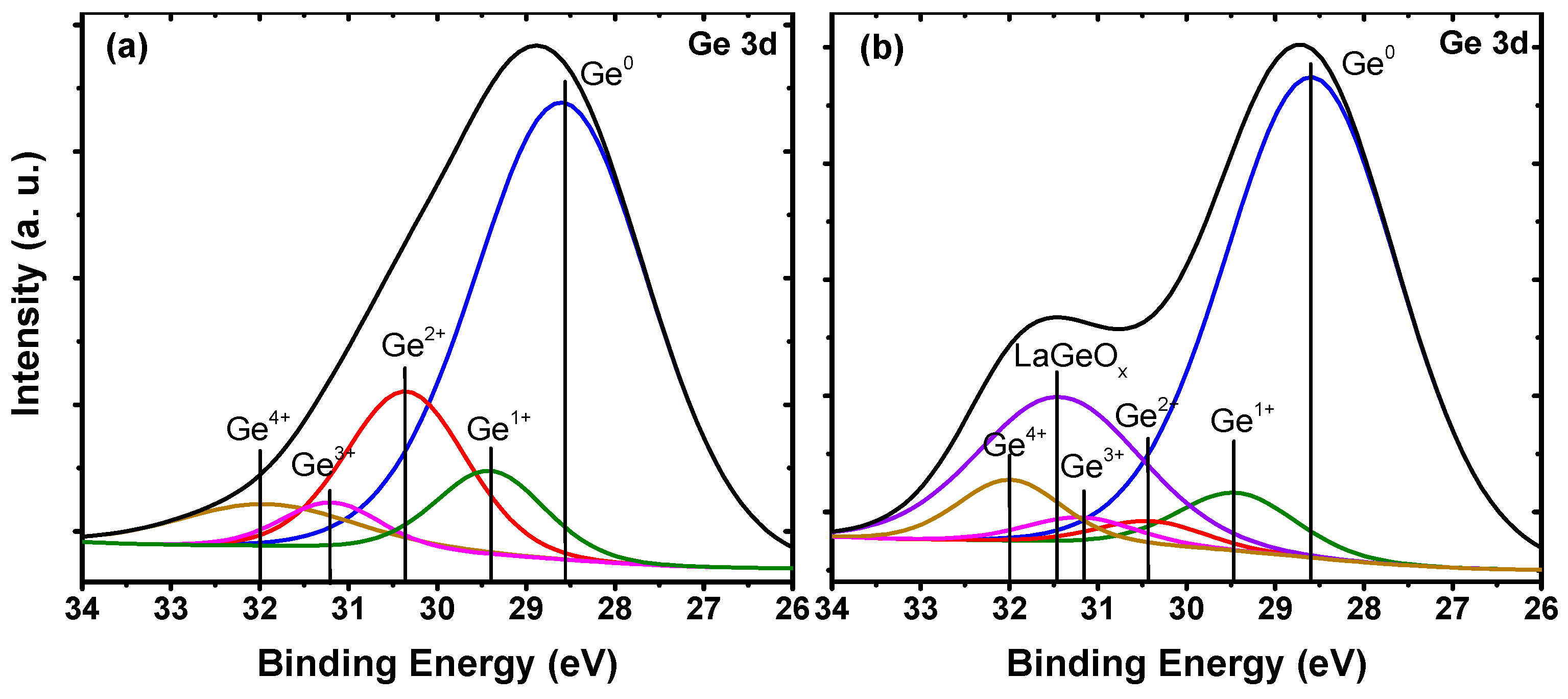
Figure 2.
(a) Two- and (b) three-dimensional AFM images of the Al2O3 films on Ge substrates without La2O3 passivation; and (c) two- and (d) three-dimensional AFM images of the Al2O3 films on Ge substrates with a La2O3 interfacial passivation layer.
Figure 2.
(a) Two- and (b) three-dimensional AFM images of the Al2O3 films on Ge substrates without La2O3 passivation; and (c) two- and (d) three-dimensional AFM images of the Al2O3 films on Ge substrates with a La2O3 interfacial passivation layer.

Figure 3.
C-V characteristics for the fabricated MIS capacitors using Al2O3 films as insulators (a) without and (b) with a La2O3 interfacial passivation layer.
Figure 3.
C-V characteristics for the fabricated MIS capacitors using Al2O3 films as insulators (a) without and (b) with a La2O3 interfacial passivation layer.
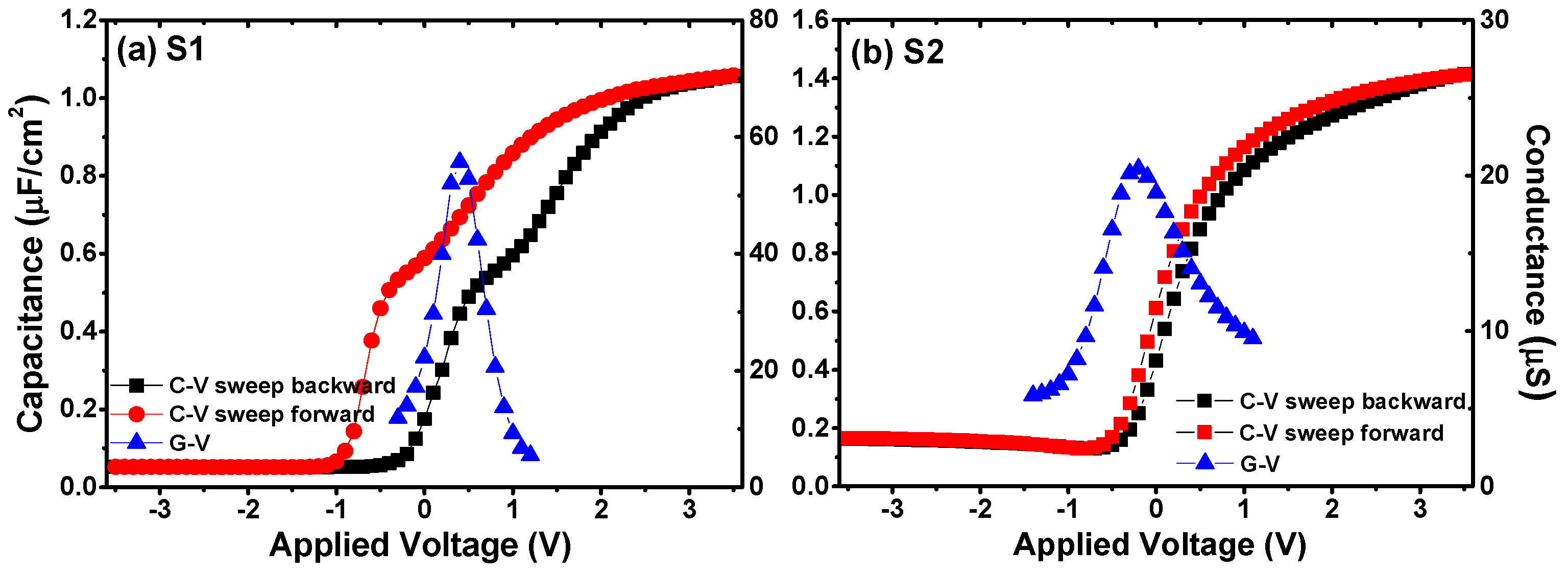
Figure 4.
C-V characteristics measured at various frequencies for the fabricated MIS capacitors using Al2O3 films as insulators (a) without, and (b) with a La2O3 interfacial passivation layer.
Figure 4.
C-V characteristics measured at various frequencies for the fabricated MIS capacitors using Al2O3 films as insulators (a) without, and (b) with a La2O3 interfacial passivation layer.

Figure 5.
J-V characteristics for fabricated MIS capacitors using Al2O3 films as insulators without and with a La2O3 interfacial passivation layer.
Figure 5.
J-V characteristics for fabricated MIS capacitors using Al2O3 films as insulators without and with a La2O3 interfacial passivation layer.


Table 1.
The electrical parameters extracted from the fabricated MIS capacitors without and with a La2O3 interfacial passivation layer.
Table 1.
The electrical parameters extracted from the fabricated MIS capacitors without and with a La2O3 interfacial passivation layer.
| Sample | Cox (µF/cm2) | k | ΔVFB (mV) | Not (cm−2) | Dit (eV−1·cm−2) |
|---|---|---|---|---|---|
| S1 | 1.096 | 7.95 | 863 | 5.91 × 10¹² | 1.13 × 10¹³ |
| S2 | 1.438 | 11.10 | 174 | 1.56 × 10¹² | 4.97 × 10¹² |
© 2018 by the authors. Licensee MDPI, Basel, Switzerland. This article is an open access article distributed under the terms and conditions of the Creative Commons Attribution (CC BY) license (http://creativecommons.org/licenses/by/4.0/).
Share and Cite
MDPI and ACS Style
Zhao, L.; Liu, H.; Wang, X.; Wang, Y.; Wang, S. Improvements on the Interfacial Properties of High-k/Ge MIS Structures by Inserting a La2O3 Passivation Layer. Materials 2018, 11, 2333. https://doi.org/10.3390/ma11112333
AMA Style
Zhao L, Liu H, Wang X, Wang Y, Wang S. Improvements on the Interfacial Properties of High-k/Ge MIS Structures by Inserting a La2O3 Passivation Layer. Materials. 2018; 11(11):2333. https://doi.org/10.3390/ma11112333
Chicago/Turabian StyleZhao, Lu, Hongxia Liu, Xing Wang, Yongte Wang, and Shulong Wang. 2018. "Improvements on the Interfacial Properties of High-k/Ge MIS Structures by Inserting a La2O3 Passivation Layer" Materials 11, no. 11: 2333. https://doi.org/10.3390/ma11112333
Note that from the first issue of 2016, this journal uses article numbers instead of page numbers. See further details here.