

Soft Switched Current Fed Dual Active Bridge Isolated Bidirectional Series Resonant DC-DC Converter for Energy Storage Applications


Abstract
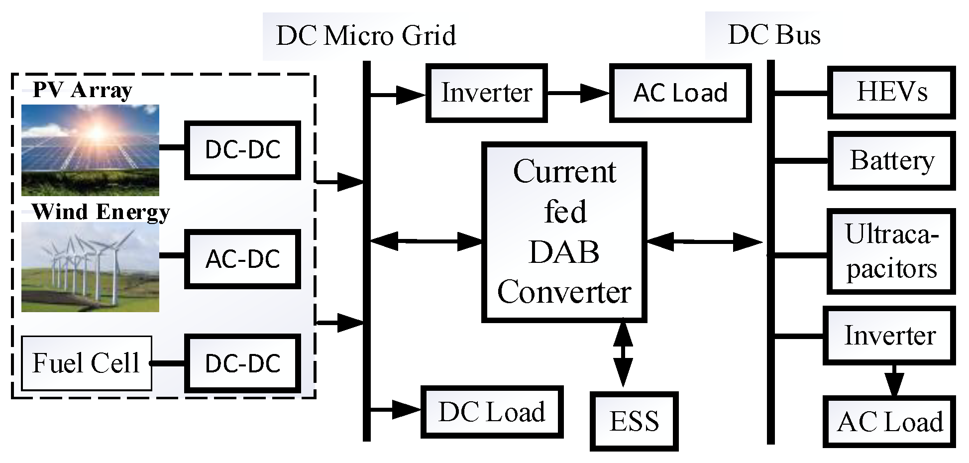
1. Introduction
2. Proposed Circuit: Current-Fed Isolated Dual Active Bridge Bidirectional DC-DC Series Resonant Converter
2.1. Forward Mode of Operation
2.2. Reverse Mode of Operation
3. Steady-State Analysis of the Current-Source IBDC Converter
3.1. Rac for the Inductive Output Filter
3.2. Soft Switching
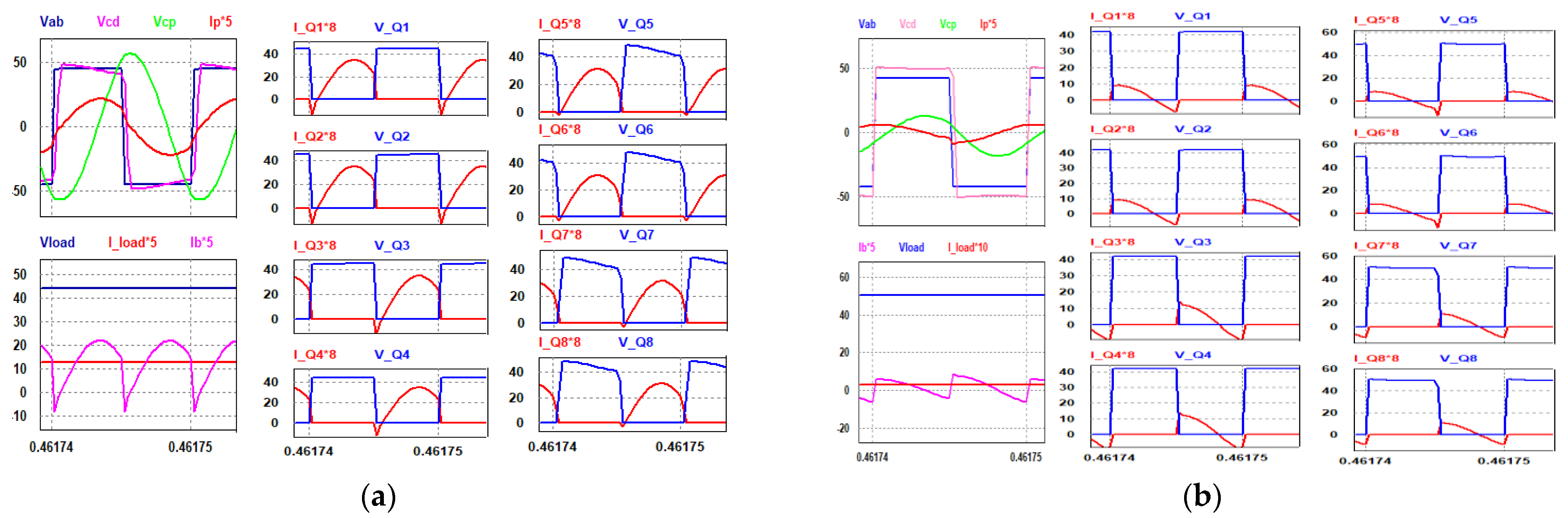
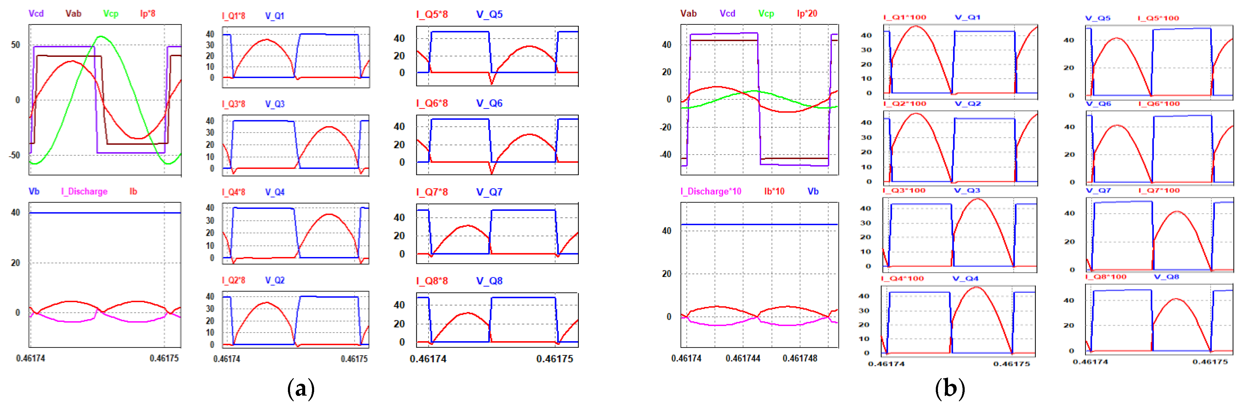
4. Simulation and Experimental Results
4.1. Simulation Results
4.2. Experimental Results
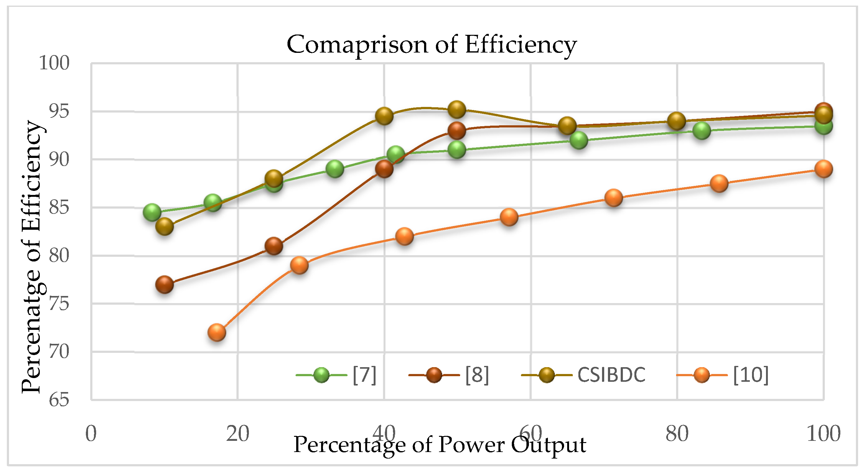
5. Comparison of Results
6. Conclusions
Author Contributions
Funding
Institutional Review Board Statement
Informed Consent Statement
Conflicts of Interest
References
- Kramer, W.; Chakraborty, S.; Kroposki, B.; Thomas, H. Advanced Power Electronic Interfaces for Distributed Energy Systems Part 1: Systems and Topologies; No. NREL/TP-581-42672; National Renewable Energy Lab. (NREL): Golden, CO, USA, 2008. [Google Scholar]
- Lund, H.; Munster, E. Integrated energy systems and local energy markets. Energy Policy. 2006, 34, 1152–1160. [Google Scholar] [CrossRef]
- Chakraborty, S.B.; Kramer, K.W. Advanced Power Electronic Interfaces for Distributed Energy Systems, Part 2: Modeling, Development, and Experimental Evaluation of Advanced Control Functions for Single-Phase Utility-Connected Inverter; No. NREL/TP-550-44313; National Renewable Energy Lab. (NREL): Golden, CO, USA, 2008. [Google Scholar]
- Henao-Bravo, E.E.; Ramos-Paja, C.A.; Saavedra-Montes, A.J.; González-Montoya, D.; Sierra-Pérez, J. Design method of dual active bridge converters for photovoltaic systems with high voltage gain. Energies 2020, 13, 1711. [Google Scholar] [CrossRef]
- Pan, X.; Li, H.; Liu, Y.; Zhao, T.; Ju, C.; Gae, A.K.R. An overview and comprehensive comparative evaluation of current-fed-isolated-bidirectional DC/DC converter. IEEE Trans. Power Electron. 2019, 35, 2737–2763. [Google Scholar] [CrossRef]
- Zhao, B.; Song, Q.; Liu, W.; Sun, Y. Overview of dual-active-bridge isolated bidirectional DC-DC converter for high-frequency-link power-conversion system. IEEE Trans. Power Electron. 2013, 29, 4091–4106. [Google Scholar] [CrossRef]
- Karthikeyan, V.; Gupta, R. Light-load efficiency improvement by extending ZVS range in DAB-bidirectional DC-DC converter for energy storage applications. Energy 2017, 130, 15–21. [Google Scholar] [CrossRef]
- Karthikeyan, V.; Gupta, R. Zero circulating current modulation for isolated bidirectional dual-active-bridge DC-DC converter. IET Power Electron. 2016, 9, 1553–1561. [Google Scholar] [CrossRef]
- Karthikeyan, V.; Gupta, R. FRS-DAB converter for elimination of circulation power flow at input and output ends. IEEE Trans. Ind. Electron. 2017, 65, 2135–2144. [Google Scholar] [CrossRef]
- Prasetya, T.; Wijaya, F.D.; Firmansyah, E. Design of Full-Bridge DC-DC Converter 311/100 V 1kW with PSPWM Method to Get ZVS Condition. Int. J. Power Electron. Drive Syst. 2017, 8, 59. [Google Scholar] [CrossRef]
- Li, X.; Bhat, A.K.S. Analysis and design of high-frequency isolated dual-bridge series resonant DC/DC converter. IEEE Trans. Power Electron. 2009, 25, 850–862. [Google Scholar]
- Bhat, A.K.S.; Zheng, R.L. Analysis and design of a three-phase LCC-type resonant converter. IEEE Trans. Aerosp. Electron. Syst. 1998, 34, 508–519. [Google Scholar] [CrossRef]
- Chen, H.; Bhat, A.K.S. Analysis and design of a dual-bridge series resonant DC-to-DC converter for capacitor semi-active battery-ultracapacitor hybrid storage system. In Proceedings of the 2014 IEEE 23rd International Symposium on Industrial Electronics (ISIE), Istanbul, Turkey, 1–4 June 2014; IEEE: Piscataway, NJ, USA, 2014. [Google Scholar]
- Chen, H.; Bhat, A.K. A bidirectional dual-bridge LCL-type series resonant converter controlled with modified gating scheme. In Proceedings of the 2016 IEEE 8th International Power Electronics and Motion Control Conference (IPEMC-ECCE Asia), Hefei, China, 22–26 May 2016; IEEE: Piscataway, NJ, USA, 2016. [Google Scholar]
- Lee, S.; Hong, W.; Kim, T.; Kim, G.-D.; Lee, E.S.; Lee, S.-H. Voltage balancing control of a series-resonant DAB converter with a virtual line shaft. J. Power Electron. 2022, 22, 1347–1356. [Google Scholar] [CrossRef]
- Yang, J.; Zhang, Y.; Wu, X. Minimum Current Optimization of DBSRC Considering the Dead-Time Effect. Energies 2022, 15, 8484. [Google Scholar] [CrossRef]
- Biswas, M.; Biswas, S.P.; Islam, R.; Rahman, A.; Muttaqi, K.M. A New Transformer-Less Single-Phase Photovoltaic Inverter to Improve the Performance of Grid-Connected Solar Photovoltaic Systems. Energies 2022, 15, 8398. [Google Scholar] [CrossRef]
- Deng, J.; Wang, H. A hybrid-bridge and hybrid modulation-based dual-active-bridge converter adapted to wide voltage range. IEEE J. Emerg. Sel. Top. Power Electron. 2019, 9, 910–920. [Google Scholar] [CrossRef]
- Hebala, O.M.; Aboushady, A.A.; Ahmed, K.H.; Abdelsalam, I.; Burgess, S.J. A New Active Power Controller in Dual Active Bridge DC-DC Converter with a Minimum-Current-Point-Tracking Technique. IEEE J. Emerg. Sel. Top. Power Electron. 2020, 9, 1328–1338. [Google Scholar] [CrossRef]
- Jiang, C.; Liu, H. A novel interleaved parallel bidirectional dual-active-bridge DC-DC converter with coupled inductor for more-electric aircraft. IEEE Trans. Ind. Electron. 2020, 68, 1759–1768. [Google Scholar] [CrossRef]
- Majmunović, B.; Maksimović, D. 400–48-V Stacked Active Bridge Converter. IEEE Trans. Power Electron. 2022, 37, 12017–12029. [Google Scholar] [CrossRef]
- Yamada, R.; Hino, A.; Wada, K. Improvement of Efficiency in Bidirectional DC-DC Converter with Dual Active Bridge Using GaN-HEMT. In Proceedings of the 2022 International Power Electronics Conference (IPEC-Himeji 2022-ECCE Asia), Himeji, Japan, 15–19 May 2022; IEEE: Piscataway, NJ, USA, 2022. [Google Scholar]
- Hou, N.; Zhang, Y.; Li, Y.W. A load-current-estimating scheme with delay compensation for the dual-active-bridge DC-DC converter. IEEE Trans. Power Electron. 2021, 37, 2636–2647. [Google Scholar] [CrossRef]
- Haneda, R.; Akagi, H. Power-Loss Characterization and Reduction of the 750-V 100-KW 16-KHz Dual-Active-Bridge Converter With Buck and Boost Mode. IEEE Trans. Ind. Appl. 2021, 58, 541–553. [Google Scholar] [CrossRef]
- Sha, D.; Wang, X.; Chen, D. High-efficiency current-fed dual active bridge DC-DC converter with ZVS achievement throughout full range of load using optimized switching patterns. IEEE Trans. Power Electron. 2017, 33, 1347–1357. [Google Scholar] [CrossRef]
- Xuewei, P.; Rathore, A.K. Novel interleaved bidirectional snubberless soft-switching current-fed full-bridge voltage doubler for fuel-cell vehicles. IEEE Trans. Power Electron. 2013, 28, 5535–5546. [Google Scholar] [CrossRef]
- Pan, X.; Rathore, A.K. Comparison of bi-directional voltage-fed and current-fed dual active bridge isolated DC-DC converters low voltage high current applications. In Proceedings of the 2014 IEEE 23rd International Symposium on Industrial Electronics (ISIE), Istanbul, Turkey, 1–4 June 2014; pp. 2566–2571. [Google Scholar]
- Bathala, K.; Kishan, D.; Harischandrappa, N. Current Source Isolated Bidirectional Series Resonant DC-DC Converter for Solar Power/Fuel Cell and Energy Storage Application. In Proceedings of the IECON 2021–47th Annual Conference of the IEEE Industrial Electronics Society, Toronto, ON, Canada, 13–16 October 2021; IEEE: Piscataway, NJ, USA, 2021. [Google Scholar]
- Wu, H.; Sun, K.; Li, Y.; Xing, Y. Fixed-frequency PWM-controlled bidirectional current-fed soft-switching series-resonant converter for energy storage applications. IEEE Trans. Ind. Electron. 2017, 64, 6190–6201. [Google Scholar] [CrossRef]
- Wu, H.; Ding, S.; Sun, K.; Zhang, L.; Li, Y.; Xing, Y. Bidirectional soft-switching series-resonant converter with simple PWM control and load-independent voltage-gain characteristics for energy storage system in DC microgrids. IEEE J. Emerg. Sel. Top. Power Electron. 2017, 5, 995–1007. [Google Scholar] [CrossRef]
- Justo, J.J.; Mwasilu, F.; Lee, J.; Jung, J.-W. AC-microgrids versus DC-microgrids with distributed energy resources: A review. Renew. Sustain. Energy Rev. 2013, 24, 387–405. [Google Scholar] [CrossRef]
- Mun, S.-H.; Choi, S.-W.; Hong, D.-Y.; Kong, S.-J.; Lee, J.-Y. Three-phase 11 kW on-board charger with single-phase reverse function. J. Power Electron. 2022, 22, 1255–1264. [Google Scholar] [CrossRef]
- Qin, Z.; Shen, Y.; Loh, P.C.; Wang, H.; Blaabjerg, F. A dual active bridge converter with an extended high-efficiency range by DC blocking capacitor voltage control. IEEE Trans. Power Electron. 2017, 33, 5949–5966. [Google Scholar] [CrossRef]
- Mazumder, S.K.; Rathore, A.K. Primary-side-converter-assisted soft-switching scheme for an AC/AC converter in a cycloconverter-type high-frequency-link inverter. IEEE Trans. Ind. Electron. 2010, 58, 4161–4166. [Google Scholar] [CrossRef]
- Harischandrappa, N. High-Frequency Transformer Isolated Fixed-Frequency DC-DC Resonant Power Converters for Alternative Energy Applications. Ph.D. Thesis, University of Victoria, Victoria BC, Canada, 2015. [Google Scholar]
- Harischandrappa, N.; Bhat, A.K.S. A 10 kW ZVS Integrated Boost Dual Three-Phase Bridge DC-DC Resonant Converter for a Linear Generator-Based Wave-Energy System: Design and Simulation. Electronics 2019, 8, 115. [Google Scholar] [CrossRef]


| Parameter | Specification |
|---|---|
| Output power (Po) | 135 W |
| Output voltage (Vo) | 48 V |
| Switching frequency (fs) | 100 kHz |
| DC Input supply (VPV) | 12–18 V |
| Parameter | Specification |
|---|---|
| Frequency ratio (F) | 1.1 |
| Gain (M) | 0.95 |
| Vo reflected to the primary side () | 42.75 V |
| Transformer turns ratio (1:n) | 1.12 |
| Load resistance (RL) | 13.6 Ω |
| Resonant Inductor (Lr) | 23.8 µH |
| Resonant Capacitor (Cr) | 0.128 µF |
| Impedance (Zab) | 11.02 + j2.52 Ω |
| Peak current (ILr) | 4.71 A |
| Peak voltage (Vcp) | 65.5 V |
| Filter inductance (Lo) | ≤403.4 µH |
| Filter capacitance (Co) | ≥1405 µF |
| Parameter | Forward Mode | Reverse Mode | ||||||||||||||
|---|---|---|---|---|---|---|---|---|---|---|---|---|---|---|---|---|
| Vin(min) = 12 V | Vin(max) = 18 V | V2 = 48 V | ||||||||||||||
| 100% Load | 10% Load | Full Load | 10% Load | Full Load | 10% Load | |||||||||||
| Cal. | Sim. | Expt. | Cal. | Sim. | Expt. | Cal. | Sim. | Cal. | Sim. | Cal. | Sim. | Expt. | Cal. | Sim. | Expt. | |
| Vload(V) | 48 | 44 | 48 | 48 | 49 | 50 | 48 | 44.8 | 48 | 49 | 42.7 | 39.8 | 50 | 42.7 | 43 | 50 |
| Iload(A) | 2.81 | 2.57 | 2.5 | 0.28 | 0.3 | 0.6 | 2.81 | 2.62 | 0.28 | 0.29 | 3.1 | 4.38 | 2.8 | 0.31 | 0.46 | 0.6 |
| Isr,peak | 3.92 | 4.4 | 5 | 1.09 | 1.23 | 0.5 | 3.93 | 4.41 | 1.29 | 1.45 | 3.9 | 4.38 | 5 | 0.41 | 0.46 | 0.5 |
| Vcp | 62.9 | 56.8 | 52 | 5.7 | 12.9 | 14 | 62.9 | 57.1 | 5.7 | 15 | 62.9 | 58 | 55 | 5.7 | 6.29 | 16 |
| δ (o) | 180 | 180 | 170 | 170 | 180 | 170 | 179 | 179 | 165 | 165 | ||||||
| ZVS/ZCS | All | All | All | All | All | All | All | All | All | All | ||||||
| % of Po | [7] | [8] | [10] | CFIBDC |
|---|---|---|---|---|
| 10 | 84.5 | 77.5 | 69 | 83.02 |
| 20 | 86.5 | 79.5 | 74 | 86.5 |
| 30 | 88 | 83.5 | 89.5 | 90 |
| 40 | 90.5 | 89 | 82 | 94.5 |
| 50 | 91 | 92.5 | 83.5 | 95.19 |
| 60 | 91.5 | 92.5 | 84 | 94.3 |
| 70 | 92 | 93 | 86 | 94 |
| 80 | 93 | 93.5 | 87 | 94.2 |
| 90 | 93.2 | 94 | 88 | 94.3 |
| 100 | 93.5 | 95 | 89 | 94.6 |
| % of Po | [7] (Amp) | [8] (Amp) | [10] (Amp) | CFIBDC (Amp) |
|---|---|---|---|---|
| 10 | 2.2 | 0.83 | 0.8 | 1.23 |
| 20 | 2.7 | 1 | 1.5 | 1.42 |
| 30 | 3.7 | 1.3 | 2.3 | 1.6 |
| 40 | - | 1.45 | 3 | 2 |
| 50 | - | 1.67 | 3.4 | 2.33 |
| 60 | - | 1.82 | 3.8 | 2.5 |
| 70 | - | 2.1 | 5 | 2.8 |
| 80 | - | 2.5 | 5.2 | 3.2 |
| 90 | - | 2.75 | 5.8 | 3.7 |
| 100 | - | 2.83 | 6 | 4.4 |
Disclaimer/Publisher’s Note: The statements, opinions and data contained in all publications are solely those of the individual author(s) and contributor(s) and not of MDPI and/or the editor(s). MDPI and/or the editor(s) disclaim responsibility for any injury to people or property resulting from any ideas, methods, instructions or products referred to in the content. |
© 2022 by the authors. Licensee MDPI, Basel, Switzerland. This article is an open access article distributed under the terms and conditions of the Creative Commons Attribution (CC BY) license (https://creativecommons.org/licenses/by/4.0/).
Share and Cite
Bathala, K.; Kishan, D.; Harischandrappa, N. Soft Switched Current Fed Dual Active Bridge Isolated Bidirectional Series Resonant DC-DC Converter for Energy Storage Applications. Energies 2023, 16, 258. https://doi.org/10.3390/en16010258
Bathala K, Kishan D, Harischandrappa N. Soft Switched Current Fed Dual Active Bridge Isolated Bidirectional Series Resonant DC-DC Converter for Energy Storage Applications. Energies. 2023; 16(1):258. https://doi.org/10.3390/en16010258
Chicago/Turabian StyleBathala, Kiran, Dharavath Kishan, and Nagendrappa Harischandrappa. 2023. "Soft Switched Current Fed Dual Active Bridge Isolated Bidirectional Series Resonant DC-DC Converter for Energy Storage Applications" Energies 16, no. 1: 258. https://doi.org/10.3390/en16010258
APA StyleBathala, K., Kishan, D., & Harischandrappa, N. (2023). Soft Switched Current Fed Dual Active Bridge Isolated Bidirectional Series Resonant DC-DC Converter for Energy Storage Applications. Energies, 16(1), 258. https://doi.org/10.3390/en16010258