Thermal Fatigue Modelling and Simulation of Flip Chip Component Solder Joints under Cyclic Thermal Loading


1
School of Hydraulic, Energy and Power Engineering, Yangzhou University, Yangzhou 225127, Jiangsu, China
2
Key Laboratory of Energy Thermal Conversion and Control of Ministry of Education, School of Energy and Environment, Southeast University, Nanjing 210096, Jiangsu, China
3
Jiangsu Key Laboratory of Micro and Nano Heat Fluid Flow Technology and Energy Application, School of Environmental Science and Engineering, Suzhou University of Science and Technology, Suzhou 215009, Jiangsu, China
*
Author to whom correspondence should be addressed.
Energies 2019, 12(12), 2391; https://doi.org/10.3390/en12122391
Submission received: 29 May 2019
/
Accepted: 19 June 2019
/
Published: 21 June 2019
(This article belongs to the Special Issue Modelling, Simulation and Control of Thermal Energy Systems)
Abstract
:Thermal Fatigue of flip chip component solder joints is widely existing in thermal energy systems, which imposes a great challenge to operational safety. In order to investigate the influential factors, this paper develops a model to analyze thermal fatigue, based on the Darveaux energy method. Under cyclic thermal loading, a theoretical heat transfer and thermal stress model is developed for the flip chip components and the thermal fatigue lives of flip chip component solder joints are analyzed. The model based simulation results show the effects of environmental and power parameters on thermal fatigue life. It is indicated that under cyclic thermal loading, the solder joint with the shortest life in a package of flip chip components is located at the outer corner point of the array. Increment in either power density or ambient temperature or the decrease in either power conversion time or ambient pressure will result in short thermal fatigue lives of the key solder joints in the flip chip components. In addition, thermal fatigue life is more sensitive to power density and ambient temperature than to power conversion time and ambient air pressure.
1. Introduction
With the rapid development of microelectronics, microelectronic devices with variable thermal loads have been extensively used in the thermal energy system [1,2,3], chemical production [4,5,6], biomedical detection [7,8,9], deep space exploration fields [10,11,12], and in microelectromechanical systems (MEMS) [13,14,15,16]. The flip chip technology is widely applied in MEMS, in which solder joints are used as both mechanical supports and interconnections between electronic components [17,18]. However, under cyclic thermal loads, solder joints always tend to fatigue failure resulting from the mismatched thermal expansion of the materials in the solder joints [14,19]. Therefore, the thermal fatigue life of a solder joint under cyclic thermal loads is directly related to the safe operation and reliability of the entire electronic device [20]. In this context, the thermal fatigue mechanism and prediction of thermal fatigue life are essential to the designs and reliabilities of electronic products.
Recently, several theoretical efforts to investigate the thermal fatigue mechanism and predict the thermal fatigue life have been undertaken [21,22]. Cheng et al. [17] examined the reliability of the solder interconnect of an advanced ultrafine-pitch integrated circuit chip through three-dimensional finite element (FE) numerical simulations and experimental tests. Incorporating the fatigue criteria based on energy, Chen et al. [23] conducted the improvement of the geometric simplification methods. The accuracy of simulation results depends on the parameters of the local model, including the mesh density, step size, as well as cut boundaries. Jiang et al. [24] compared the prediction results of the fatigue life solder balls in ball grid array (BGA) packaging obtained by the Darveaux model and the Coffin–Manson model, which are energy-based and strain-based, respectively. In either model, the fatigue life increases with height and decreases with diameter. However, the thermal stress distributions for the solder joints in a BGA product is usually nonuniform, which gives rise to uneven thermal fatigue lives for them. It is of significance finding the key solder joint that determines the thermal fatigue life of a BGA product.
In addition, the thermal fatigue life of an electronic device depends on the ambient environment [25,26,27] and cooling condition [28,29]. Considering the environmental conditions of Mars, the reliability of the plastic BGA was experimentally studied under four different thermal cycles (−55 to 100 °C, −55 to 125 °C, −65 to 150 °C, and −120 to 85 °C) [30]. Ghaffarian has taken the optical photomicrographs of BGA to record the progression and characteristics of damage with numerous thermal cycle intervals. Under the thermal cycles with extreme-temperature conditions, the reliabilities of surface-mounted electronic package test boards were assessed for future long-term deep space missions in extreme-temperature environments [31]. The highly accelerated life testing (HALT) technique was applied by Ramesham [32] to assess electronic packaging during long-term deep-space explorations with the extreme temperature ranging from −150 °C to +125 °C in order to achieve optimized design. During this accelerated test within 12 h, an abnormal electrical continuity occurred in the plastic BGA. However, the underlying relationship between the extreme ambient environment and thermal fatigue life of an electronic device is still unclear. In particular, limited attempts have been made to reveal the coupled effects of extreme ambient environments and cyclic thermal loads on thermal fatigue lives.
Although there are several attempts to interpret the thermal fatigue life of an electronic device with the extreme ambient environment via experimental investigations, numerical attempts in exploring the thermal fatigue lives of electronic devices is less available, especially when the electronic devices are operating under low temperature and pressure. Therefore, based on the Darveaux energy method, a theoretical heat transfer and thermal stress model for flip chip components in the cavity of an initial static air flow field and the finite boundary temperature under cyclic thermal loading was developed in an attempt to predict the thermal fatigue lives of flip chip component solder joints. The location of the critical solder joint in a flip chip component with the shortest thermal fatigue life that determines the safety of the entire electronic device is examined. The effects of ambient environment conditions and thermal loads on the thermal fatigue life of the critical solder joint are discussed. This work can provide a further insight into the thermal reliability of an electronic device under extreme ambient environments.
2. Mathematical Model
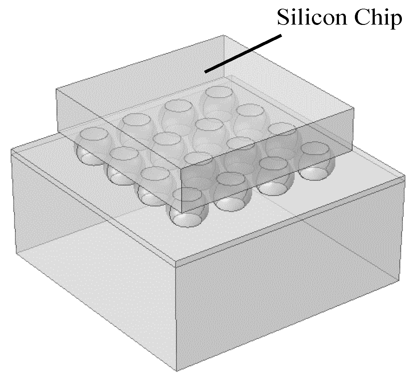
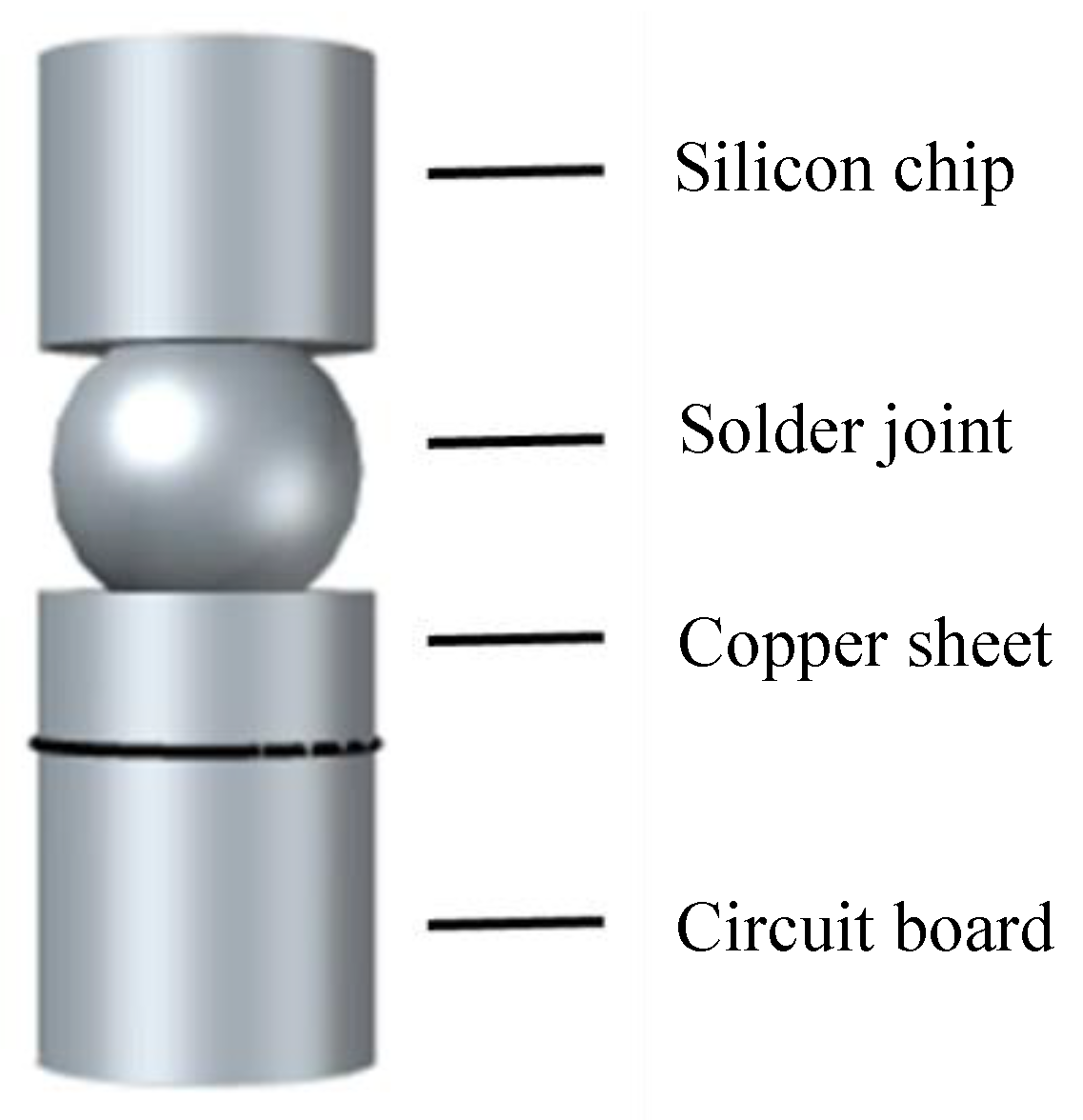
In this paper, a model consist of a 4 × 4 solder joint array of a flip chip component is developed, as shown in Figure 1. The model mainly includes a silicon chip, a circuit board, a copper sheet, and solder joints, as shown in Figure 2. There are 16 solder joints in the 4 × 4 array. Each solder joint has a height of 0.3 mm, a surface area of 4.847 × 10⁻⁷ m2, and a volume of 3.035 × 10⁻¹¹ m3. The shape of the silicon chip is a rectangular parallelepiped with a length of 2 mm, a width of 2 mm, and a height of 0.5 mm. The shape of the copper sheet is a rectangular parallelepiped with a length of 2.7 mm, a width of 2.7 mm, and a height of 0.07 mm. The shape of the circuit board is a rectangular parallelepiped with a length, width and height of 2.7 mm, 2.7 mm, and 1.23 mm, respectively. In this paper, the following assumptions are made: (1) the influences of the printed copper wire, filler and other components on the model are neglected; (2) any residual stress and strain that may occur during the manufacturing process are ignored; (3) the materials in each part are ideally connected; and (4) when the temperature varies, the heat conduction between each kind of material in the model is considered.
2.1. Governing Equations
In this paper, the circuit board, copper sheet, and silicon chip are regarded as isotropic, linear elastic materials. The stress and strain have a simple one-to-one correspondence, and the constitutive equation can be expressed as follows [24]:
where is the stress component, is the elastic stiffness matrix, and is the elastic strain component.
When the ambient temperature of the material is greater than half of its own melting point, viscoplastic behaviors should be considered. Since the mechanical parameters and properties of tin-lead solder are affected by temperature and time, the unified viscoplastic Anand constitutive equation [24] gives the stress-strain response of tin-lead solder under thermal loading.
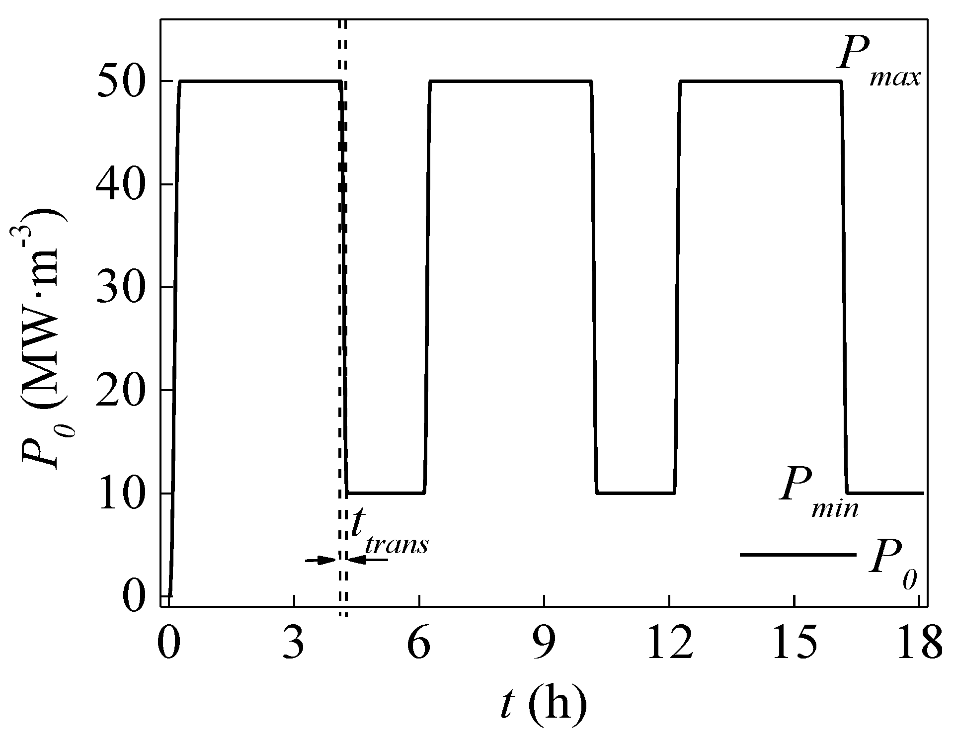
To further study the influence of the working environment of on the thermal fatigue life, the coupled effects of the air flow, thermal convection, heat conduction, and structural mechanics are considered to investigate the thermal characteristics and failure mechanisms of electronic devices in extreme environments. In this paper, cyclic thermal loading of electronic devices is used to simulate the normal working/idle process of an electronic package. In addition, the Darveaux energy method is applied in predicting the thermal fatigue lives. To study the influences of ambient temperature on the thermal fatigue lives of electronic devices, a silicon chip with a cyclic thermal load is considered as a heat source, which conducts heat between each part of the electronic devices. The time-dependent function of the cyclic thermal load is:
where P0 is the power per unit volume of the flip chip component chip heat source. The cyclic thermal load under typical conditions is shown in Figure 3, where the maximum power density of the silicon chip is Pmax = 5 × 10⁷ W·m−3 and the minimum power density is Pmin = 1 × 10⁷ W·m−3. The conversion time of the chip power is ttrans = 600 s.
2.2. Boundary Conditions
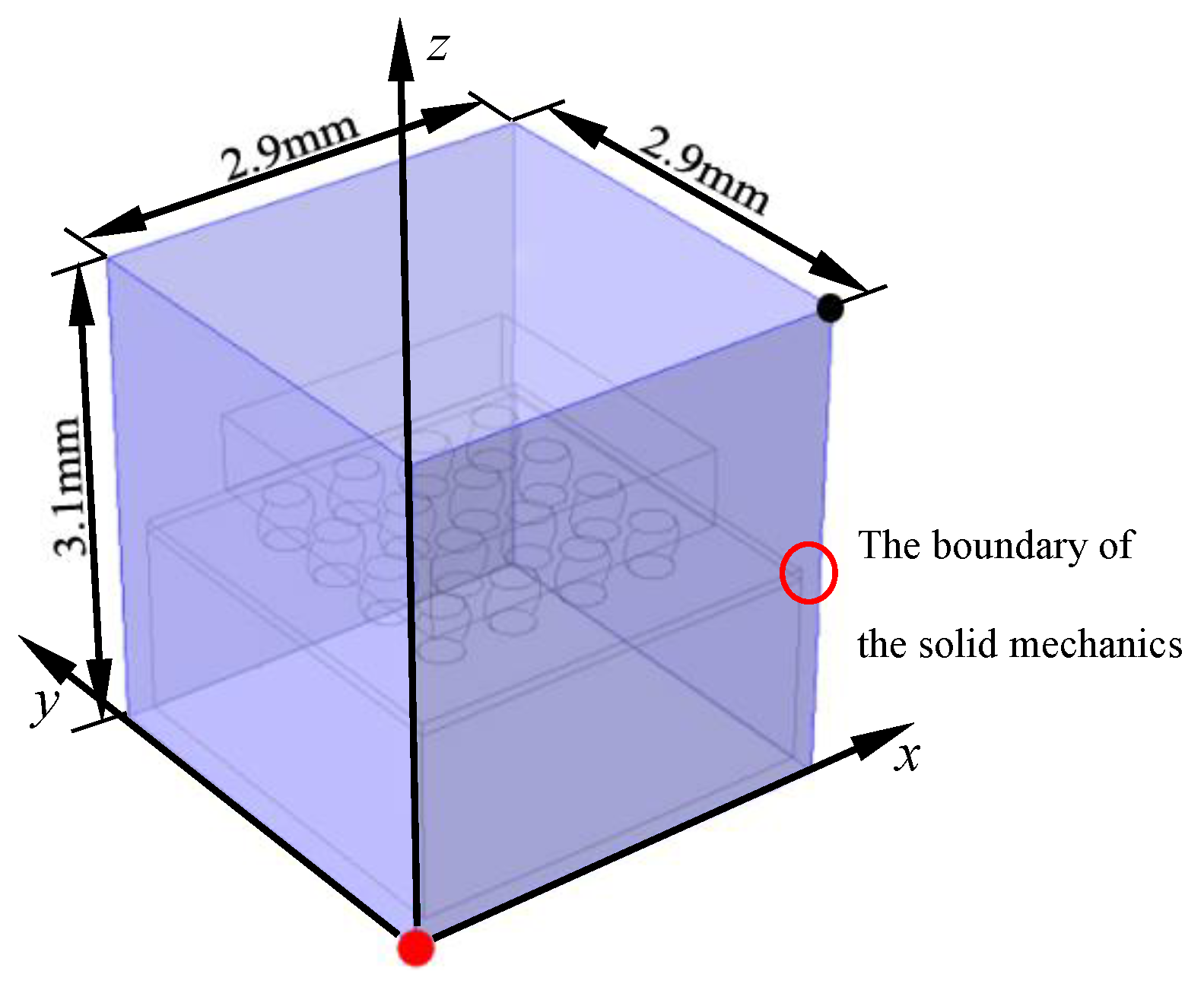
At the beginning of every process, the whole zone of the computational domain is at thermal equilibrium state with a constant temperature and pressure. As shown in Figure 4, the boundaries of the computational domain are assumed to be open faces of constant pressure and temperature through which air can flow, which means the boundaries has the identical temperature and pressure with the ambient. Thus, the boundary conditions of the computational domain can all be written as:
where, the subscripts a and w represent the ambient and the boundaries of computational domain. In this simulation, the ambient temperature and pressure are fluctuant parameters, and the typical ambient temperature and pressure of the whole computational domain is Ta = 20 °C and pa = 1 bar, respectively. Additional, the boundary of the solid mechanics field is set to limit the rigid displacement:
where ω is the displacement of the copper sheet.
The number of breakdown cycles of the electronic component is calculated to predict the thermal fatigue life of the flip chip component. Therefore, the thermal fatigue life of a solder joint in the flip chip component is predicted based on the Darveaux failure model [24].
where N denotes the cyclic number. In this study, the duration of one cycle is 6 h. ΔWave is the increment in the density of average viscoplastic strain energy. ΔWd is the viscoplastic strain energy density increase. and Wd are the strain energy densities of adjacent cycles. and ε are the equivalent strains of adjacent cycles. and σ are the equivalent stresses of adjacent cycles. a = 2.65 × 10⁻⁴ m is the characteristic fracture length, which can be regarded as the diameter of the interface between the solder joint and other materials. K1, K2, K3, and K4 are related physical property parameters, and their specific values are shown in Table 1.
In this paper, a grid independence test is performed by calculating the thermal fatigue lives at different grid numbers. The specific grid data and calculation results are shown in Table 2.
As shown in Table 2, after the number of grids reaches 1 × 10⁶, the predicted thermal fatigue life is basically stable. Considering the calculation accuracy and calculation time, it is suitable to select the calculation grid with a grid number of 1,072,916.
2.3. Model Validation
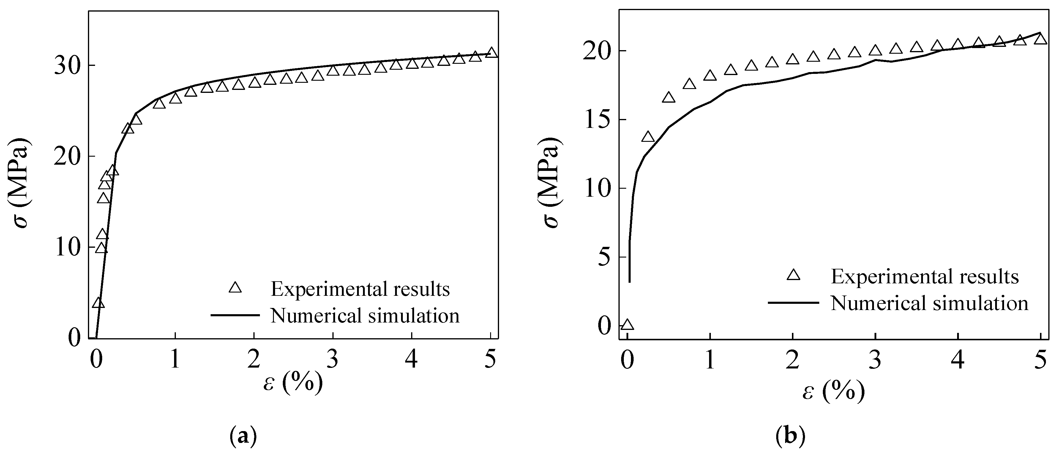
To validate the model, the finite element numerical simulation of the uniaxial tensile test under the two working conditions of 313 K and 353 K is carried out, and the stress parameters are compared with the experimental results from the literature [33], as shown in Figure 5. In the simulations, the strain rate is constant at 0.5% s−1 during uniaxial tensile testing. The two-dimensional geometry of the sample used is illustrated in Figure 5a, and the three-dimensional model is given in Figure 5b. The stress at the tapered collar obtained by the numerical simulation are compared with the experimental results. The mechanical properties of the 63Sn–37Pb solder are shown in Table 3.
Figure 6 shows the good agreement between the numerical simulation and experimental results for the stresses at 313 K and 353 K, which indicates that our model is able to sufficiently describe the mechanical characteristics of the solder at various working temperatures.
3. Results and Discussion
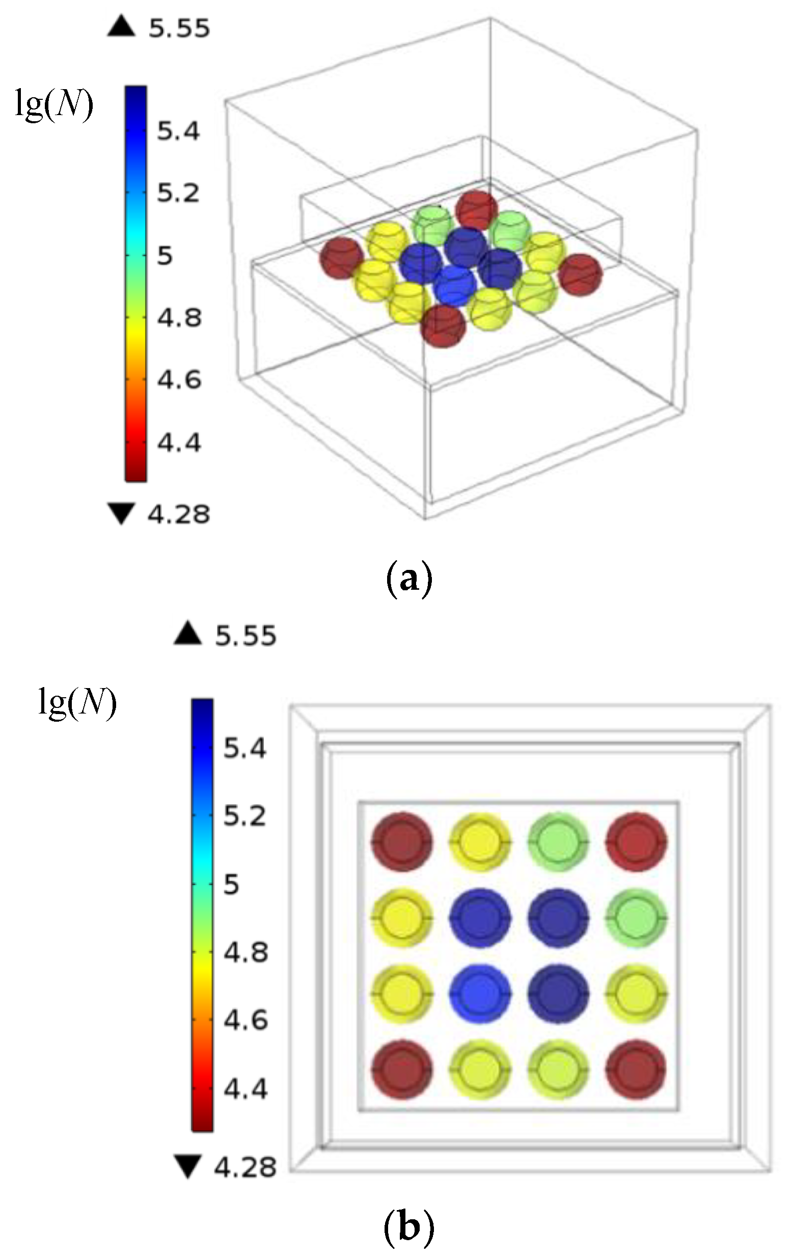
The thermal fatigue life distributions in the flip chip component under typical working conditions is obtained using the Darveaux energy method, where the maximum power density of the silicon chip is Pmax = 5 × 10⁷ W·m−3 and the minimum power density is Pmin = 1 × 10⁷ W·m−3. The conversion time of the chip power is ttrans = 600 s. As illustrated in Figure 7, the solder joint with the shortest thermal fatigue life in the flip chip component appears at the outer corner point, which experience 19,055 (104.28) cycles. Since the malfunction of one solder joint in the flip chip component can lead to the failure of the whole flip chip component, the solder joint with the shortest thermal fatigue life in the flip chip component is regarded as the key solder joint. The thermal fatigue life of this key solder joint is regarded as the final life of the flip chip component under typical conditions. In this paper, the thermal fatigue lives of the flip chip components under various working conditions are investigated, and the dependence of the thermal fatigue life on the maximum power density of the device Pmax and the power conversion time ttrans, ambient temperature T0, ambient pressure p0, and t is analyzed.
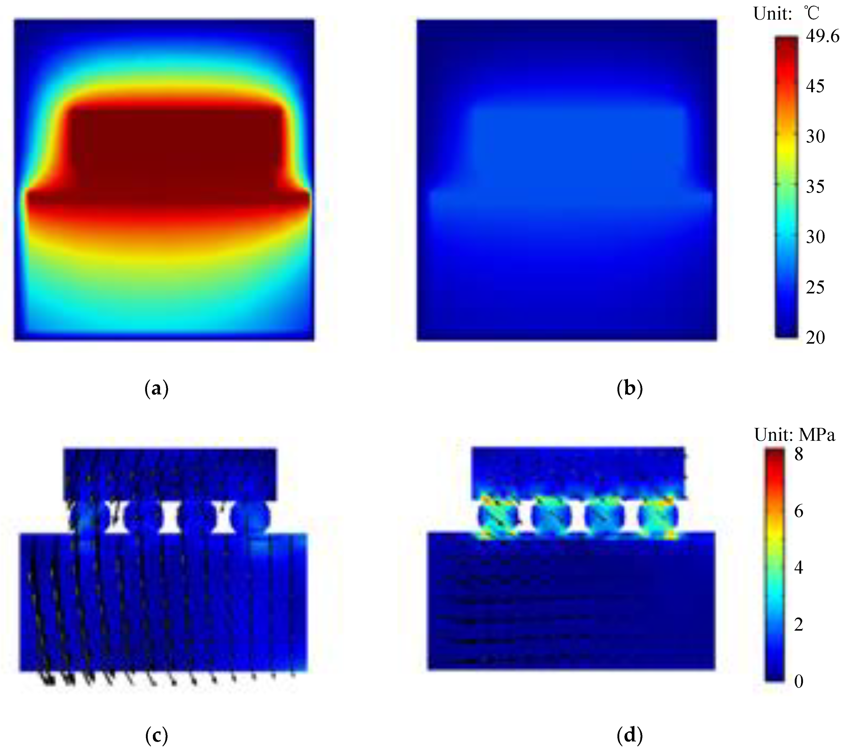
The temperature and stress distribution of the flip chip component is shown in Figure 8. The highest temperature appears at the silicon chip and the solder joint during the high power dissipation period. The stress at the connections between the solder joint and the silicon chip is the maximum. The stress inside the solder joint is much smaller than the stress at the connections.
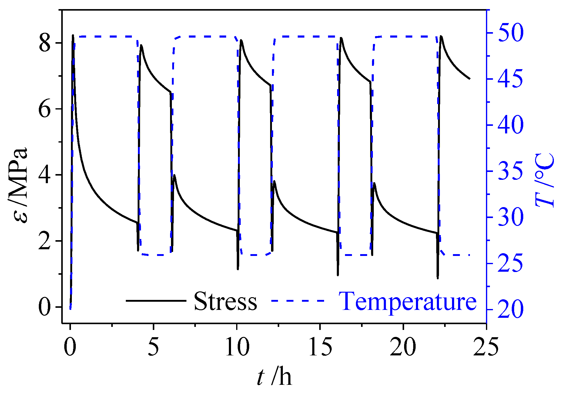
To describe the mechanism that lead to thermal failure of the electronic devices in detail, the evolution of the temperature and the stress data at the connections between the key solder joint and the silicon chip are shown in Figure 9, under the same typical condition in Figure 3. Once the power dissipation transfers from high value to low value or from low value to high value, the variation rate of the temperature at the connection is very high and the stress at the connection suddenly increases. When the temperature of the solder joint is nearly stable, the stress at the connection decreases evidently. The variation of the stress can be attributed to the variation rate of the temperature field, which obviously depends on the maximum heating power and the power conversion time.
3.1. Effects of the Maximum Power Density
The maximum power density Pmax plays a key role in the thermal fatigue lives. To study the effect of Pmax, the parameters of the operating conditions are set as follows:
The other parameters are set to be the same as those under typical operating conditions.
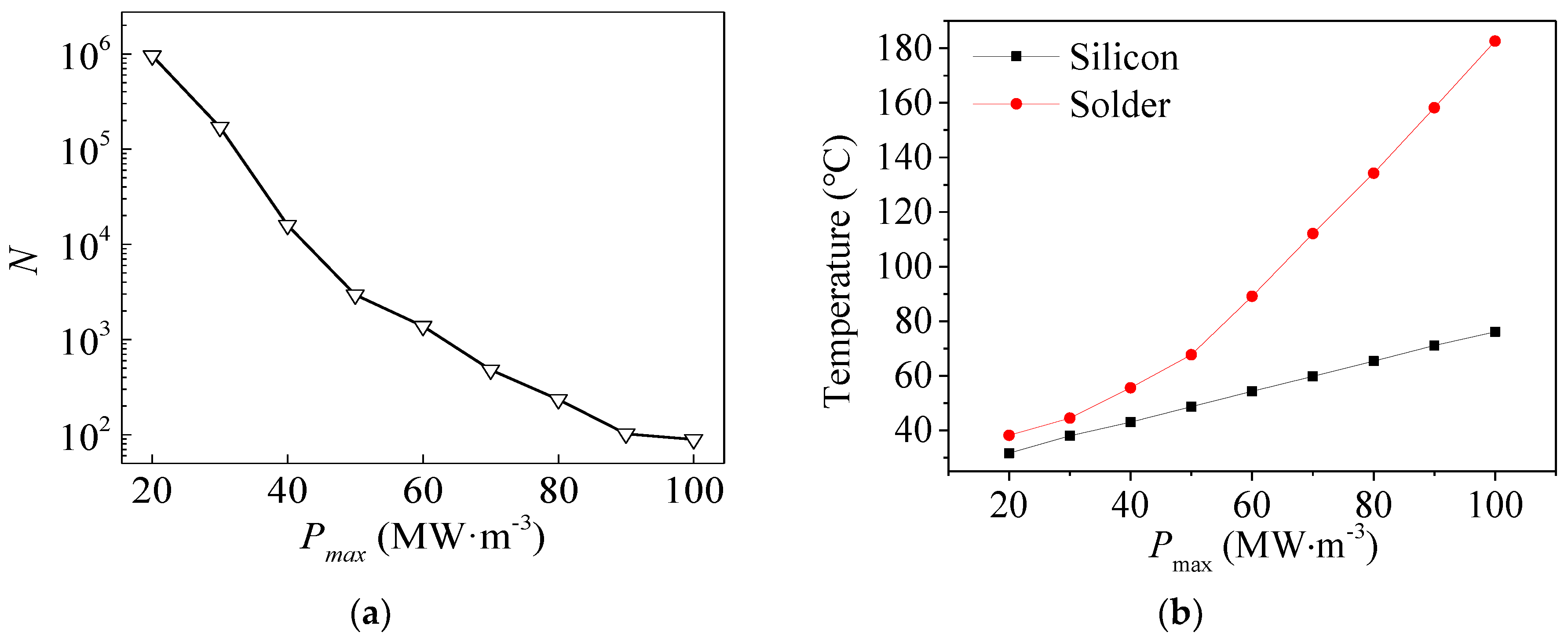
As shown in Figure 10a, when Pmax is less than 50 MW·m−3, the thermal fatigue lives decreases rapidly with Pmax. When Pmax is greater than 50 MW·m−3, the rate of decrease in the thermal fatigue lives in slows down as Pmax increases. In particular, the thermal fatigue lives are reduced to 1/10,730 when Pmax increases from 20 MW·m−3 to 100 MW·m−3 indicating that high heat load is not beneficial for the safe operation. Figure 10b shows that the temperatures of the silicon and solder joint increase with Pmax.
3.2. Effects of the Power Conversion Time
The dependence of thermal fatigue lives on the power conversion time ttrans is analyzed. The parameters of the operating conditions are set as follows:
The other parameters are set to be the same as those under typical operating conditions.
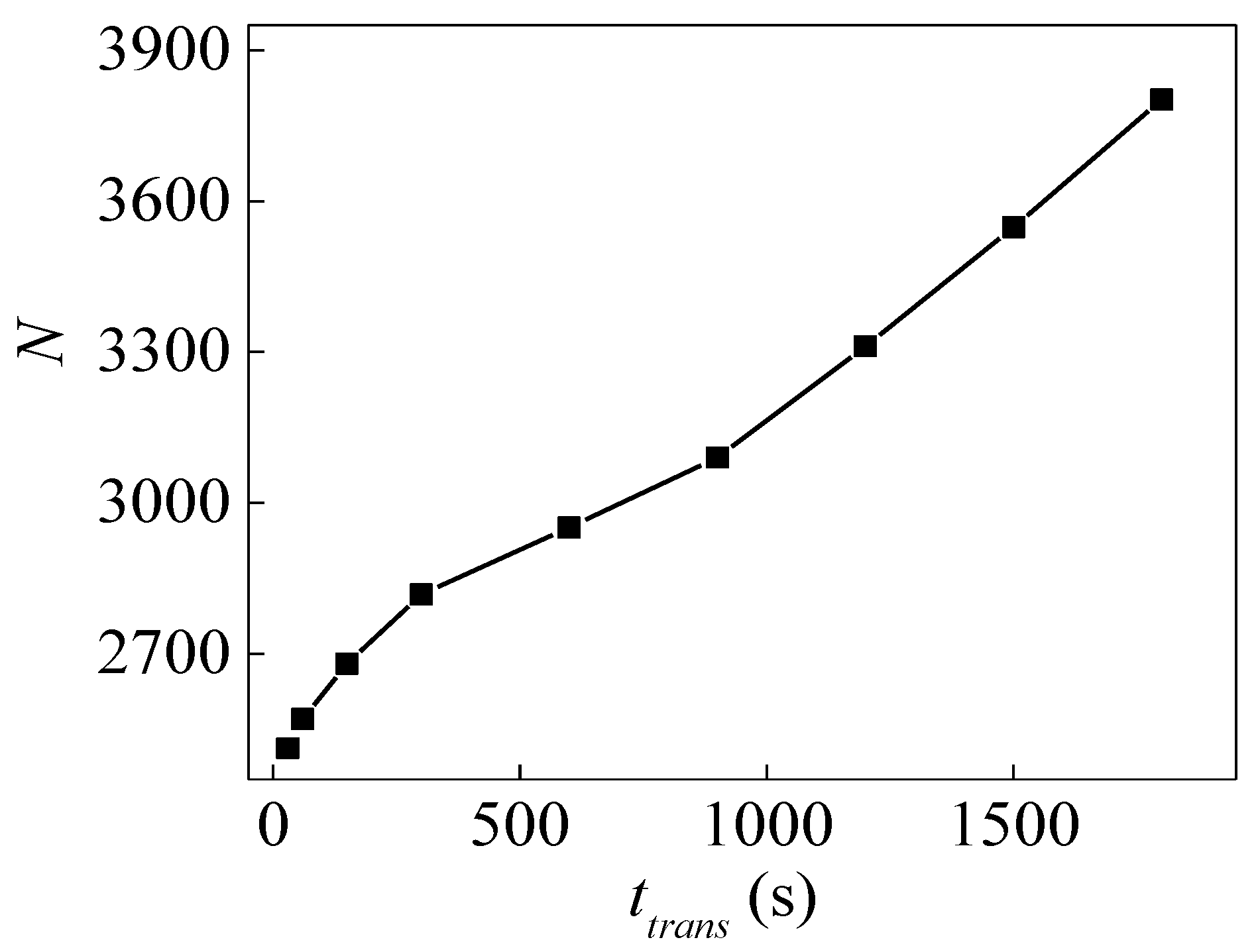
As shown in Figure 11, as ttrans increases, the thermal fatigue lives increase gradually. When ttrans is less than 500 s, the thermal fatigue lives are particularly short, which indicates that the thermal shock generated by the fast conversion from high power to low power bring forth disadvantage in the safe operation of electronic device. Therefore, the conversion rate from high power to low power needs to be carefully controlled.
3.3. Effects of the Ambient Temperature
The temperature difference between flip chip component and the ambient air determines whether the heat can be brought away from the flip chip component. The variation of thermal fatigue lives of the key solder joints versus the ambient air temperature is plotted in Figure 12. The parameters of the operating conditions are set as follows:
The other parameters are set to be the same as those under typical operating conditions.
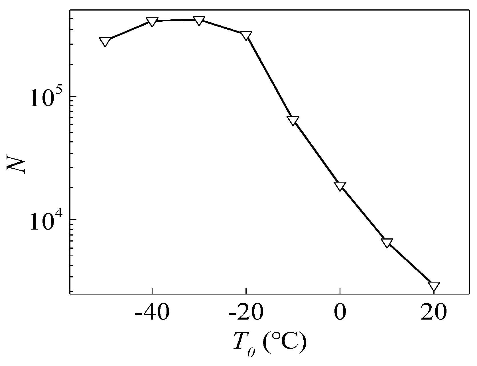
As seen from Figure 12, when the ambient temperature is less than −20 °C, the thermal fatigue lives remain at high values because of the large temperature difference between the key solder joint and ambient environment. These results indicate that the good heat dissipation effect caused by the low ambient temperature can improve the thermal fatigue lives. When the ambient temperature rises and is greater than −20 °C, the heat dissipation is reduced, which leads to a drastic decrement in the thermal fatigue lives. When T0 rises from −20 °C to 20 °C, the thermal fatigue lives are reduced to approximately 1/107. These results show that the working lives of electronic devices decrease with increasing ambient temperature under normal working conditions.
3.4. Effects of the Ambient Pressure
The ambient pressure p0 also have significance during the heat transfer between the flip chip component and the ambient environment as illustrated in Figure 13. The parameters of the operating conditions are set as follows:
The other parameters are set to be the same as those under typical operating conditions.
In Figure 13, as p0 decreases, the thermal fatigue lives gradually decrease. As p0 decreases from 1 bar to 0.1 bar, the thermal fatigue lives decrease by approximately 37.4%. The intermediate temperature of the solder joint at the time t = 7 min increases as the ambient pressure drops. These results indicate that under natural convection conditions, the heat dissipation of an electronic device is weakened by decreases in the ambient air pressure, which leads to quick increases in the temperature and larger stress variation of the solder joint. Therefore, the thermal fatigue life of the key solder joint decreases. For the ambient pressure p0 = 0.05 bar, which is nearly a vacuum environment, the natural convection is extremely weak at this ambient pressure, the heat dissipation of the electronic devices mainly depends on the heat conduction and the heat radiation. So the temperature of the electronic device is relatively high and the thermal fatigue life of the key solder joint is relatively short.
4. Conclusions
In this paper, based on the Darveaux energy method, a theoretical model for BGA products under cyclic thermal loading is developed in an effort to predict the thermal fatigue lives of solder joints in flip chip component. Based on the simulation, the effects of power load factors and environmental factors on thermal fatigue life are analyzed. The main conclusions drawn from the results are as follows:
1. Under the condition of cyclic thermal load, the location of the solder joint with the shortest life in a flip chip component is at the outer corner point in the array. The final life of the flip chip component under typical conditions is equal to the thermal fatigue life of this key solder joint.
2. For the properties of the thermal load, an increase in the power density or a decrease in the power conversion time will result in a short thermal fatigue life of the key solder joint in the flip chip component. Moreover, the thermal shock generated by the fast conversion from high power to low power will have a great disadvantage in the safe operation of the device.
3. When the ambient temperature is lower than −20 °C, the thermal fatigue life of the key solder joint is notably sensitive to the variation in ambient temperature. As a result of the relatively large temperature difference between the ambient environment and the key solder joint, the thermal fatigue life of the key solder joint is high which is beneficial for the reliability of the device. When the ambient temperature rises and is greater than −20 °C, the heat dissipation from the flip chip component to the environment is reduced, which leads to a rapid decrease in the thermal fatigue lives of the key solder joints.
4. Under the condition of natural convection, the heat dissipation of an electronic device is weakened with decreases in the ambient air pressure, which leads to increases in the temperature and failure potential of an electronic device.
Author Contributions
W.Y. provided the guidance and supervision. L.W. and X.H. implemented the main research, discussed the results, and wrote the paper. C.S. and F.Y. collected the data. All authors read and approved the final manuscript.
Funding
The research is financially supported by National Natural Science Foundation of China (Nos. 51706194 and 51876184) and Natural Science Foundation of Yangzhou City (No.YZ2017103).
Conflicts of Interest
The authors declare no conflict of interest.
References
- Sun, L.; Wu, G.; Xue, Y.; Shen, J.; Li, D.; Lee, K.Y. Coordinated control strategies for fuel cell power plant in a microgrid. IEEE Trans. Energy Convers. 2018, 33, 1–9. [Google Scholar] [CrossRef]
- Zhang, C.; Chen, Y.; Wu, R.; Shi, M. Flow boiling in constructal tree-shaped minichannel network. Int. J. Heat Mass Transf. 2011, 54, 202–209. [Google Scholar] [CrossRef]
- Deng, Z.; Liu, X.; Zhang, C.; Huang, Y.; Chen, Y. Melting behaviors of pcm in porous metal foam characterized by fractal geometry. Int. J. Heat Mass Transf. 2017, 113, 1031–1042. [Google Scholar] [CrossRef]
- Chen, Y.P.; Deng, Z.L. Hydrodynamics of a droplet passing through a microfluidic t-junction. J. Fluid Mech. 2017, 819, 401–434. [Google Scholar] [CrossRef]
- Sun, L.; Jin, Y.; Pan, L.; Shen, J.; Lee, K.Y. Efficiency analysis and control of a grid-connected pem fuel cell in distributed generation. Energ. Convers. Manag. 2019, 195, 587–596. [Google Scholar] [CrossRef]
- Graebner, J.; Jin, S.; Kammlott, G.; Bacon, B.; Seibles, L.; Banholzer, W. Anisotropic thermal conductivity in chemical vapor deposition diamond. J. Appl. Phys. 1992, 71, 5353–5356. [Google Scholar] [CrossRef]
- Chen, Y.; Liu, X.; Shi, M. Hydrodynamics of double emulsion droplet in shear flow. Appl. Phys. Lett. 2013, 102, 051609. [Google Scholar] [CrossRef]
- Ghovanloo, M.; Atluri, S. A wide-band power-efficient inductive wireless link for implantable microelectronic devices using multiple carriers. IEEE Trans. Circuits Syst. I Regul. Pap. 2007, 54, 2211–2221. [Google Scholar] [CrossRef]
- Ashraf, M.W.; Tayyaba, S.; Afzulpurkar, N. Micro electromechanical systems (mems) based microfluidic devices for biomedical applications. Int. J. Mol. Sci. 2011, 12, 3648–3704. [Google Scholar] [CrossRef] [PubMed]
- Lupinacci, A.; Shapiro, A.; Suh, J.; Minor, A. A study of solder alloy ductility for cryogenic applications. In Proceedings of the 2013 IEEE International Symposium on Advanced Packaging Materials (APM), Irvine, CA, USA, 27 February–1 March 2013; pp. 82–88. [Google Scholar]
- Liu, X.; Chen, Y.; Shi, M. Dynamic performance analysis on start-up of closed-loop pulsating heat pipes (clphps). Int. J. Therm. Sci. 2013, 65, 224–233. [Google Scholar] [CrossRef]
- Shapiro, A.A.; Tudryn, C.; Schatzel, D.; Tseng, S. Electronic packaging materials for extreme, low temperature, fatigue environments. IEEE Trans. Adv. Packag. 2010, 33, 408–420. [Google Scholar] [CrossRef]
- Niessner, M.; Schuetz, G.; Birzer, C.; Preu, H.; Weiss, L. Accurate prediction of snagcu solder joint fatigue of qfp packages for thermal cycling. In Proceedings of the 2014 15th International Conference on Thermal, Mechanical and Multi-Physics Simulation and Experiments in Microelectronics and Microsystems (Eurosime), Ghent, Belgium, 7–9 April 2014; pp. 1–6. [Google Scholar]
- Li, J.; Karppinen, J.; Laurila, T.; Kivilahti, J.K. Reliability of lead-free solder interconnections in thermal and power cycling tests. IEEE Trans. Compon. Packag. Technol. 2009, 32, 302–308. [Google Scholar]
- Wang, J.; Sun, L.; Zou, M.; Gao, W.; Liu, C.; Shang, L.; Gu, Z.; Zhao, Y. Bioinspired shape-memory graphene film with tunable wettability. Sci. Adv. 2017, 3, e1700004. [Google Scholar] [CrossRef] [PubMed]
- Wang, J.; Gao, W.; Zhang, H.; Zou, M.H.; Chen, Y.P.; Zhao, Y.J. Programmable wettability on photocontrolled graphene film. Sci. Adv. 2018, 4, eaat7392. [Google Scholar] [CrossRef] [PubMed] [Green Version]
- Cheng, H.-C.; Cheng, H.-K.; Lu, S.-T.; Juang, J.-Y.; Chen, W.-H. Drop impact reliability analysis of 3-d chip-on-chip packaging: Numerical modeling and experimental validation. IEEE Trans. Device Mater. Reliab. 2014, 14, 499–511. [Google Scholar] [CrossRef]
- Jen, Y.-M.; Wu, Y.-L.; Fang, C.-K. Impact of the number of chips on the reliability of the solder balls for wire-bonded stacked-chip ball grid array packages. Microelectron. Reliab. 2006, 46, 386–399. [Google Scholar] [CrossRef]
- Perkins, A.; Sitaraman, S.K. Universal fatigue life prediction equation for ceramic ball grid array (cbga) packages. Microelectron. Reliab. 2007, 47, 2260–2274. [Google Scholar] [CrossRef]
- Wu, K.-C.; Lin, S.-Y.; Hung, T.-Y.; Chiang, K.-N. Reliability assessment of packaging solder joints under different thermal cycle loading rates. IEEE Trans. Device Mater. Reliab. 2015, 15, 437–442. [Google Scholar] [CrossRef]
- Jacques, S.; Caldeira, A.; Batut, N.; Schellmanns, A.; Leroy, R.; Gonthier, L. Lifetime prediction modeling of non-insulated to-220ab packages with lead-based solder joints during power cycling. Microelectron. Reliab. 2012, 52, 212–216. [Google Scholar] [CrossRef]
- Che, F.; Pang, J.H. Fatigue reliability analysis of sn–ag–cu solder joints subject to thermal cycling. IEEE Trans. Device Mater. Reliab. 2013, 13, 36–49. [Google Scholar] [CrossRef]
- Chen, C.; Suhling, J.C.; Lall, P. Improved submodeling finite element simulation strategies for bga packages subjected to thermal cycling. In Proceedings of the 2018 17th IEEE Intersociety Conference on Thermal and Thermomechanical Phenomena in Electronic Systems (ITherm), San Diego, CA, USA, 29 May–1 June 2018; pp. 1146–1154. [Google Scholar]
- Jiang, L.; Zhu, W.; He, H. Comparison of darveaux model and coffin-manson model for fatigue life prediction of bga solder joints. In Proceedings of the 2017 18th International Conference on Electronic Packaging Technology (ICEPT), Harbin, China, 16–19 August 2017; pp. 1474–1477. [Google Scholar]
- Ghaffarian, R. Accelerated thermal cycling and failure mechanisms for bga and csp assemblies. J. Electron. Packag. 2000, 122, 335–340. [Google Scholar] [CrossRef]
- Evans, J.W. A Guide to Lead-Free Solders: Physical Metallurgy and Reliability; Springer Science & Business Media: Berlin, Germany, 2007. [Google Scholar]
- Mattila, T.; Xu, H.; Ratia, O.; Paulasto-Kröckel, M. Effects of thermal cycling parameters on lifetimes and failure mechanism of solder interconnections. In Proceedings of the 2010 Proceedings 60th Electronic Components and Technology Conference (ECTC), Las Vegas, NV, USA, 1–4 June 2010; pp. 581–590. [Google Scholar]
- Zhang, C.B.; Chen, Y.P.; Shi, M.H. Effects of roughness elements on laminar flow and heat transfer in microchannels. Chem. Eng. Process. 2010, 49, 1188–1192. [Google Scholar] [CrossRef]
- Zhang, C.B.; Deng, Z.L.; Chen, Y.P. Temperature jump at rough gas-solid interface in couette flow with a rough surface described by cantor fractal. Int. J. Heat Mass Transf. 2014, 70, 322–329. [Google Scholar] [CrossRef]
- Ghaffarian, R. Ccga packages for space applications. Microelectron. Reliab. 2006, 46, 2006–2024. [Google Scholar] [CrossRef]
- Ramesham, R. Reliability of sn/pb and lead-free (snagcu) solders of surface mounted miniaturized passive components for extreme temperature (−185 °C to +125 °C) space missions. In Proceedings of the International Society for Optics and Photonics Reliability, Packaging, Testing, and Characterization of MEMS/MOEMS and Nanodevices X, San Francisco, CA, USA, 11 February 2011; p. 79280F. [Google Scholar]
- Ramesham, R. Halt to qualify electronic packages: A proof of concept. In Proceedings of the International Society for Optics and Photonics Reliability, Packaging, Testing, and Characterization of MOEMS/MEMS, Nanodevices, and Nanomaterials XIII, San Francisco, CA, USA, 3–4 February 2014; p. 89750J. [Google Scholar]
- Zhang, L. Fatigue Life of Bga Composite Solder Joint under Thermal Cycle Loading. Master’s Thesis, Harbin Institute of Technology, Harbin, China, 2011. [Google Scholar]
Figure 1.
Geometry model of a flip chip component.

Figure 2.
Schematic of the flip chip component assembly material.

Figure 3.
Power density of a cyclic thermal load.

Figure 4.
Power density of the cyclic thermal load.

Figure 5.
Uniaxial tensile test finite element numerical calculation model: (a) two-dimensional diagram and (b) three-dimensional diagram.
Figure 5.
Uniaxial tensile test finite element numerical calculation model: (a) two-dimensional diagram and (b) three-dimensional diagram.

Figure 6.
Comparison of the numerical results and experimental data of the 63Sn–37Pb solder: (a) operating temperature of 313 K and (b) operating temperature of 353 K.
Figure 6.
Comparison of the numerical results and experimental data of the 63Sn–37Pb solder: (a) operating temperature of 313 K and (b) operating temperature of 353 K.

Figure 7.
Thermal fatigue life distributions in the flip chip component under typical operating conditions: (a) three-dimensional view and (b) top view.
Figure 7.
Thermal fatigue life distributions in the flip chip component under typical operating conditions: (a) three-dimensional view and (b) top view.

Figure 8.
Temperature and stress distribution of the flip chip component at the vertical section of key solder point: (a) temperature distribution in the high power dissipation period (t = 4.11 h); (b) temperature distribution in the low power dissipation period (t = 6.11 h); (c) stress distribution in the high power dissipation period (t = 4.11 h); and (d) stress distribution in the low power dissipation period (t = 6.11 h).

Figure 9.
Temperature and the stress data at the connections between the key solder joint and the silicon chip. (Pmax = 5 × 10⁷ W·m−3, Pmin = 1 × 10⁷ W·m−3, and ttrans = 600 s).
Figure 9.
Temperature and the stress data at the connections between the key solder joint and the silicon chip. (Pmax = 5 × 10⁷ W·m−3, Pmin = 1 × 10⁷ W·m−3, and ttrans = 600 s).

Figure 10.
Effects of the maximum power density on (a) thermal fatigue lives of the key solder joints and (b) silicon temperatures and maximum of solder temperatures.
Figure 10.
Effects of the maximum power density on (a) thermal fatigue lives of the key solder joints and (b) silicon temperatures and maximum of solder temperatures.

Figure 11.
Effects of the power conversion time on the thermal fatigue lives of the key solder joints.
Figure 11.
Effects of the power conversion time on the thermal fatigue lives of the key solder joints.

Figure 12.
Effects of the ambient temperature on the thermal fatigue lives of the key solder joints.
Figure 12.
Effects of the ambient temperature on the thermal fatigue lives of the key solder joints.

Figure 13.
Effects of the ambient pressure on the thermal fatigue lives of the key solder joints and the maximum temperature of the key solder joints at the time t = 7 min.
Figure 13.
Effects of the ambient pressure on the thermal fatigue lives of the key solder joints and the maximum temperature of the key solder joints at the time t = 7 min.


Table 1.
Material failure parameters.
| Parameter | Value | Description |
|---|---|---|
| K1 | 3.25 cycles∙Pa−1 | Initial crack energy coefficient |
| K2 | −1.52 | Initial crack energy index |
| K3 | 4.04 × 10⁻³ Pa∙cycle−1 | Crack growth energy coefficient |
| K4 | 0.98 | Crack growth energy index |
Table 2.
Computational grid data of the flip chip component model.
| Number of Grids | Thermal Fatigue Life (h) |
|---|---|
| 12981970 | 17484 |
| 2783059 | 17520 |
| 1072916 | 17598 |
| 543249 | 17706 |
| 219631 | 17880 |
| 103691 | 18744 |
| 56625 | 19248 |
| 34138 | 20124 |
Table 3.
Performance parameters of 63Sn–37Pb tin-lead solder at a strain rate of 0.5% s−1.
| Temperature (K) | Elastic Modulus (MPa) |
|---|---|
| 313 | 41350 |
| 353 | 38540 |
| 398 | 34568 |
© 2019 by the authors. Licensee MDPI, Basel, Switzerland. This article is an open access article distributed under the terms and conditions of the Creative Commons Attribution (CC BY) license (http://creativecommons.org/licenses/by/4.0/).
Share and Cite
MDPI and ACS Style
Wu, L.; Han, X.; Shao, C.; Yao, F.; Yang, W. Thermal Fatigue Modelling and Simulation of Flip Chip Component Solder Joints under Cyclic Thermal Loading. Energies 2019, 12, 2391. https://doi.org/10.3390/en12122391
AMA Style
Wu L, Han X, Shao C, Yao F, Yang W. Thermal Fatigue Modelling and Simulation of Flip Chip Component Solder Joints under Cyclic Thermal Loading. Energies. 2019; 12(12):2391. https://doi.org/10.3390/en12122391
Chicago/Turabian StyleWu, Liangyu, Xiaotian Han, Chenxi Shao, Feng Yao, and Weibo Yang. 2019. "Thermal Fatigue Modelling and Simulation of Flip Chip Component Solder Joints under Cyclic Thermal Loading" Energies 12, no. 12: 2391. https://doi.org/10.3390/en12122391
Note that from the first issue of 2016, this journal uses article numbers instead of page numbers. See further details here.