Analysis of LC-LC2 Compensated Inductive Power Transfer for High Efficiency and Load Independent Voltage Gain


1
Power Electronics and Renewable Energy Research Laboratory, Department of Electrical Engineering, University of Malaya, 50603 Kuala Lumpur, Malaysia
2
Center of Excellence in Renewable Energy and Smart Grid, King Abdulaziz University, Jeddah 21589, Saudi Arabia
3
Department of Electrical and Computer Engineering, King Abdulaziz University, Rabigh 21911, Saudi Arabia
4
Department of Electrical and Computer Engineering, King Abdulaziz University, Jeddah 21589, Saudi Arabia
*
Author to whom correspondence should be addressed.
Energies 2018, 11(11), 2883; https://doi.org/10.3390/en11112883
Submission received: 30 June 2018
/
Revised: 20 August 2018
/
Accepted: 27 August 2018
/
Published: 24 October 2018
(This article belongs to the Special Issue Power Electronics for Energy Storage)
Abstract
:A novel LC-LC2 compensated resonant converter topology with high efficiency and good controllable voltage gain is presented in this paper. An additional receiving side inductor working together with the receiving coil has the contribution to work with a large range of air gap distance. Due to this property, proposed compensation technique is effective for IPT based EV charging application. Voltage gain with independent of load and input impedance having ZPA of the proposed resonant converter are observed by the frequency domain analysis. On the other hand, time domain analysis gives the circuit operation. A 500 W LC-LC2 compensated resonant converter prototype is built to testify the theoretical analysis. To observe the efficiency-comparison, an S-SP compensated resonant converter with a similar amount of output power under different air gap is also presented. In order to justify the effectiveness, the proposed compensation method is verified by the laboratory results. The highest efficiency of the proposed compensated resonant converter is 93% with output power of 500 W at 140-mm air gap between the two sides of the IPT (inductive power transfer) transformer.
1. Introduction
Technology of inductive power transfer (IPT) delivers power to the utility load via magnetic coupling, is more suitable and versatile energy transfer method in comparison with traditional methods. Due to the low maintenance cost and highly reliable operation, IPT system is more popular for a large area of applications including battery charging of electric vehicles [1,2,3,4], home appliances [5], biomedical treatments [6,7] and other areas associated with industries [8]. IPT technology normally handles a large variation of loading and magnetic coupling coefficient. In order to achieve maximum efficiency and enhanced controllable output, researcher’s works have been observed on the basis of wide variation of IPT parameters [3,9,10,11,12,13,14,15,16,17,18].
The ruling parameters that affect the efficiency and controllability of output power are: coupling factor and misalignment tolerance. In order to obtain high coupling factor and misalignment tolerance, most of the researchers have focused on the optimization of IPT-parameters [9,19,20]. Another key factor that affects the efficiency and output power controllability of IPT system is the compensation network. Various types of compensation networks by the aid of control technique have been presented and explained in details [16,17,18,21,22,23,24,25,26,27]. Four conventional compensation techniques that are widely used named as S-S (series-series), S-P (series-parallel), P-S (parallel-series), and P-P (parallel-parallel). Among four compensation techniques, P-S and P-P compensated IPT systems are free from danger for the source if the pick-up coil is not present. But these compensation techniques are not suitable to transfer the rated power in case of misalignment condition, as resonant capacitor value strongly depends on the magnetic coupling coefficient and the output load [12]. Consequently, S-S and S-P topologies are widely used in many applications like [10,11,25]. The efficiency of the S-S compensated converter is high when self-inductances of the transmitter and receiver are tuned [10]. Comparison between self-inductance compensation and leakage inductance compensation of S-S topology is presented in [7,25]. However, self-inductance tuned by the S-S compensation presents output voltage which is very sensitive to the output load changes [10]. In order to improve the sensitivity of the output voltage under wide load variation, S-S compensated converter is designed to operate around the frequency of load independent voltage gain [7,25]. On the other hand, input impedance having ZPA is not maintained at a frequency of voltage gain where load is independent. Therefore, efficiency may be lower because of circulating current. In [10], a tradeoff between output voltage controllability and efficiency of the S-S topology is presented. Moreover, the problem still exists as tuning of compensating capacitors is not easy to obtain. Since, S-P compensation provides input impedance with ZPA at a frequency of load independent voltage gain [16]; this technique is suitable for high power applications like [26]. Furthermore, S-P compensation is not effective for a wide range of coupling coefficient and misalignment as load independent voltage gain is inversely related to the coupling coefficient [18]. To maintain a unique output power under the changes of coupling, SP-S compensation network was presented in [17]. There is a large number of research works based on LCL compensation [13,14,15,28]. In [28], a series-parallel LCL tuned unity pick up was presented, that provides uninterrupted power though it reflects reactive power to the source [29]. Another compensation topology with high efficiency named LCC was used in the areas of EV (electric vehicle) charging [23,27]. Here, load independent voltage gain under coupling changes is very much difficult to obtain because of self-coupling between the compensation inductor and main coil. At a frequency of load independent voltage gain, input impedance with ZPA and high power transfer efficiency can be obtained in S-SP compensated resonant converter [18]. Higher-order harmonics are the main limitation of this compensation technique, injected into the rectifier network. These higher order harmonics create the problems for filter design.
A novel LC-LC2 compensation network for IPT system is proposed in this paper which provides input impedance with ZPA and high efficiency at a frequency of load independent voltage gain like S-SP compensated resonant converter. Here, an additional receiving side inductor working parallel to the magnetizing inductance has the great contribution to work under a large range of air gap distance. Because, the parallel effect of additional inductor and magnetizing inductance minimizes the air gap variation effect.
This paper is presented as like: Proposed LC-LC2 compensation is introduced by Section 2. Section 3 provides the frequency domain analysis of the proposed LC-LC2 compensation based resonant converter. Section 4 presents time domain analysis of the proposed LC-LC2 compensation based resonant converter. Section 5 represents the analysis of the experimental results. Finally, Section 6 is summarized.
2. Proposed LC-LC2 Compensation
Analysis of input impedance with ZPA and voltage gain at a frequency where load is independent is described in this section. In this case, T-model for IPT transformer having turn ratio 1: n is chosen. In the T-model, Ll1 and Ll2 depict the leakage inductances of the transmitter and receiver coil of IPT transformer respectively whereas LM is the magnetizing inductance. In case of S-SP compensated resonant converter, Ref. [18] capacitor Cf2 for compensating LM is introduced to the S-S compensated resonant converter. Although input impedance with ZPA and voltage gain with load independent are obtained, higher order harmonics are injected to the rectifier network. To minimize the air gap variation effect as well as the effect of higher order harmonics, an inductor Lf2 parallel with LM is launched to the S-SP compensated resonant converter. In this case, the equivalent parallel inductance of n2LM and Lf2 are compensated by Cf2. This equivalent inductance is expressed as,
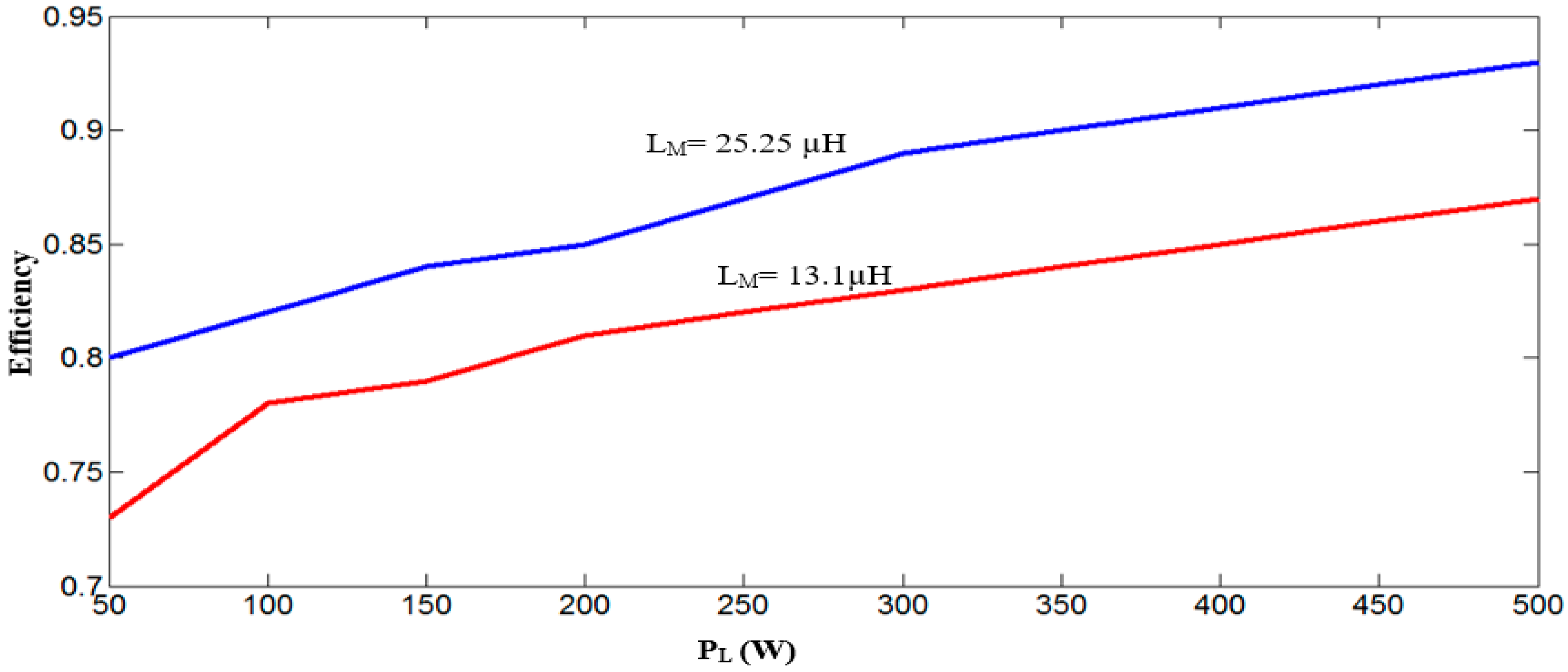
For a resonant frequency, a variation of the air gap (i.e., mutual inductance changes) does not affect the load independent voltage gain and the efficiency so much, because of the parallel effect of Lf2 with LM. This is observed in Figures 6 and 8.
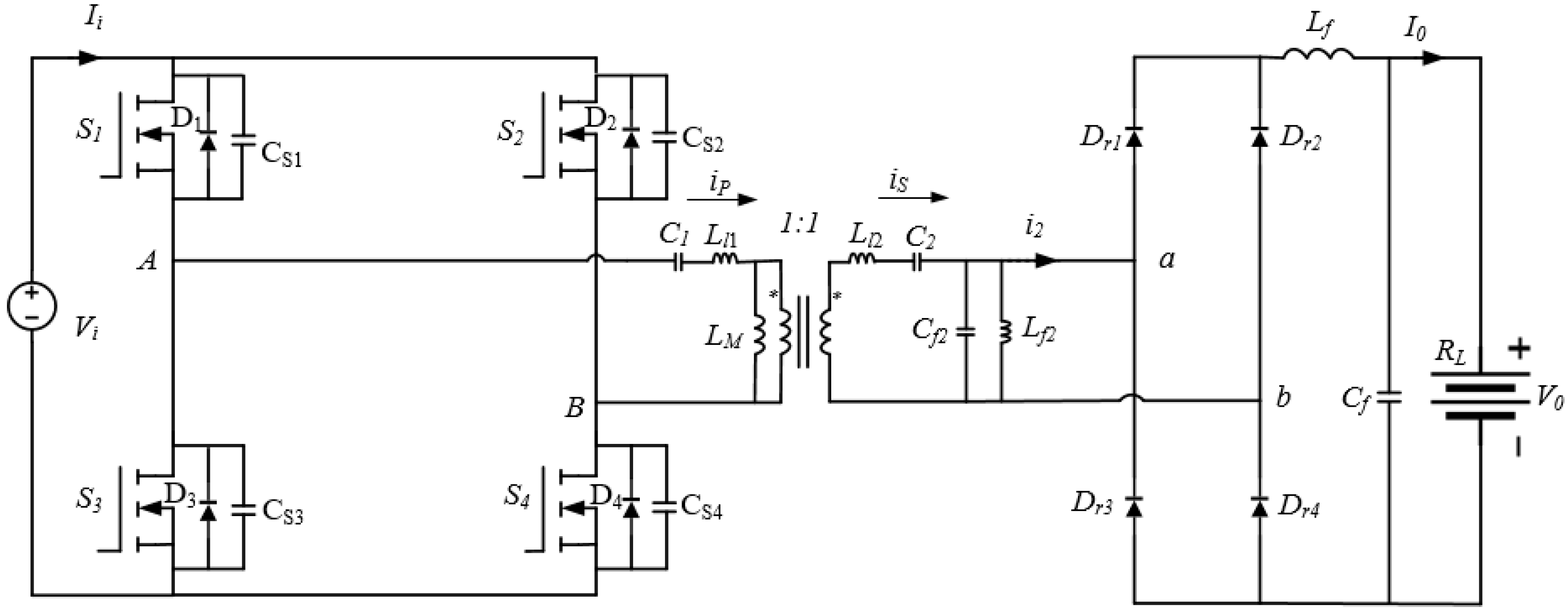
The equivalent circuit of the LC-LC2 compensation network by the help of T-model is depicted in Figure 1. If above equivalent inductance as well as all leakage inductances of the proposed IPT transformer are compensated at a time,
where the resonant frequency is ωr. Ll1, Ll2 and LMf are compensated by C1, C2 and Cf2 respectively.
It can be observed that at the resonant frequency, the output voltage gain of this resonant converter is independent of load and coupling coefficient changes. Also, ZPA of the input impedance is maintained under the full compensation condition.
3. LC-LC2 Compensated Resonant Converter Using Frequency Domain Analysis
In this section, voltage gain with load independence as well as input impedance with ZPA of the proposed LC-LC2 compensated resonant converter have been explained in brief. The proposed LC-LC2 compensated resonant converter is shown in Figure 2.
Here, high frequency inverter is operated by the input dc supply of Vi whereas, V0 is the voltage across the battery having resistance RL. Lf and Cf are used for filtering purpose in order to get pure dc after the high frequency rectifier.
By the help of Kirchhoff’s voltage law, fundamental components of VLM, VAB and Vab can be expressed as,
where = equivalent ac load resistance across the high frequency rectifier side, and .
By the aid of Fourier analysis, the fundamental component of VAB can be depicted as
Due to Lf2, majority portion of higher-order harmonics those are tending to inject into the rectifier, can be eliminated. In later, experimental results of LC-LC2 compensated resonant converter will compare the efficiency with the results of S-SP compensated resonant converter. Furthermore, Vab can be regarded as a sine wave. Therefore, the simplified voltage across the battery can be written as,
From Equations (3)–(6), voltage gain of the LC-LC2 compensated resonant converter can be represented as,
where and
Equation (10) can be expressed as,
From (7), it is observed that voltage gain is not dependent of the load when δ = 0.
Using δ = 0, frequencies at load independent voltage gain are:
where and .
Voltage gain for the above frequencies can be expressed as,
However, frequency at load independent voltage gain is ωr. To obtain a fixed voltage gain at ωr, the subsequent equation should be fulfilled:
By putting and δ = 0 into (16), gives
Therefore, . Substituting into (11), we get
So that, load independent fixed voltage gain with zero effect of coupling factor is obtained when, .
The proposed resonant converter’s input impedance is obtained as,
Substituting into (19), yields
In order to get ZPA of Zi at ωr, the imaginary part must be equal to zero. The input impedance’s imaginary part of (20) can be expressed as,
Under the full compensation, (12) and (13) yields,
Equation (23) follows the Equation (2). Therefore, constant voltage gain and ZPA of input impedance both can be obtained, under the full compensation () condition. This is a desired criterion to get high efficiency and output voltage having good controllability. From (7), the required voltage gain can be obtained as,
That means with the help of the proposed compensation technique, load independent constant voltage gain is achievable which is desirable for IPT based EV application.
4. LC-LC2 Compensated Resonant Converter Using Time Domain Analysis
To explain the time domain analysis, the following hypotheses are made:
- (a)
- All semiconductor switches and diodes are ideal.
- (b)
- Receiver current, iS is almost sinusoidal since proposed converter operates near the resonant frequency.
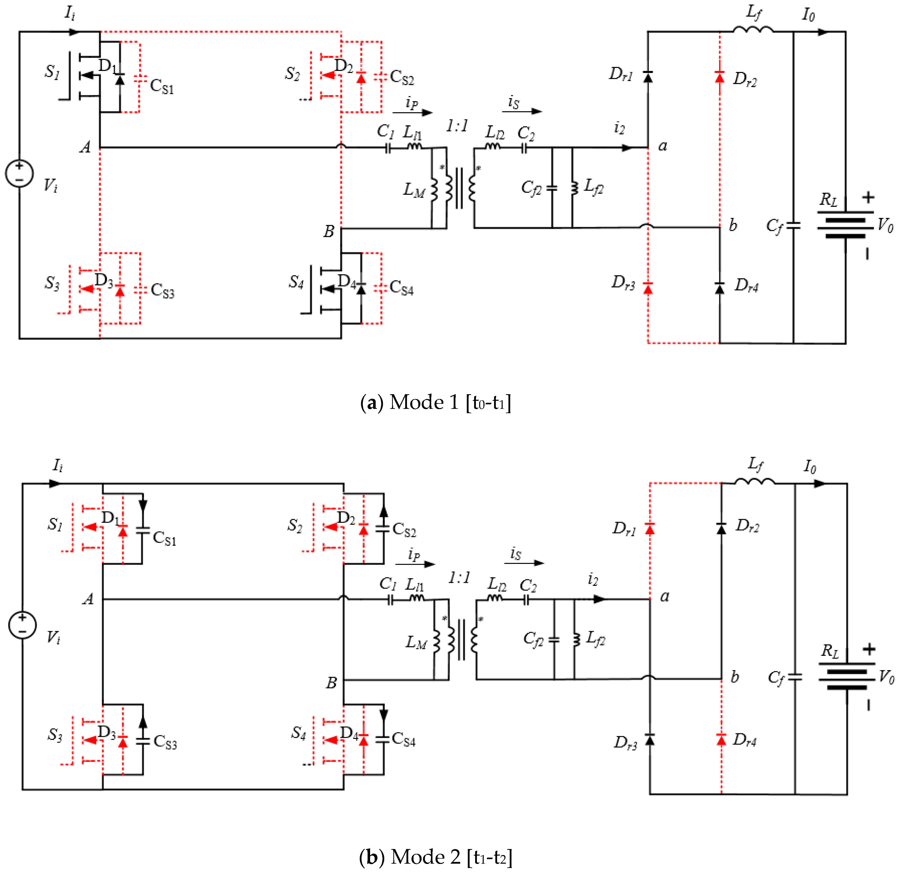
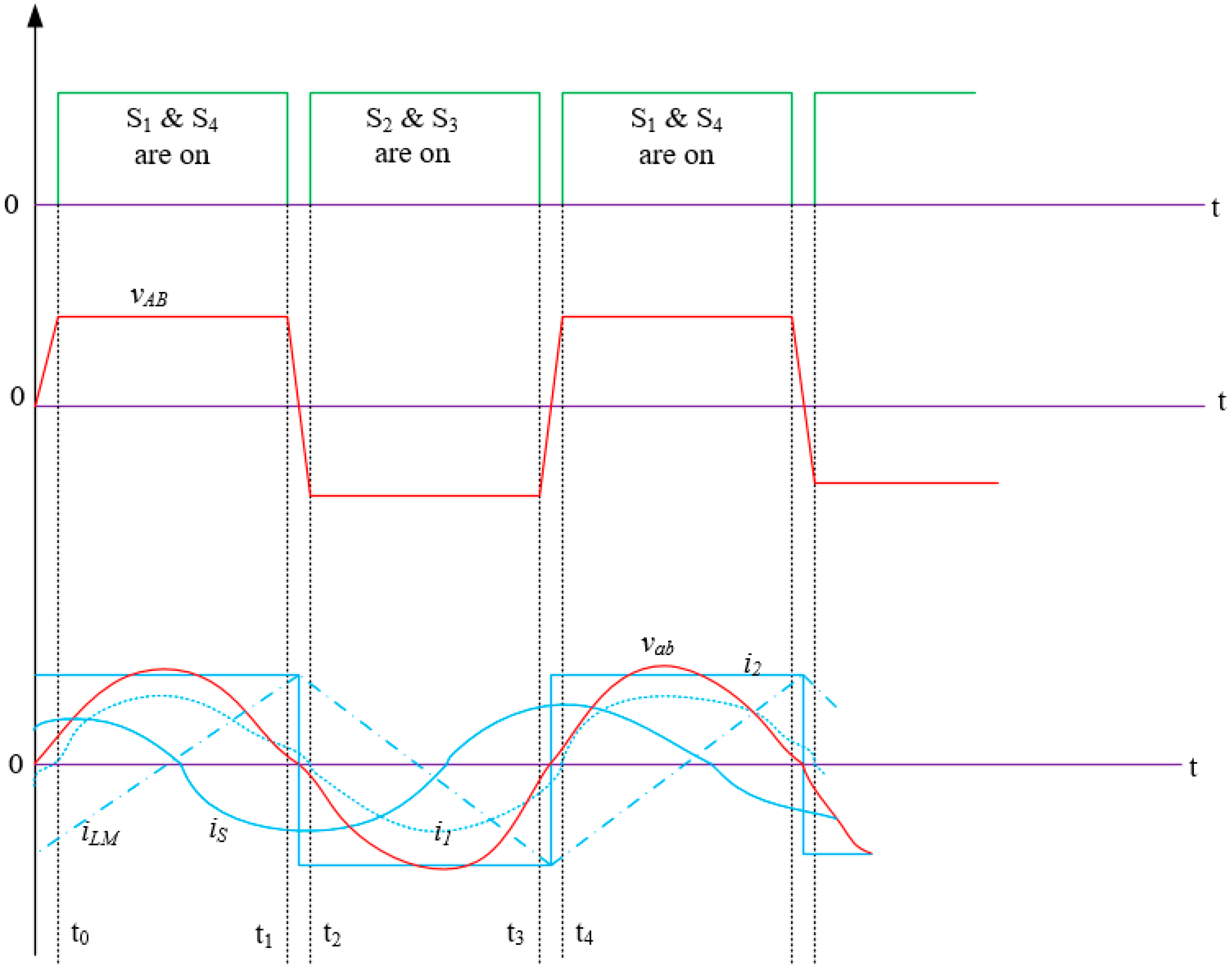
Figure 3a–d depicts the equivalent circuits during different periods of operation of the proposed converter for the operating waveforms shown in Figure 4.
Considering the time instant t0, diagonal switch pair (S1 and S4) of the proposed converter is in conduction and another diagonal switch pair (S2 and S3) is in off mode. At that time VAB is positively equal to Vi. Firstly, transmitter current iP passes through the body diodes of S1 and S4, after that S1 and S4 start to conduct with the changing of current direction. Consequently, ZVS is obtained.
Throughout this period, current flowing into LM can be written as,
where TS is the time period.
Also, receiver current, iS can be obtained as,
Therefore, transmitter current, iP can be calculated as,
Diagonal switch pair (S1 and S4) is in off mode at t1. So that iP charges the CS1 and CS4 and discharges CS2 and CS3. Next, S1 and S4 are turned off at zero voltage as CS1 and CS4 limit the rising voltage rate across the switches. In this case, the direction of iP can be considered as unchanged because of the short duration of this mode. At time instant t2, the voltage across the switches S2 and S3 is fully discharged whereas complete charging of the capacitors of S1 and S4 occurs from 0 to Vi. Then, to maintain the continuity of iP, D2 and D3 start to conduct. So VAB becomes to −Vi.
After the conduction of D2 and D3, diagonal switch pair (S2 and S3) of the proposed converter is in conduction with ZVS. Here, VAB equals to −Vi. During this interval, as like to mode 1 current changes its direction. At first, body diodes of S2 and S3 conduct, after that S2 and S3 start to conduct with the changing of current direction. Throughout this period, current flowing into LM can be written as,
Using (26), transmitter current, iP can be calculated as,
Diagonal switch pair (S2 and S3) is in off mode with ZVS at t3. At time instant t4, the voltage across the switches S1 and S4 is fully discharged whereas complete charging of the capacitors of S2 and S3 occurs from 0 to Vi. Then, to maintain the continuity of iP, D1 and D4 start to conduct. Therefore, ZVS turn on condition occurs for S1 and S4. So, VAB becomes to +Vi.
5. Analysis and Experimental Results
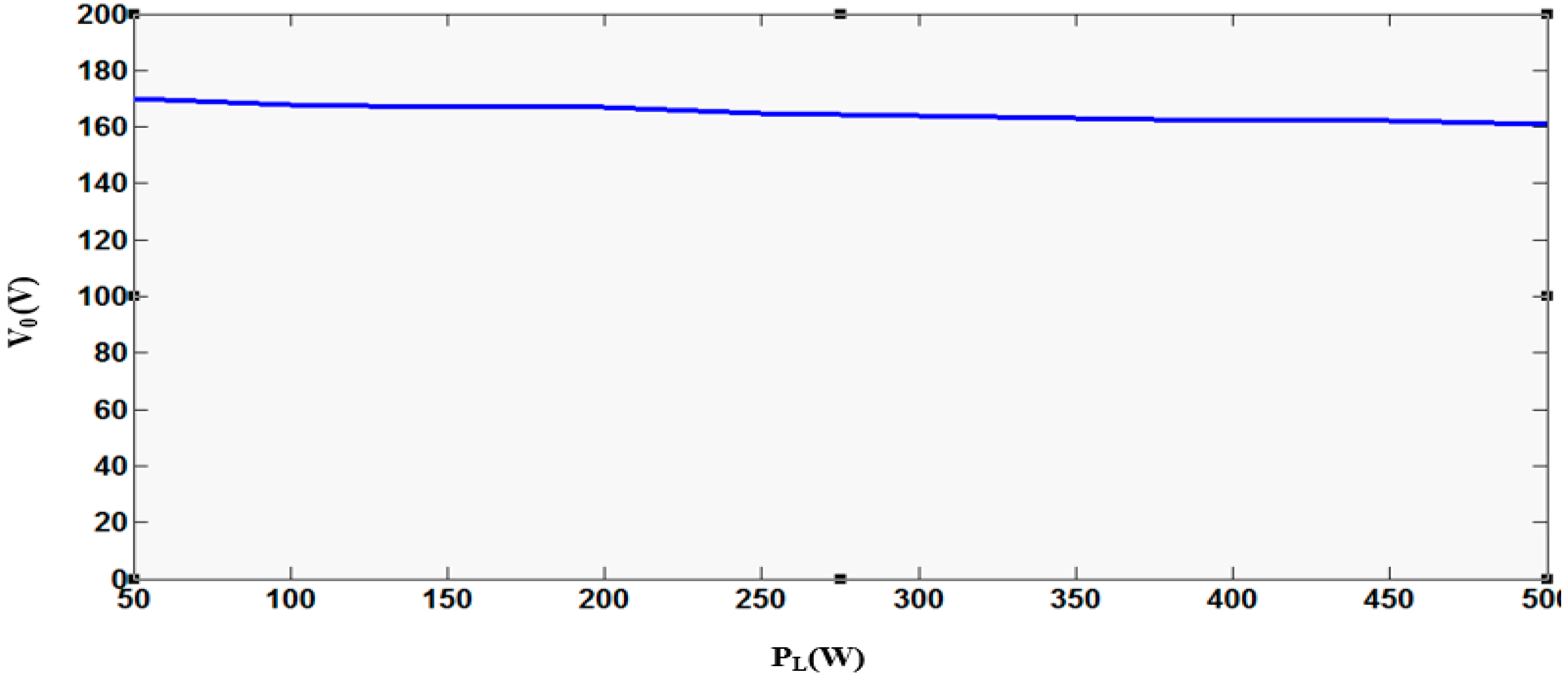
The specifications for 500 W LC-LC2 compensated resonant converter are as follows: Vin = 211 V, V0 = 171 V, P0 = 500 W, an air gap of 140 mm. The loosely coupled transformer with a rectangular shape having I shape ferrite core is used in this resonant converter. Although voltage gain is independent of the mutual inductance, capacitors are designed in case of maximum coupling air gap to make resonance with the corresponding inductances. Therefore, at resonant frequency ZVS can be obtained with the specific frequency control. Detailed specifications of the proposed resonant converter with a constant resonant frequency are shown in Table 1.
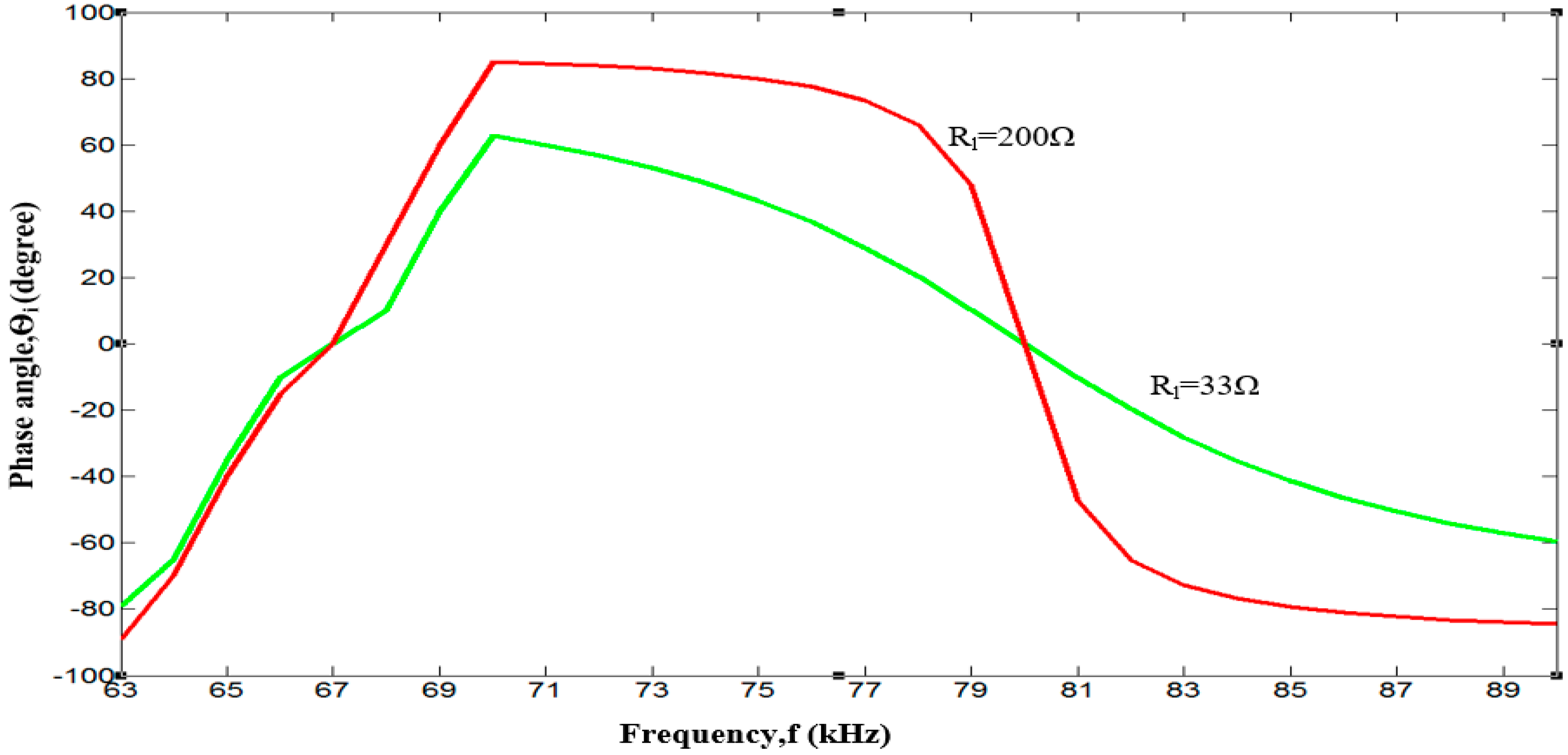
Figure 5 shows that measured phase angle of the input impedance for an air gap of 140 mm with the specifications listed in Table 1. In accordance with the Figure 5, it is observed that load independent input impedance with ZPA is achieved when the proposed converter is totally compensated.
The calculated voltage gain corresponding to the frequency is shown in Figure 6. From Figure 6, load independent voltage gain is found at 80 kHz which follows the Equation (23) as well as Equation (2). Comparing Figure 5 and Figure 6; voltage gain having load independence and input impedance with ZPA, both can be obtained at the frequency of ωH. The load-regulation curve of the proposed LC-LC2 converter from laboratory results is shown in Figure 7.
The experimental efficiency from dc source to the battery is calculated for proposed mutual inductance as well as mutual inductance (13.1 µH) for different air gap of 180 mm.
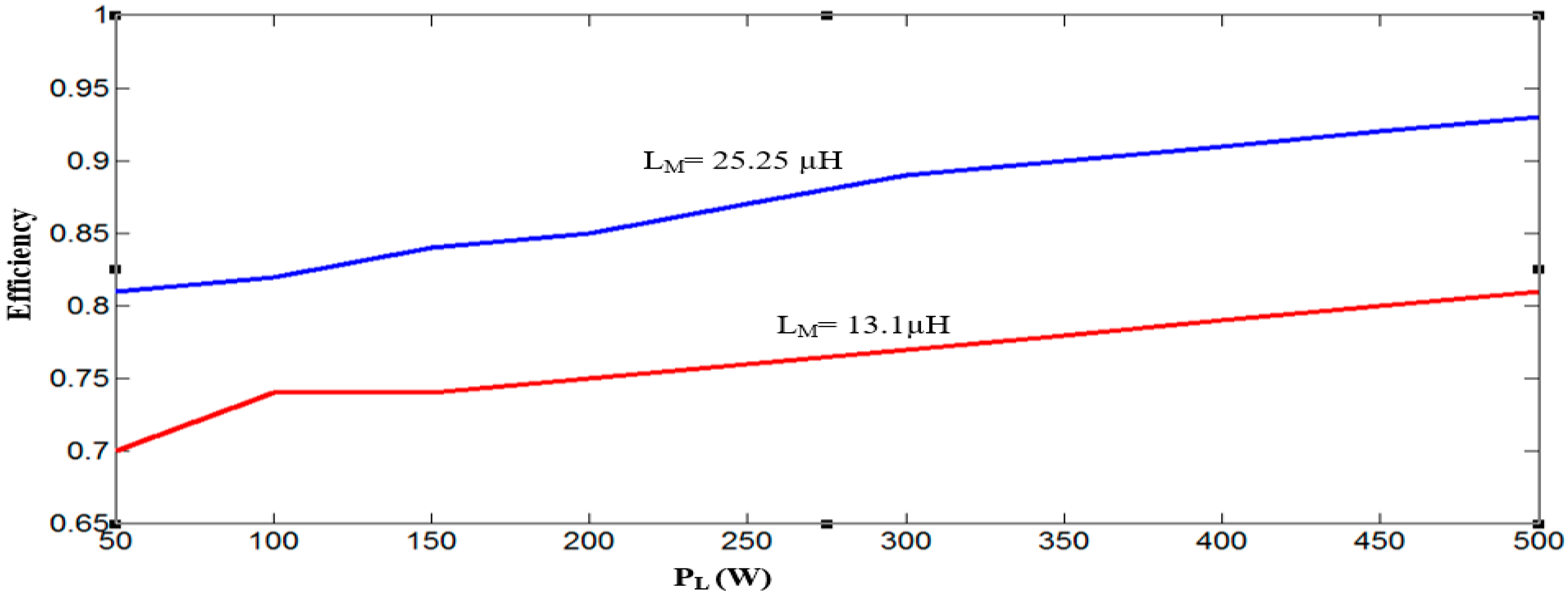
To compare the coupling tolerance of the proposed converter with S-SP compensated resonant converter, the specifications for 500 W S-SP compensated converter are: Vin = 211 V, V0 = 171 V, P0 = 500 W, C1 = 47.71 nF, C2 = 48.24 nF, Cf2 = 156.75 nF, an air gap of 140 mm, RL = 33–200 Ω. In case of S-SP compensated resonant converter, Cf2 compensates the mutual inductance, LM. On the other hand, equivalent inductance is compensated by Cf2 in case of the proposed converter.
Comparing Figure 8 and Figure 9, when the mutual inductance is about 13.1 µH, efficiency is much affected in case of S-SP resonant converter. Because efficiency of the S-SP compensated resonant converter directly related to the mutual inductance whereas efficiency of the LC-LC2 compensated resonant converter related to the equivalent inductance, . Therefore, LC-LC2 compensated resonant converter provides better efficiency than S-SP compensated resonant converter in case of variant air gap condition by which mutual inductance changes. Based on this, it is clear that due to the parallel effect of magnetizing inductance and the additional inductance of the secondary side, phase angle of the input impedance is closely maintained to zero. That’s why efficiency is not so much affected by the air gap variation. Also higher order harmonics of i2 from is are limited. Although the proposed compensation technique is built for 140–180 mm air gap variation, the laboratory setup for 140 mm air gap variation is shown in Figure 10.
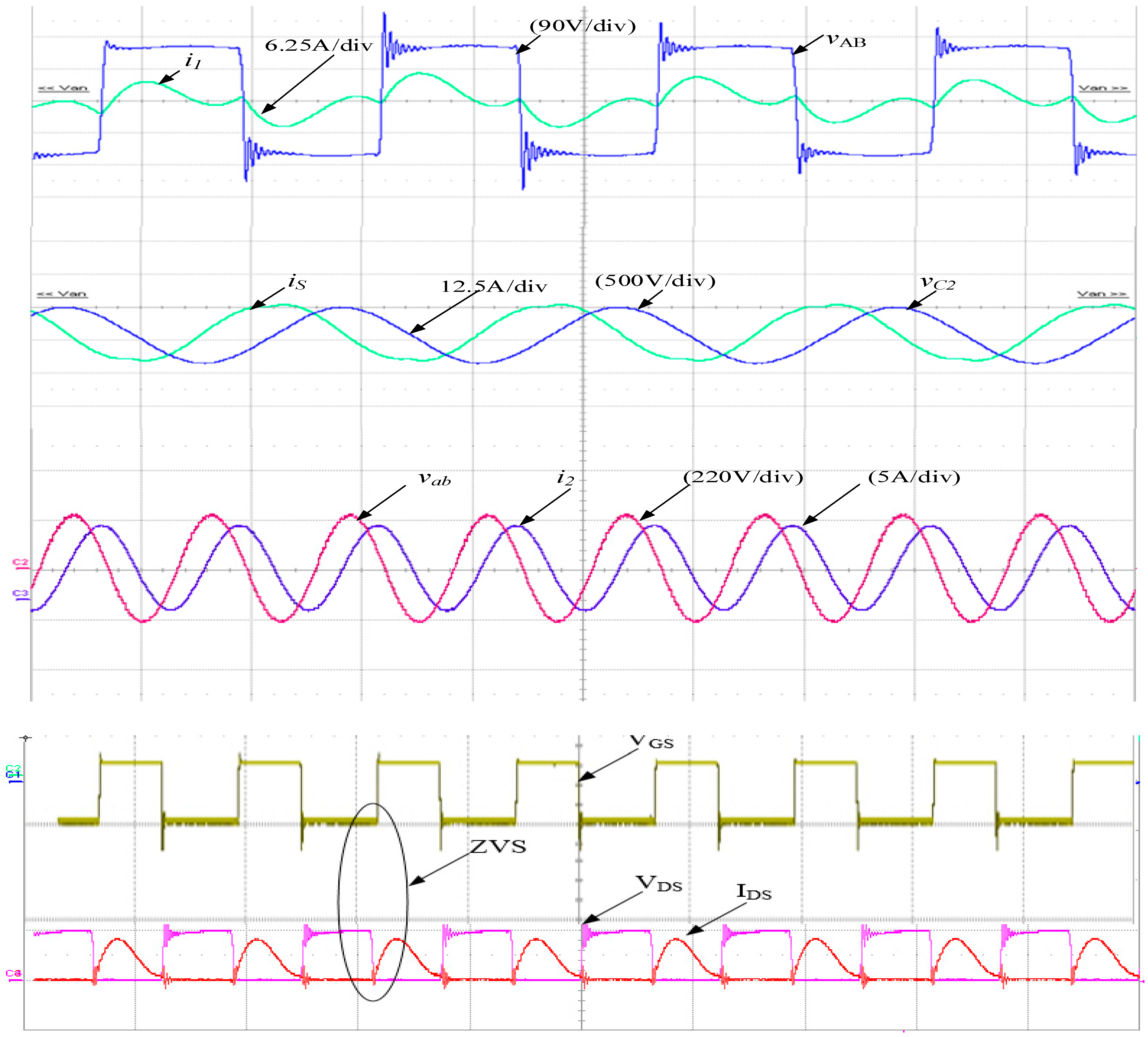
At the defined air gap, the current i1 is in phase with the high frequency inverter output voltage VAB. ZVS condition is also observed in case of experimental result which is also shown in Figure 11. In this case, VDS and IDS are the switch voltage and current of the high frequency inverter; VGS is the gate signal.
In case of higher-order harmonics injection to the rectifier side, LC-LC2 is better than the S-SP compensation technique because of the effect of equivalent inductance . Comparison between S-SP compensation and LC-LC2 compensation is shown in Table 2.
Though above comparison table is for different power rating, efficiency variation by mutual inductance changes and injection of higher order harmonics are the main parameters to evaluate the proposed network. Efficiency variation is not so much affected by the mutual inductance changes in case of proposed compensation based resonant converter in comparison to the S-SP compensation based resonant converter, shown in Figure 8 and Figure 9. Because of an additional receiving side inductor, proposed compensation technique cannot inject higher order harmonics to the rectifier side.
6. Conclusions
The proposed LC-LC2 compensated resonant converter provides the input impedance with ZPA and voltage gain having load independent characteristics at a common resonant frequency. Using a common resonant frequency, experimental results of the proposed LC-LC2 compensated resonant converter are obtained. Laboratory results represent the efficacy of the proposed compensation method with a maximum efficiency of 93%. In IPT based EV charging application, efficiency is directly related to the air gap variation. Efficiency-comparison between LC-LC2 and S-SP compensated resonant converter depicts that efficiency of the LC-LC2 compensated resonant converter is not much sensitive to the air gap variation than the S-SP compensated resonant converter. Due to the less sensitivity of the air gap variation, proposed compensation technique is very much effective in the IPT based EV charging application.
Author Contributions
Theoretical observation, simulation, experimental tests, and preparing the article are contributed by M.M.A.; S.M. has the contribution in experimental tests and preparation of the article, H.B. has the contribution in theoretical approaches and preparing the article and M.J.H.R. has contributed to the theoretical explanation and preparing the article.
Funding
The authors would like to acknowledge the financial support received from the University of Malaya, Malaysia, through Frontier Research Grant No. FG007-17AFR and Innovative Technology Grant No. RP043B-17AET.
Conflicts of Interest
There is no conflict of interest in author’s declaration.
References
- Cong, Z.; Jih-Sheng, L.; Rui, C.; Faraci, W.E.; Zahid, Z.U.; Bin, G.; Anderson, D. High-Efficiency Contactless Power Transfer System for Electric Vehicle Battery Charging Application. IEEE J. Emerg. Sel. Top. Power Electron. 2015, 3, 65–74. [Google Scholar] [CrossRef]
- Zhong, C.; Wuwei, J.; Xueliang, H.; Linlin, T.; Chen, C.; Wang, W. A Promoted Design for Primary Coil in Roadway-Powered System. IEEE Trans. Magn. 2015, 51, 1–4. [Google Scholar] [CrossRef]
- Sallan, J.; Villa, J.L.; Llombart, A.; Sanz, J.F. Optimal Design of ICPT Systems Applied to Electric Vehicle Battery Charge. IEEE Trans. Ind. Electron. 2009, 56, 2140–2149. [Google Scholar] [CrossRef]
- Lu, F.; Zhang, H.; Hofmann, H.; Mi, C. A Dynamic Charging System with Reduced Output Power Pulsation for Electric Vehicles. IEEE Trans. Ind. Electron. 2016, 63, 6580–6589. [Google Scholar] [CrossRef]
- Kainan, C.; Zhengming, Z. Analysis of the Double-Layer Printed Spiral Coil for Wireless Power Transfer. IEEE J. Emerg. Sel. Top. Power Electron. 2013, 1, 114–121. [Google Scholar]
- Raju, S.; Rongxiang, W.; Mansun, C.; Yue, C.P. Modeling of Mutual Coupling Between Planar Inductors in Wireless Power Applications. IEEE Trans. Power Electron. 2014, 29, 481–490. [Google Scholar] [CrossRef]
- Chen, Q.; Wong, S.C.; Tse, C.K.; Ruan, X. Analysis, Design, and Control of a Transcutaneous Power Regulator for Artificial Hearts. IEEE Trans. Biomed. Circuits Syst. 2009, 3, 23–31. [Google Scholar] [CrossRef] [PubMed]
- Klontz, K.W.; Divan, D.M.; Novotny, D.W.; Lorenz, R.D. Contactless power delivery system for mining applications. In Proceedings of the Conference Record of the 1991 IEEE Industry Applications Society Annual Meeting, Dearborn, MI, USA, 28 September–4 October 1991; pp. 1263–1269. [Google Scholar]
- Budhia, M.; Boys, J.T.; Covic, G.A.; Chang-Yu, H. Development of a Single-Sided Flux Magnetic Coupler for Electric Vehicle IPT Charging Systems. IEEE Trans. Ind. Electron. 2013, 60, 318–328. [Google Scholar] [CrossRef]
- Wei, Z.; Siu-Chung, W.; Tse, C.K.; Qianhong, C. Design for Efficiency Optimization and Voltage Controllability of Series-Series Compensated Inductive Power Transfer Systems. IEEE Trans. Power Electron. 2014, 29, 191–200. [Google Scholar]
- Huh, J.; Lee, S.W.; Lee, W.Y.; Cho, G.H.; Rim, C.T. Narrow-Width Inductive Power Transfer System for Online Electrical Vehicles. IEEE Trans. Power Electron. 2011, 26, 3666–3679. [Google Scholar] [CrossRef]
- Chwei-Sen, W.; Covic, G.A.; Stielau, O.H. Power transfer capability and bifurcation phenomena of loosely coupled inductive power transfer systems. IEEE Trans. Ind. Electron. 2004, 51, 148–157. [Google Scholar]
- Raabe, S.; Covic, G.A. Practical Design Considerations for Contactless Power Transfer Quadrature Pick-Ups. IEEE Trans. Ind. Electron. 2013, 60, 400–409. [Google Scholar] [CrossRef]
- Keeling, N.A.; Covic, G.A.; Boys, J.T. A Unity-Power-Factor IPT Pickup for High-Power Applications. IEEE Trans. Ind. Electron. 2010, 57, 744–751. [Google Scholar] [CrossRef]
- Wu, H.H.; Gilchrist, A.; Sealy, K.D.; Bronson, D. A High Efficiency 5 kW Inductive Charger for EVs Using Dual Side Control. IEEE Trans. Ind. Inform. 2012, 8, 585–595. [Google Scholar] [CrossRef] [Green Version]
- Wei, Z.; Siu-Chung, W.; Tse, C.K.; Qianhong, C. Analysis and Comparison of Secondary Series- and Parallel-Compensated Inductive Power Transfer Systems Operating for Optimal Efficiency and Load-Independent Voltage-Transfer Ratio. IEEE Trans. Power Electron. 2014, 29, 2979–2990. [Google Scholar]
- Villa, J.L.; Sallan, J.; Sanz, J.F.; Llombart, A. High-Misalignment Tolerant Compensation Topology For ICPT Systems. IEEE Trans. Ind. Electron. 2012, 59, 945–951. [Google Scholar] [CrossRef]
- Hou, J.; Chen, Q.; Yan, K.; Ren, X.; Wong, S.C.; Tse, C.K. Analysis and control of S/SP compensation contactless resonant converter with constant voltage gain. In Proceedings of the IEEE Energy Conversion Congress and Exposition, Denver, CO, USA, 15–19 September 2013; pp. 2552–2558. [Google Scholar]
- Budhia, M.; Covic, G.A.; Boys, J.T.; Chang-Yu, H. Development and evaluation of single sided flux couplers for contactless electric vehicle charging. In Proceedings of the IEEE Energy Conversion Congress and Exposition (ECCE), Phoenix, AZ, USA, 17–22 September 2011; pp. 614–621. [Google Scholar]
- Ahmed, K.; Aamir, M.; Uddin, M.K.; Mekhilef, S. A new coil design for enhancement in misalignment tolerance of Wireless Charging System. In Proceedings of the IEEE Student Conference on Research and Development (SCOReD), Kuala Lumpur, Malaysia, 13–14 December 2015; pp. 215–219. [Google Scholar]
- Boys, J.T.; Covic, G.A.; Green, A.W. Stability and control of inductively coupled power transfer systems. IEEE Proc.-Electr. Power Appl. 2000, 147, 37–43. [Google Scholar] [CrossRef]
- Chwei-Sen, W.; Stielau, O.H.; Covic, G.A. Design considerations for a contactless electric vehicle battery charger. IEEE Trans. Ind. Electron. 2005, 52, 1308–1314. [Google Scholar]
- Zhu, Q.; Wang, L.; Guo, Y.; Liao, C.; Li, F. Applying LCC Compensation Network to Dynamic Wireless EV Charging System. IEEE Trans. Ind. Electron. 2016, 63, 6557–6567. [Google Scholar] [CrossRef]
- Weihan, L.; Han, Z.; Tianze, K.; Mi, C. Inter-operability considerations of the double-sided LCC compensated wireless charger for electric vehicle and plug-in hybrid electric vehicle applications. In Proceedings of the IEEE PELS Workshop on Emerging Technologies: Wireless Power (2015 WoW), Daejeon, Korea, 5–6 June 2015; pp. 1–6. [Google Scholar]
- Xiaoyong, R.; Qianhong, C.; Lingling, C.; Xinbo, R.; Siu-Chung, W.; Tse, C.K. Characterization and control of self-oscillating contactless resonant converter with fixed voltage gain. In Proceedings of the 7th International Power Electronics and Motion Control Conference, Harbin, China, 2–5 June 2012; pp. 1822–1827. [Google Scholar]
- Hasanzadeh, S.; Vaez-Zadeh, S. Enhancement of overall coupling coefficient and efficiency of contactless energy transmission systems. In Proceedings of the 2nd Power Electronics, Drive Systems and Technologies Conference, Tehran, Iran, 16–17 February 2011; pp. 638–643. [Google Scholar]
- Li, W.; Zhao, H.; Li, S.; Deng, J.; Kan, T.; Mi, C.C. Integrated LCC Compensation Topology for Wireless Charger in Electric and Plug-in Electric Vehicles. IEEE Trans. Ind. Electron. 2015, 62, 4215–4225. [Google Scholar] [CrossRef]
- Huang, C.Y.; Boys, J.T.; Covic, G.A. LCL Pickup Circulating Current Controller for Inductive Power Transfer Systems. IEEE Trans. Power Electron. 2013, 28, 2081–2093. [Google Scholar] [CrossRef]
- Amjad, M.; Salam, Z.; Facta, M.; Mekhilef, S. Analysis and Implementation of Transformerless LCL Resonant Power Supply for Ozone Generation. IEEE Trans. Power Electron. 2013, 28, 650–660. [Google Scholar] [CrossRef] [Green Version]
Figure 1.
Equivalent circuit of the LC-LC2 compensation network.
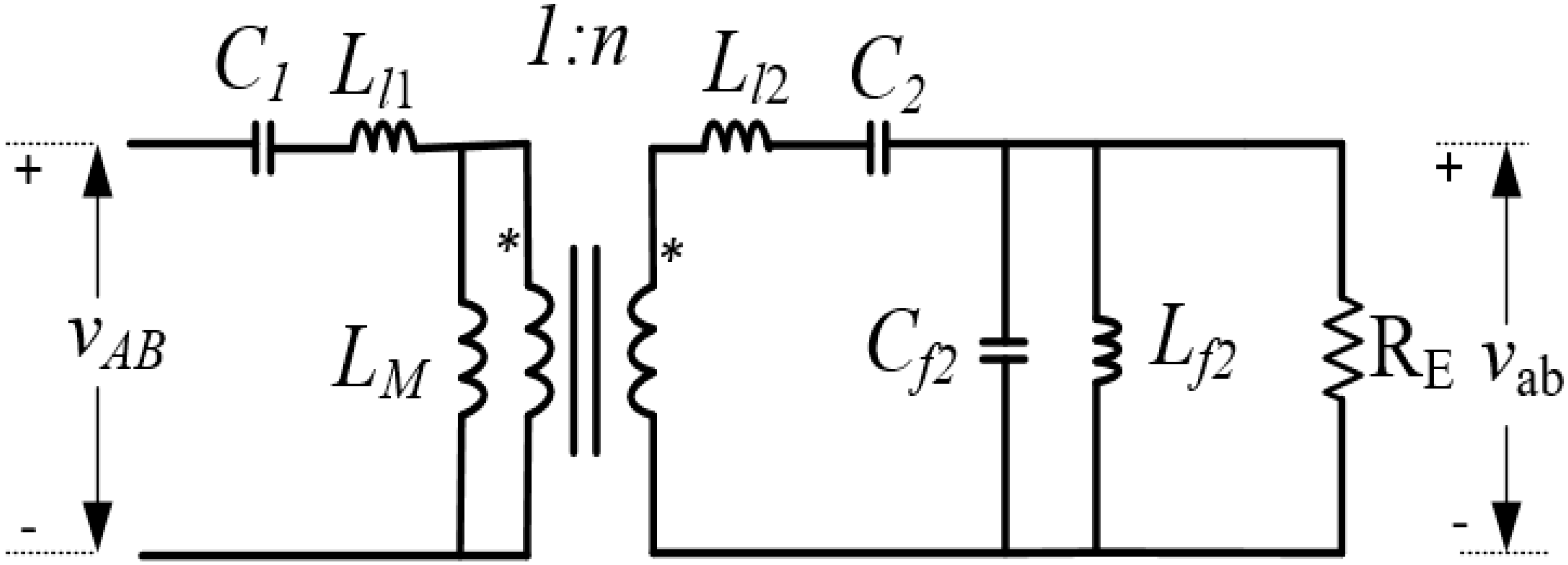
Figure 2.
Proposed LC-LC2 compensated resonant converter.

Figure 3.
Equivalent circuit for switching mode (a) Mode 1 [t0–t1]; (b) Mode 2 [t1–t2]; (c) Mode 3 [t2–t3]; (d) Mode 4 [t3–t4].
Figure 3.
Equivalent circuit for switching mode (a) Mode 1 [t0–t1]; (b) Mode 2 [t1–t2]; (c) Mode 3 [t2–t3]; (d) Mode 4 [t3–t4].

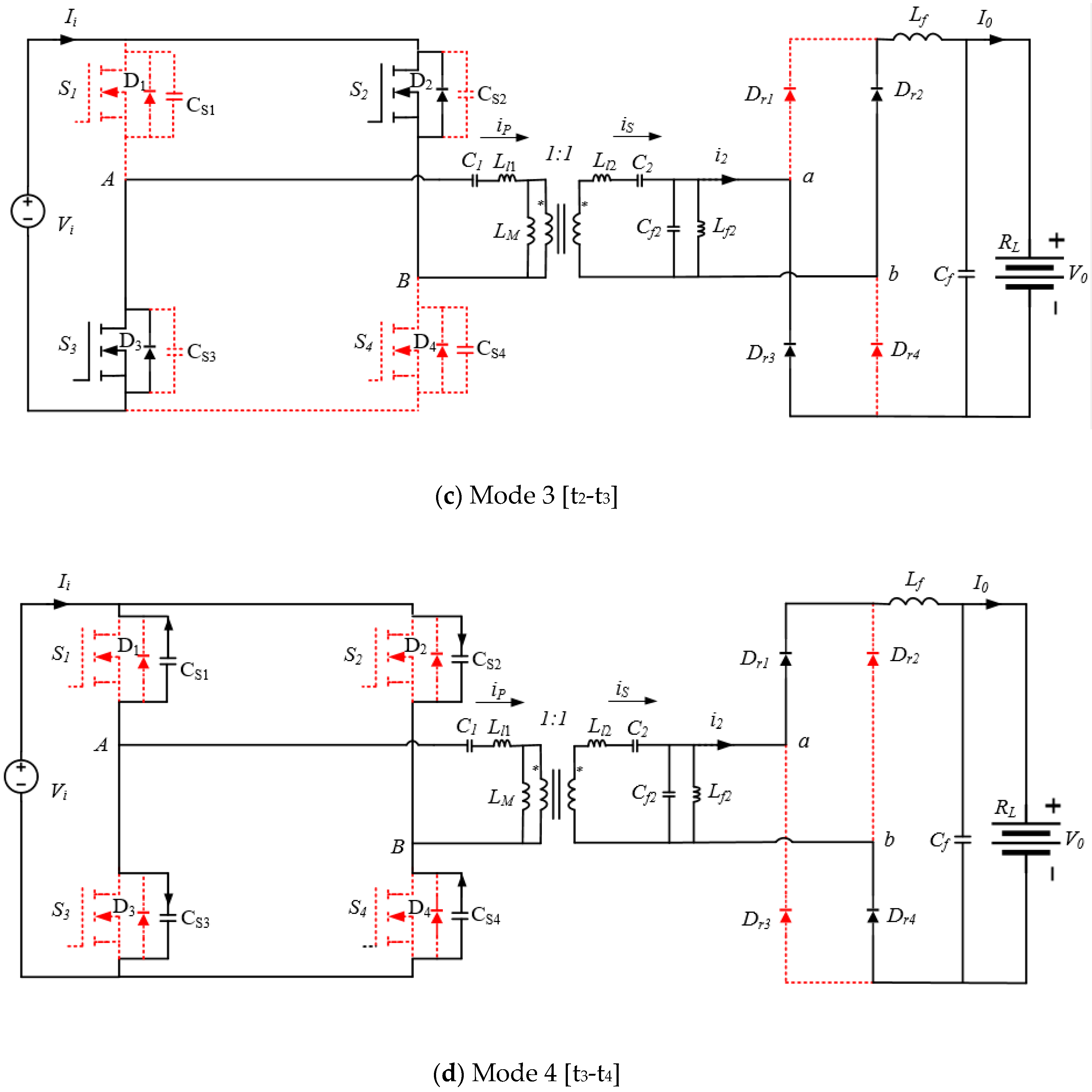
Figure 4.
Operating waveforms of the proposed LC-LC2 resonant converter.

Figure 5.
Measured input phase angle of the 500 W LC-LC2 compensated resonant converter.

Figure 6.
Measured voltage gain of the 500 W LC-LC2 compensated resonant converter.
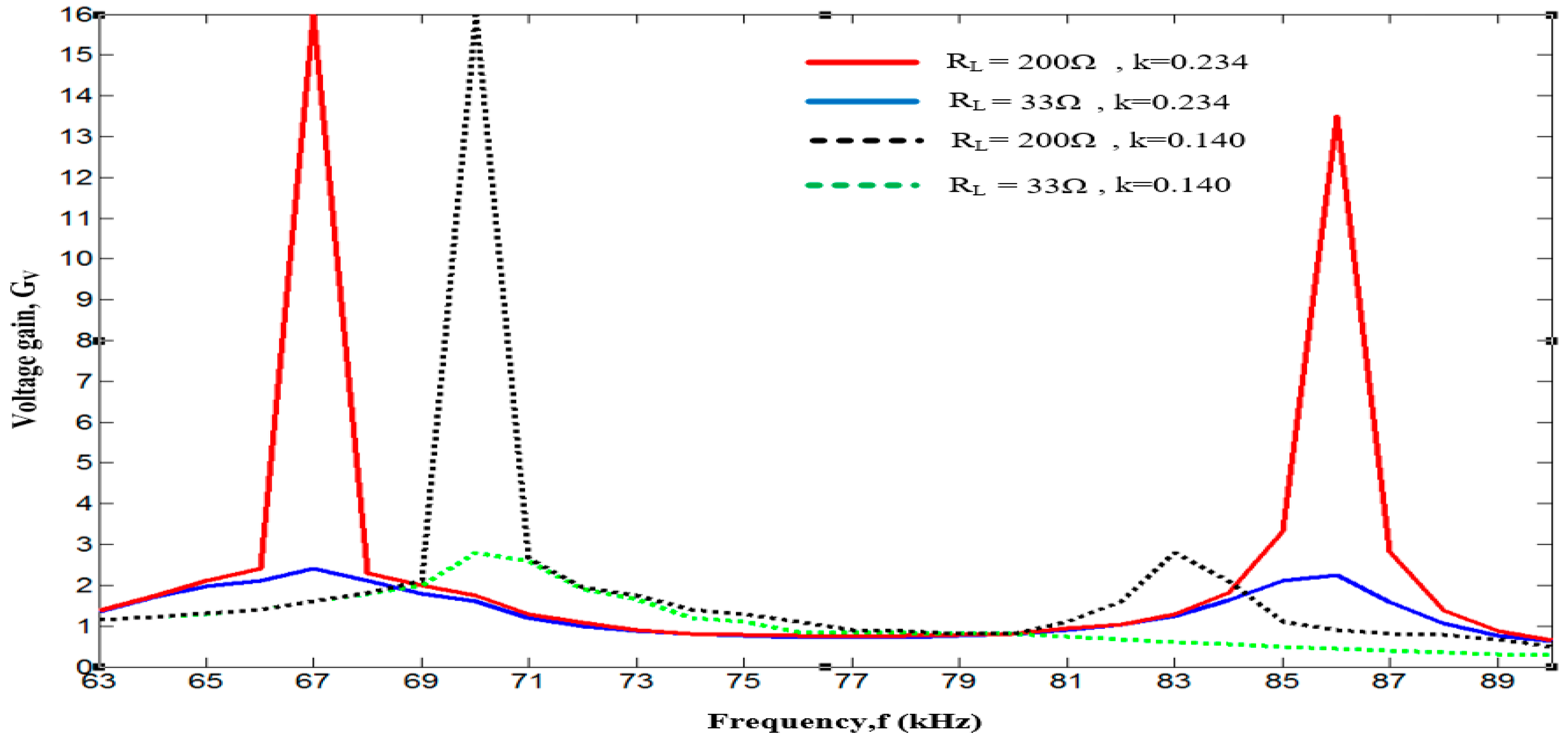
Figure 7.
Measured load regulation of the 500 W LC-LC2 compensated resonant converter.

Figure 8.
The efficiency of the 500 W LC-LC2 compensated resonant converter.

Figure 9.
The efficiency of the 500 W S–SP compensated resonant converter.

Figure 10.
Laboratory results of the proposed LC-LC2 compensated resonant converter.
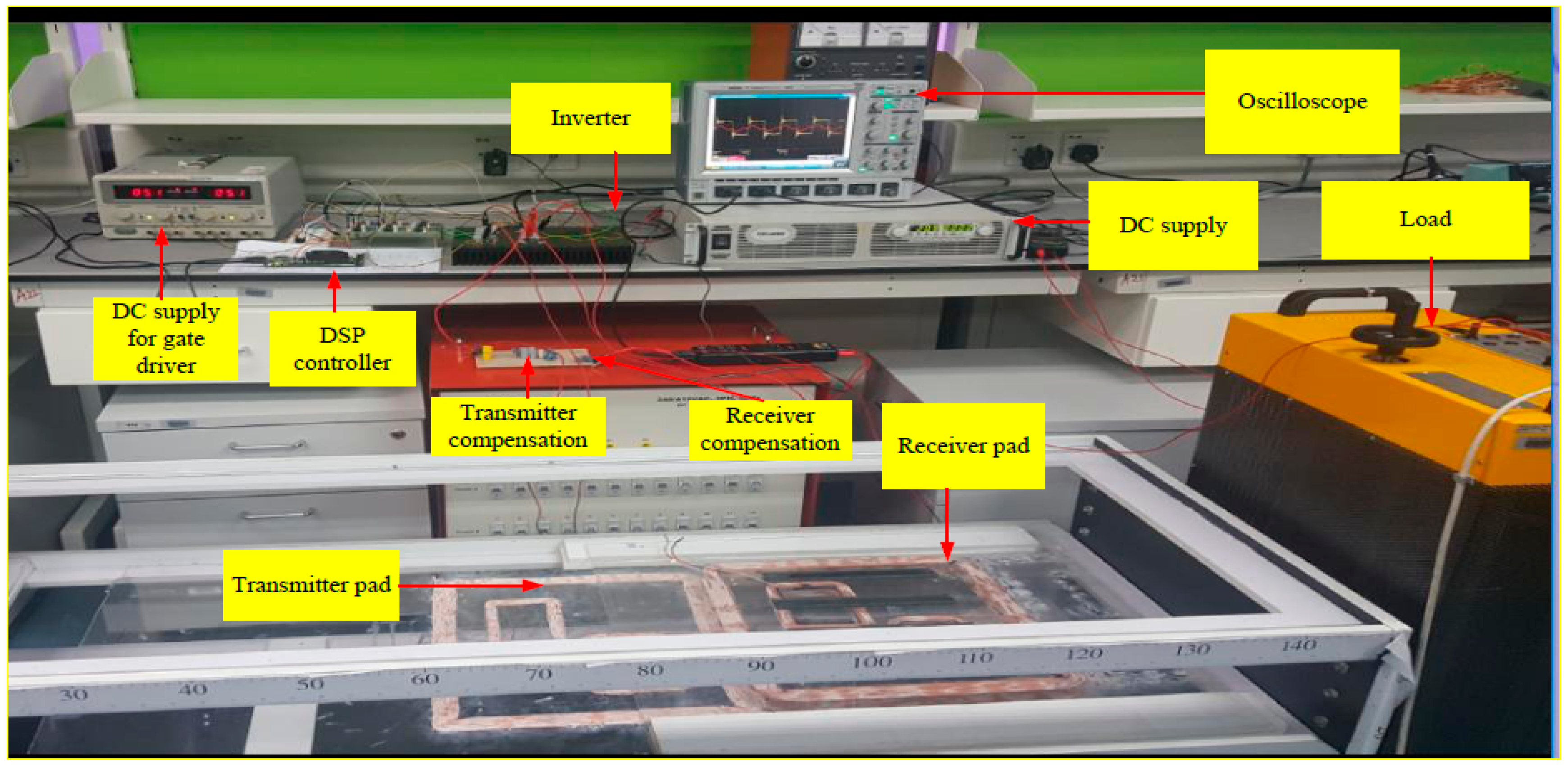
Figure 11.
Laboratory results of the proposed LC-LC2 compensated resonant converter.

Table 1.
Design specifications of the LC-LC2 converter.
| Design Specifications | Value |
|---|---|
| Resonant frequency | f = 80 kHz |
| Parameters of IPT transformer | n = 1, Ll1 = 82.95 µH, Ll2 = 82.05 µH, LM = 25.25 µH–13.1 µH, k = 0.234–0.140 |
| Compensating inductor | Lf2 = 20 µH |
| Resonant capacitors | C1 = 47.71 nF, C2 = 48.24 nF, Cf2 = 354.65 nF |
| Load resistance | RL = 33–200 Ω |
| Filter parameters | Lf = 1000 µH and Cf = 500 nF |
| Load power | PL = 500 W |
| Air gap | H = 140–180 mm |
Table 2.
Comparison of LC-LC2 compensation with S–SP2 compensation.
| Compensation Networks | Evaluation Criteria | ||||
|---|---|---|---|---|---|
| Maximum Efficiency | Power Rating | Air Gap | Efficiency Variation | Higher-Order Harmonics | |
| S–SP [18] | 93% | 1500 W | 200 mm | Affected by the mutual inductance changes | Injected to the rectifier side |
| LC-LC2 | 93% | 500 W | 140 mm | Less affected by the mutual inductance changes | Not injected to the rectifier side |
© 2018 by the authors. Licensee MDPI, Basel, Switzerland. This article is an open access article distributed under the terms and conditions of the Creative Commons Attribution (CC BY) license (http://creativecommons.org/licenses/by/4.0/).
Share and Cite
MDPI and ACS Style
Alam, M.M.; Mekhilef, S.; Bassi, H.; Rawa, M.J.H. Analysis of LC-LC2 Compensated Inductive Power Transfer for High Efficiency and Load Independent Voltage Gain. Energies 2018, 11, 2883. https://doi.org/10.3390/en11112883
AMA Style
Alam MM, Mekhilef S, Bassi H, Rawa MJH. Analysis of LC-LC2 Compensated Inductive Power Transfer for High Efficiency and Load Independent Voltage Gain. Energies. 2018; 11(11):2883. https://doi.org/10.3390/en11112883
Chicago/Turabian StyleAlam, Md Morshed, Saad Mekhilef, Hussain Bassi, and Muhyaddin Jamal Hosin Rawa. 2018. "Analysis of LC-LC2 Compensated Inductive Power Transfer for High Efficiency and Load Independent Voltage Gain" Energies 11, no. 11: 2883. https://doi.org/10.3390/en11112883
Note that from the first issue of 2016, this journal uses article numbers instead of page numbers. See further details here.