A Quasi-Resonant ZVZCS Phase-Shifted Full-Bridge Converter with an Active Clamp in the Secondary Side


Electrical Engineering Department, Soongsil University, 369 Sang-doro, Seoul, Korea
*
Author to whom correspondence should be addressed.
Energies 2018, 11(11), 2868; https://doi.org/10.3390/en11112868
Submission received: 11 October 2018
/
Revised: 19 October 2018
/
Accepted: 22 October 2018
/
Published: 23 October 2018
Abstract
:A novel Pulse-Width-Modulation (PWM) quasi-resonant active-clamp phase-shifted full-bridge converter is presented and analyzed in this paper. In the proposed topology, an active-clamp switch and a clamp capacitor that resonates with the leakage inductance of transformer are employed at the secondary side. The active-clamp circuit helps all of the primary switches in achieving both zero-voltage switching (ZVS) turn-on and nearly zero-current switching (ZCS) turn-off over the entire load range, and resets the primary current during the freewheeling interval. The operation of the active-clamp circuit eliminates voltage ringing across the rectifier. In addition, the secondary diodes can achieve ZCS turn-off, which removes the reverse recovery problem of diodes, and the active-clamp switch can achieve ZCS turn-on. A 3.5-kW prototype was built to verify the performance of the proposed converter. A maximum efficiency of 97.6% was achieved under a 2-kW load, and an efficiency of more than 96% was achieved even under a light load.
1. Introduction
The on-board chargers of electric vehicles (EVs) typically consist of an alternating current/direct current (AC–DC) converter and a DC–DC converter. The AC–DC converter transforms commercial AC into DC with a power factor correction function, and the DC–DC converter charges batteries via a certain charge method, such as constant-current/constant-voltage charging [1,2,3]. Efficiency and compactness are the most important factors in optimization during charger design because fuel efficiency is one of the most crucial factors that characterizes EV performance. For the DC–DC converters of on-board chargers, a traditional phase-shifted full-bridge (PSFB) converter is often adopted because the zero-voltage turn-on for all of the primary switches is possible. However, PSFB converters have several drawbacks [4,5,6,7] such as a narrow zero-voltage switching (ZVS) range for the lagging leg switches, a circulating current that increases conduction loss, duty cycle loss, voltage oscillations, and a reverse recovery current of the rectifier diodes.
The literature reports two main technical solutions to the disadvantages of PSFB converters. One solution is to extend the ZVS range for lagging leg switches by creating an auxiliary-current source, (as shown in Figure 1a), which preserves sufficient inductive energy to discharge the output capacitors of the switches during transition. The auxiliary-current source can be realized through the large leakage inductance of the transformer or an external inductor connected in series with the transformer [8]. However, a large inductance at the primary side leads to a large duty cycle loss. In this case, the turns ratio of the transformer needs to increase to obtain the required output voltage. However, this results in an elevated voltage stress of the output rectifier diodes. The auxiliary-current source, , can be realized via the other methods such as current-enhancement techniques [9,10] or a hybrid PWM technique with a shared lagging leg [11]. However, these auxiliary-current source networks can be implemented in exchange for increases in the volume, cost, and power loss of a converter.
The other solution is to reset the circulating current and to dampen the voltage ringing by creating a blocking-voltage source, (as shown in Figure 1b), which creates a higher voltage than the input source. The blocking-voltage source can be created by placing a large blocking capacitor at the primary side [12] or by using a passive clamp circuit [12,13,14,15,16,17] or an active-clamp circuit [18,19,20,21] at the secondary side. Normally, a secondary clamp circuit is preferred because it does not require a large capacitor that increases the volume and cost. In References [22,23,24,25], a blocking-voltage source was created at the secondary side of the voltage-doubler topology [22,23,24,25]. This technique utilizes the resonance between the leakage inductor of the transformer and the secondary rectifier capacitor to deliver energy. However, it has some disadvantages, such as the relatively large current rating of the rectifier diodes, the incomplete elimination of the circulating current, and the dependence of the zero-current switching (ZCS) condition for the primary switches on the load current. The common idea behind both passive and active circuits is to utilize the resonance between the clamp capacitor and the leakage inductor of the transformer. Since the clamp capacitor has a higher voltage than the primary side of the transformer due to resonance, the energy transfer from the primary side to the secondary side is blocked during the freewheeling interval. While the resonance between the leakage inductor of the transformer and the clamp capacitor cannot be controlled in passive clamp techniques, it can be controlled in active-clamp techniques by the active switch. Normally, the active-clamp switch is controlled two times in a switching cycle, and the discharge of the clamp capacitor and the decay of the primary current are triggered by the turn-on of the active-clamp switch.
A performance comparison of PSFB converters with several kinds of passive and active-clamp circuits is shown in Table 1.
There are two kinds of variations in terms of active-clamp topologies, as shown in Figure 2. The active-clamp circuit was connected across the output filter inductor in Reference [26] (Figure 2a), while it was connected across the rectifier bridge in References [18,27,28] (Figure 2b). However, the topology in Figure 2a requires an additional diode for freewheeling when it is applied to topologies with a center-tapped transformer. In other studies, these active-clamp circuits were further modified by adding an auxiliary transformer [20], a diode [19], or even a buck converter [21]. However, these topologies are expensive and complex due to the additional components, which leads to lower efficiency of the converters.
One of the significant contributions of the proposed active-clamp control method when compared to previous methods is the ZCS turn-off of the leading-leg switches, as shown in Table 2. It can be noted from the switching schemes shown in References [18,26] that the active-clamp switch is turned on after the leading-leg switch is turned-off. In conventional PSFB converters, since the primary current is equal to the reflected load current when the leading leg switch is turned off, it is not possible to achieve ZCS turn-off for the leading-leg switches. In Reference [27], the active-clamp switch is turned on before the leading-leg switch is turned off. However, since the resonance frequency of and is significantly lower than the switching frequency, the maximum voltage across the clamp capacitor is equal to the reflected input voltage during a switching period. Therefore, the primary current increases continuously until the switch is turned off, which leads to hard-switching turn-off of the switch , which is the same as conventional PSFB converters.
In order to achieve ZCS turn-off for the leading-leg switches in active-clamp PSFB converters, a novel method is proposed to realize the blocking-voltage source across the secondary rectifier bridge before the active switch is turned on. In the proposed method, the resonance frequency of and is selected to be even higher than the switching frequency. When the active-clamp switch is turned on, starts resonating with , and the voltage across the secondary rectifier bridge is increased higher than the reflected input voltage . Thanks to this blocking-voltage source, the primary current decreases quickly to be equal to the magnetizing current before the leading-leg switch is turned off. It is necessary to minimize the magnetizing current to archive a nearly ZCS turn-off condition for the leading switch , while the ZVS turn-on condition is maintained.
ZCS turn-off is especially important for converters employing insulated-gate bipolar transistors (IGBTs) since they suffer from the tail-current problem [18]. The minority carrier in an IGBT can be swept out before turning off if the ZCS turn-off of the IGBT switch is achieved. Then, it is possible to increase the switching frequency of the converter without lowering efficiency, which makes it attractive for the wide-load-range and high-power applications where IGBTs are predominantly used as power switches.
In this paper, a new control scheme for active-clamp PSFB converters is proposed (as shown in Figure 2b), including the design of the clamp capacitor to achieve ZCS turn-off for the leading-leg switches, while maintaining all of the advantages of conventional active-clamp techniques. It should be noted that, although the topologies in References [18,27] and the proposed converter are the same, the operating principles, and hence, the performances of the converters are totally different. In the proposed converter, the leakage inductance of the transformer resonates with the clamp capacitor. The converter operates at a fixed resonant frequency and the output voltage is regulated by phase shift control, while the active switch is controlled to achieve the ZCS turn-off condition for the primary switches. The outstanding characteristics of the proposed converter are as follows:
- ▪
- ZVS turn-on for all of the primary switches over the entire load range.
- ▪
- Nearly ZCS turn-off for all of the primary switches over the entire load range.
- ▪
- Complete elimination of the circulating current during freewheeling, which eliminates its associated losses.
- ▪
- No reverse recovery for the secondary rectifier diodes.
- ▪
- Little duty cycle loss.
- ▪
- Elimination of the voltage ringing at the secondary circuit.
- ▪
- High efficiency over the entire load range.
This paper consists of five sections. The introduction is given in Section 1. The operational principle of the proposed zero-voltage zero-current switching (ZVZCS) converter is analyzed in Section 2, and an analysis of the proposed converter is presented in Section 3. To validate the proposed converter, a 3.5-kW prototype was built and the experimental results are shown in Section 4. Finally, some conclusions are given in Section 5.
2. Operational Principle of the Proposed Quasi-Resonant ZVZCS PSFB Converter
The circuit configuration of the proposed converter is exactly the same as that presented in Reference [18]. The proposed converter, shown in Figure 2b, differs from the conventional active-clamp PSFB converter [18] in terms of the leakage inductance of the transformer, , and the clamp capacitor, , constituting a resonant tank, which makes the primary current a quasi-sinusoidal waveform. The function of the auxiliary switch, , is to hold off the resonance between and for a period of time. is turned on to reset the primary current during freewheeling, which creates a ZCS turn-off condition for the primary switches. The output voltage is regulated by the phase-shifted control scheme of the primary-side switches.
To simplify the analysis, the output filter inductance is presumed to be large enough for consideration as an ideal current source, . Some circuit parameters are defined as follows:
- ▪
- Characteristic impedance
- ▪
- Resonant angular frequency
- ▪
- Resonant frequency
- ▪
- Switching period Ts and switching frequency fs
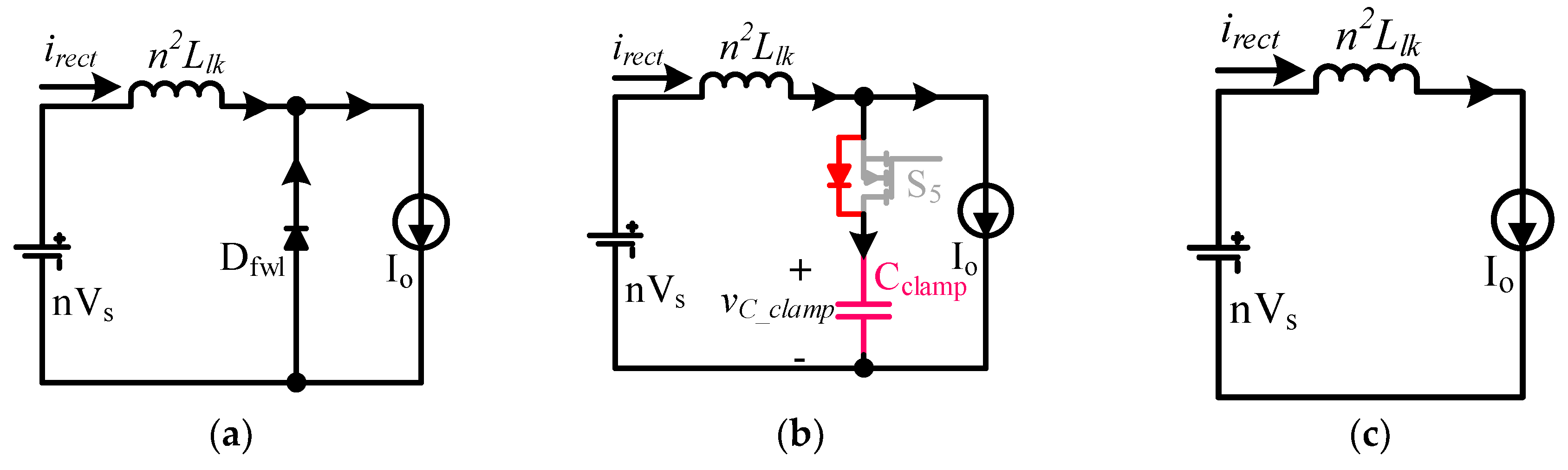
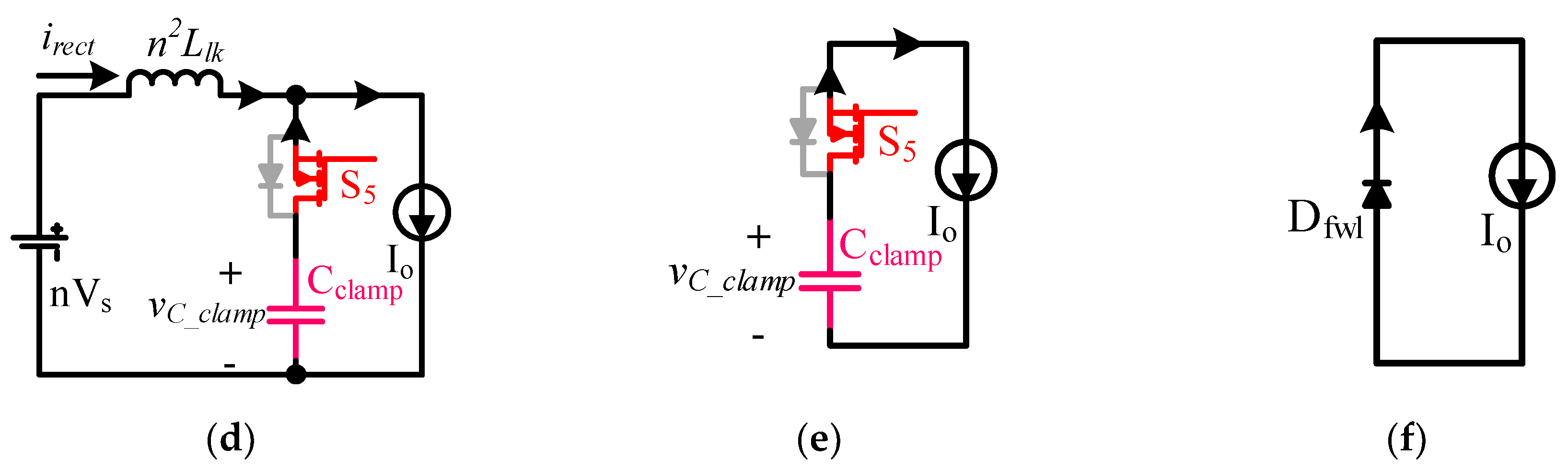
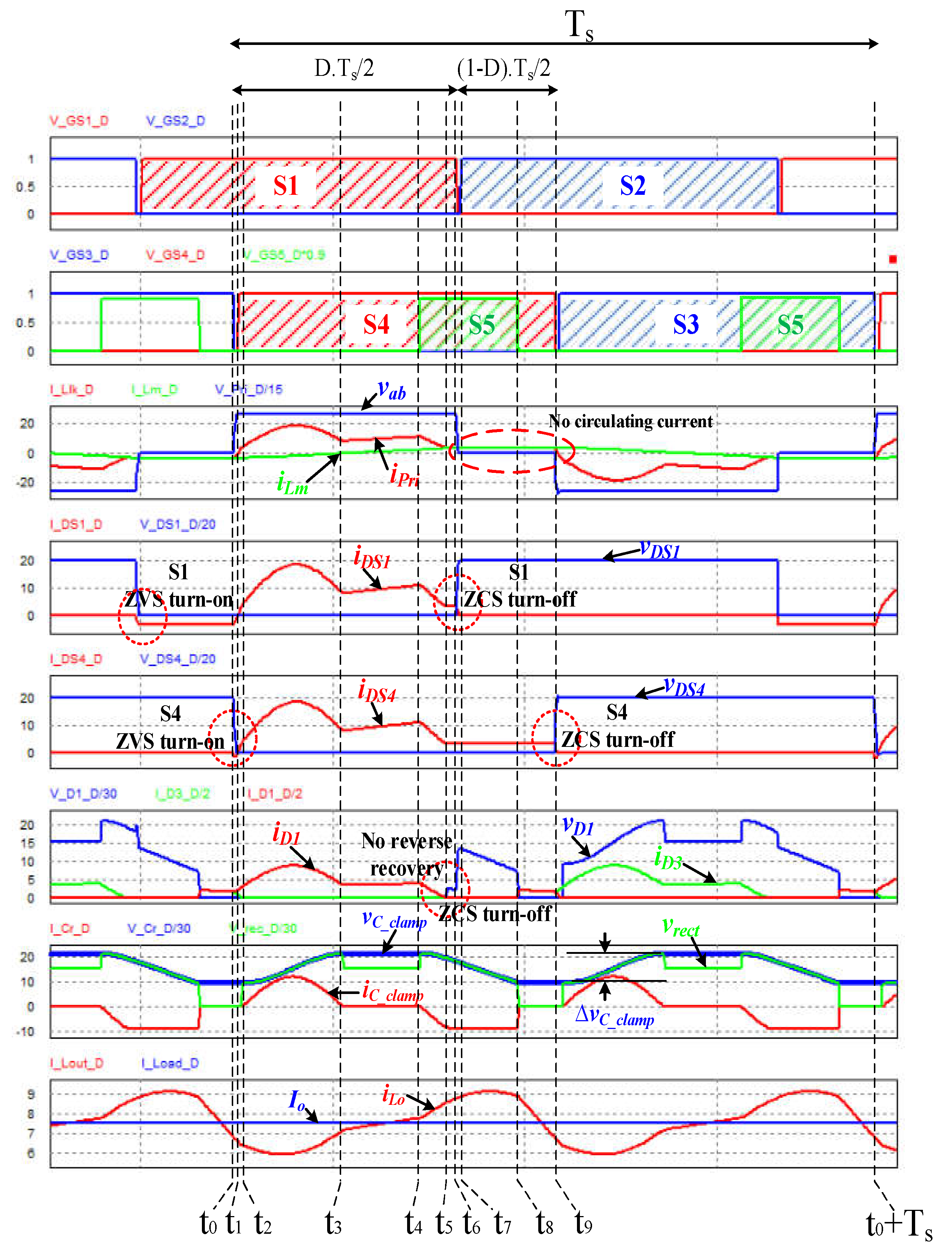
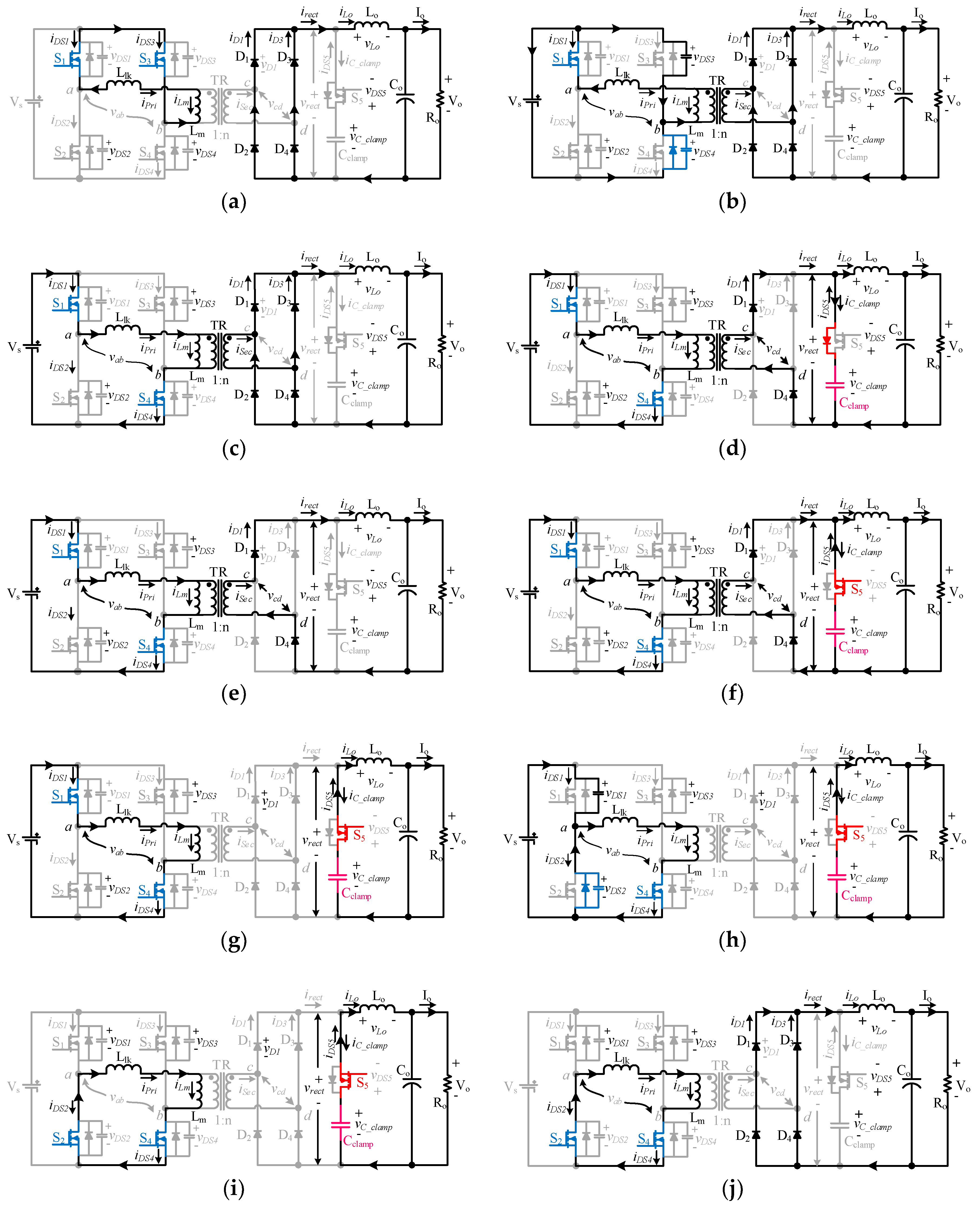
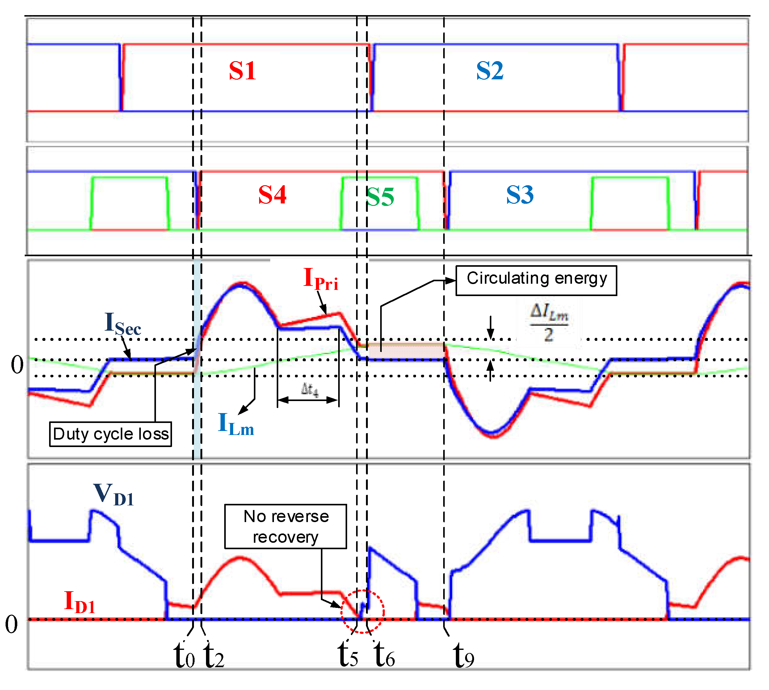
Figure 3 illustrates the key working waveforms, and Figure 4 shows the equivalent circuits of the proposed converter. The operation modes can be divided into nine modes in half of a switching period. The operating principles are explained below.
(see Figure 4a): In this mode, the magnetizing current, , circulates through the switches, and , and all of secondary rectifier diodes participate in constituting a freewheeling path for the output inductor current, .
(see Figure 4b): The switch, , turns off at and the magnetizing current, , starts charging the output capacitance of and discharging that of . After the output capacitance of is fully discharged, the voltage across drops to zero, and the body diode of the latter switch becomes forward biased and achieves the ZVS turn-on condition. To attain the ZVS operation of the lagging-leg switch, , the energy stored in the magnetizing inductance, , needs to satisfy Equation (6).
The minimum dead time, , required to guarantee the ZVS operation of the lagging-leg switches can be calculated using Equation (7).
(see Figure 4c): At , the switch, , is turned on with ZVS. The input voltage, , is applied to the leakage inductance of the transformer, . The primary current, , increases monotonically according to the slope in Equation (8).
Because does not reach the reflected output inductor current, , a power transfer does not occur from the primary side to the load. Meanwhile, linearly increases as a function of time according to Equation (9).
This mode ends when reaches the reflected output current, . The time interval in this mode, , can be calculated from Equation (10).
(see Figure 4d): At , reaches , and the diodes and become forward biased. starts resonating with . is the sum of the resonant current, and the PWM current, , reflected to the primary side and can be expressed as Equation (11).
This mode ends at when the current decreases to zero. The clamp capacitor is charged at its peak voltage at , where .
The operating interval in this mode, , can be calculated in the form of Equation (13).
(see Figure 4e): Because half of the resonance is completed at , the primary current is the same as the reflected secondary inductor current. is charged to its peak voltage and maintained at its value during this mode. The voltage across the rectifier, , is clamped to the value in Equation (14).
This mode ends when the active-clamp switch, , is turned on.
(see Figure 4f): This mode begins with the ZCS turn-on of . starts resonating with the leakage inductor. Since is reset, the secondary current, decays to zero, and is expressed as Equation (15).
Because at , Equation (15) can be written as Equation (16).
Therefore, the time interval in this mode, , can be calculated using Equation (17).
As deduced from Equation (16), Equation (18) should be satisfied to guarantee the ZCS turn-off of the primary switches and rectifier diodes.
(see Figure 4g): Although the primary switches, and , are still turned on in this mode, only a small magnetizing current flows in the primary side since the rectifier diodes become reverse-biased by . Hence, the ZCS turn-off condition for can be achieved at . At the secondary side, the energy stored in the clamp capacitor is continuously discharged to the load.
(see Figure 4h): Because is turned off at , the magnetizing current flowing in the primary side charges and discharges the output capacitor of the primary switches, and , respectively. Then, the body diode of conducts and gets ready for ZVS turn-on.
The minimum dead time, , required for guaranteeing the ZVS operation of the leading-leg switches can be calculated using Equation (19). Actually, the time interval of this mode is the same as that of Mode 1 in Equation (7).
(see Figure 4i): is turned on with ZVS at . Because the secondary switch, , is still on, the discharge current of is equal to . This mode ends when is turned off at . The time interval of this mode can be calculated through Equation (20).
(see Figure 4j): After is turned off at , the output inductor current flows through all of the rectifier diodes. Thus, is zero. Only flows through the primary side of the transformer. In this mode, the secondary side of the converter operates in a similar manner to that in . Because the other half of the operation is symmetric to the operation modes explained above, it is omitted here.
3. Analysis of the Proposed Converter
3.1. Voltage Conversion Ratio
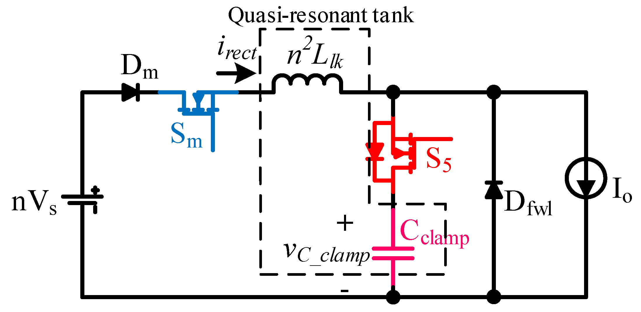
The voltage conversion ratio, (), can be derived from a simplified equivalent circuit model obtained by equating the energy, , supplied by the input source and the energy, , absorbed by the load, as shown in Figure 5. In the proposed converter, the energy is only transferred to the load during the effective duty cycle time ( between and , as shown in Figure 4. This operation can be simply represented by a switch, , operating with a duty cycle D at twice the switching frequency, . In the equivalent circuit model, the input voltage source and the leakage inductance of the transformer are reflected to the secondary side. While the rectifying function of the rectifier diodes is represented by the diode, , to keep the current from flowing in the forward direction only, the freewheeling function of the rectifier diodes in is represented by .
By equating to during a single switching cycle, the DC-voltage gain, , can be obtained as Equation (21). The detailed derivation procedure for the voltage gain of the proposed converter can be found in Appendix A.
where , , and .
As shown in Equation (21), the proposed converter possesses both resonant converter and PWM converter characteristics since the voltage gain depends on , the switching frequency, , and the effective duty cycle .
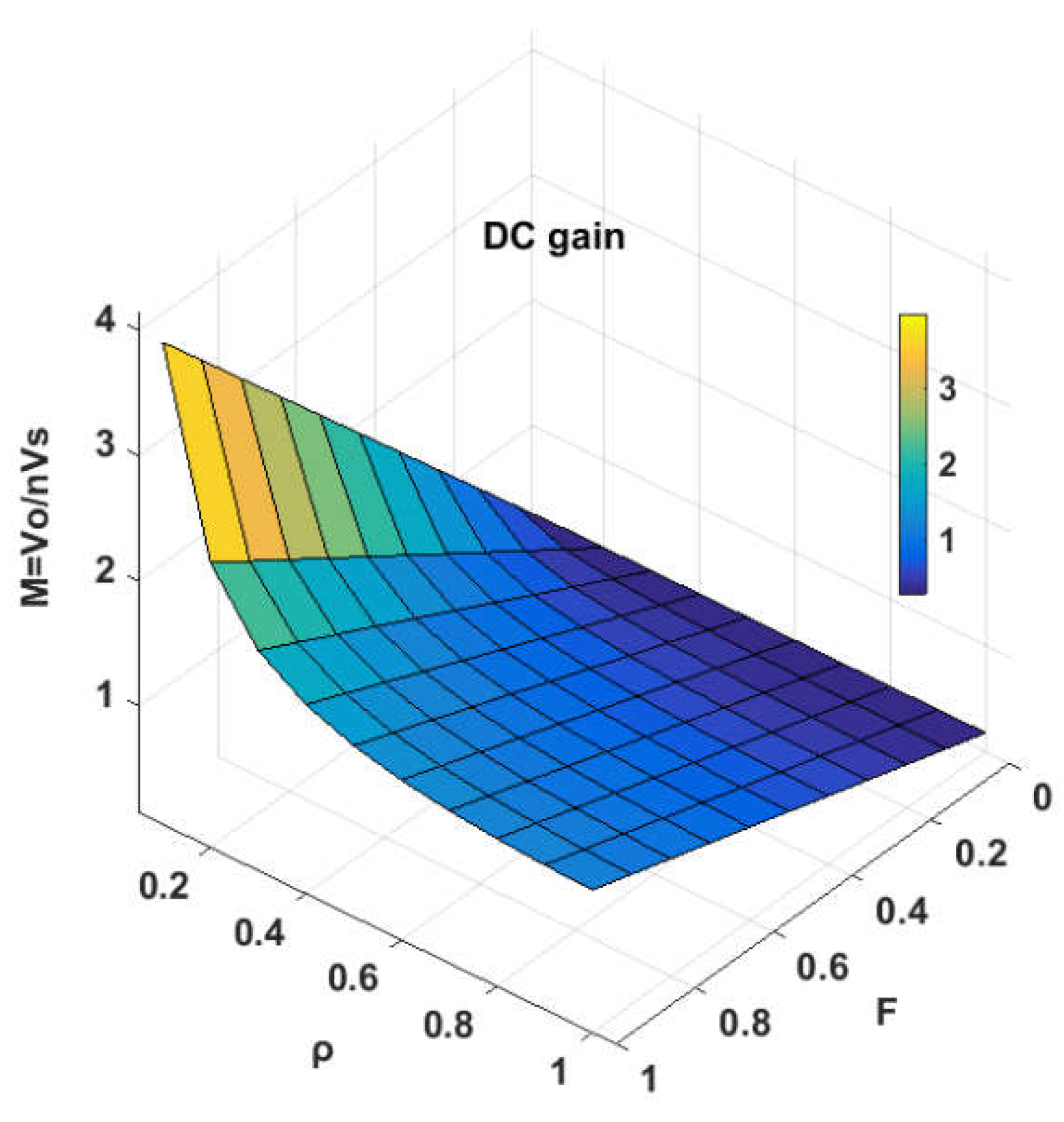
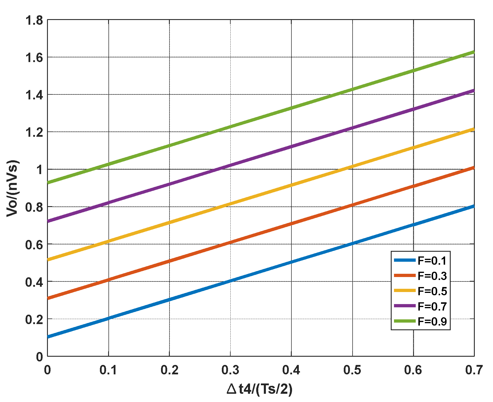
Because is the condition required to obtain ZCS turn-off of the leading-leg switches, the M value of the proposed converter can be drawn as shown in Figure 6, where the duty cycle, , is constant at 0.3. Figure 6 shows that the M value of the proposed converter does not change sharply when . Therefore, this region is preferred for the practical design of the converter.
The magnitude of M in the proposed converter is also proportional to F. Therefore, the voltage gain increases when the switching frequency increases, as shown in Figure 7, which shows that the characteristics of the proposed converter are the same as those of a resonant converter. If the switching frequency, , is fixed, the voltage gain is proportional to the effective duty cycle, as illustrated in Figure 7, which shows that the characteristics of the proposed converter are the same as those of a PWM converter.
3.2. ZVS Turn-On for All Primary Switches Regardless of the Load
In the proposed converter, the primary current in and is equal to before or is turned on, as shown in Figure 8. If the energy stored in is sufficient for discharging the of the switch and the parasitic capacitor of the transformer, the converter can create ZVS turn-on conditions for both and , regardless of the load. Therefore, Equation (22) should be satisfied to achieve ZVS turn-on conditions for all primary switches.
where is the peak-to-peak value of , and is the output capacitance of the metal-oxide-semiconductor field-effect transistor (MOSFET) switches. Hence, can be calculated from Equation (22) in the form of Equation (23).
where is the minimum effective duty when the output voltage is at its minimum.
4. Experimental Results
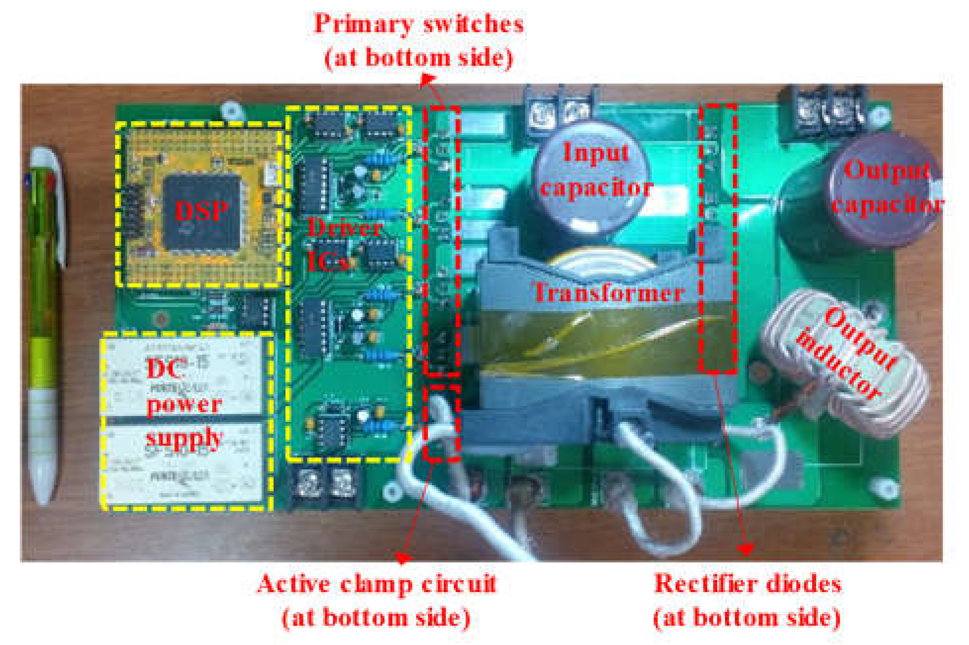
To validate the features of the proposed converter, a prototype converter (as shown in Figure 9) was designed using the specifications shown in Table 3. Table 4 and Table 5 show the design parameters and information on the components used in the prototype circuit, respectively.
Figure 10 shows experimental waveforms of the proposed converter when the output power is 3 kW. In Figure 10a,b, both the leading-leg and lagging-leg switches can achieve ZVS turn-on and ZCS turn-off. Figure 10c shows voltage and current waveforms of the primary and secondary sides of the transformer, respectively. During freewheeling, only a small magnetizing current flows through the primary side of the transformer. Therefore, the conduction loss due to the circulating current can be minimized.
Figure 10d illustrates voltage and current waveforms of the rectifier diode, . The voltage ringing of the rectifier successfully clamps to 580 V with a 400-V input. In addition, the reverse-recovery problem of the rectifier diodes does not exist in the proposed converter since the diode current, , smoothly decreases before the diode, , becomes reverse-biased.
Figure 11a shows waveform of the active clamp switch, S5. The ZCS turn-on operation of S5 can be achieved due to the resonance between Llk and Cclamp. Figure 11b shows voltage and current waveforms of the clamp capacitor. increases to a peak value of 580 V when decays to zero. starts decreasing when the switch, , turns on due to the discharge current of the clamping capacitor.
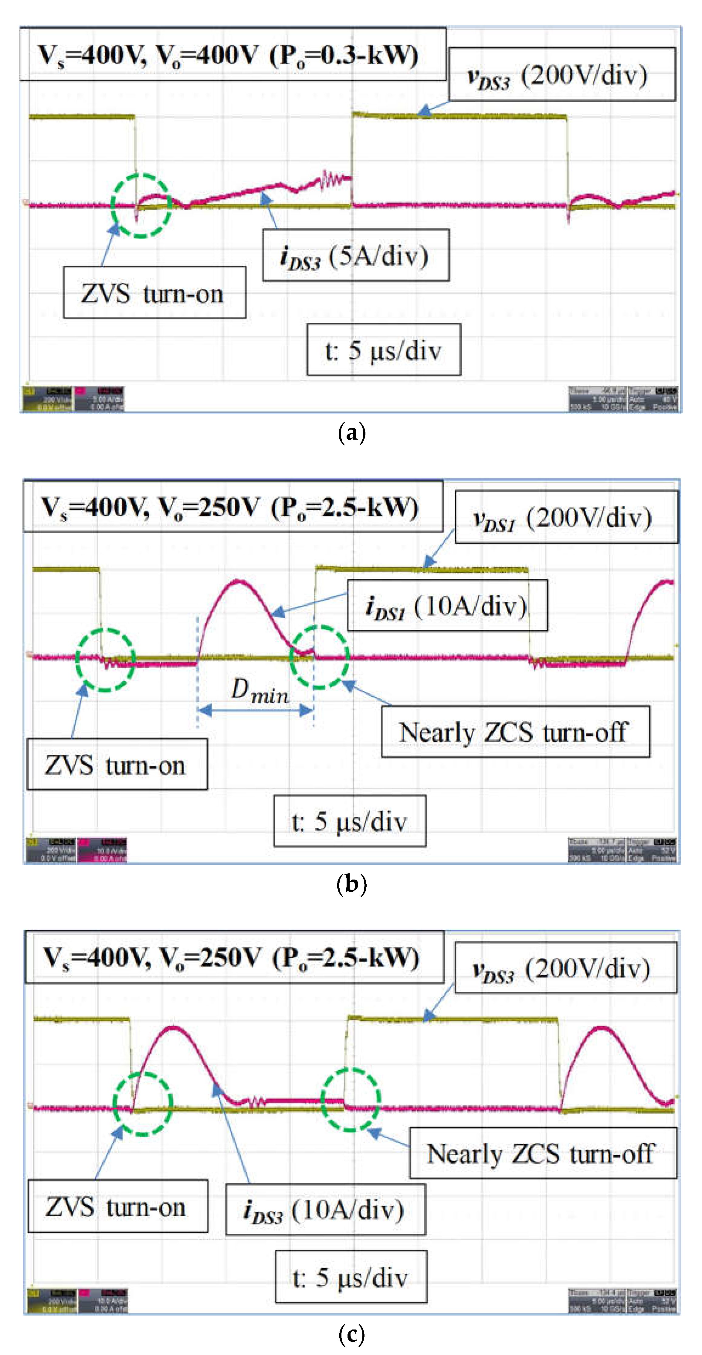
Figure 12a shows the ZVS turn-on operation of under a light-load condition at 300 W of output power. The inductive energy stored in is sufficient for discharging the output capacitor of the switches under a light-load condition. The ZVS turn-on condition of the proposed converter is independent of the load, as mentioned previously.
Figure 12b,c show the ZCS turn-off operations of and , respectively. When the input voltage is 400 V, the output voltage is 250 V (minimum value) and the load is 2.5 kW. In this case, the of is reduced to zero, and the converter operates similar to a ZCS quasi-resonant converter. becomes equal to before the leading-leg switches turn off.
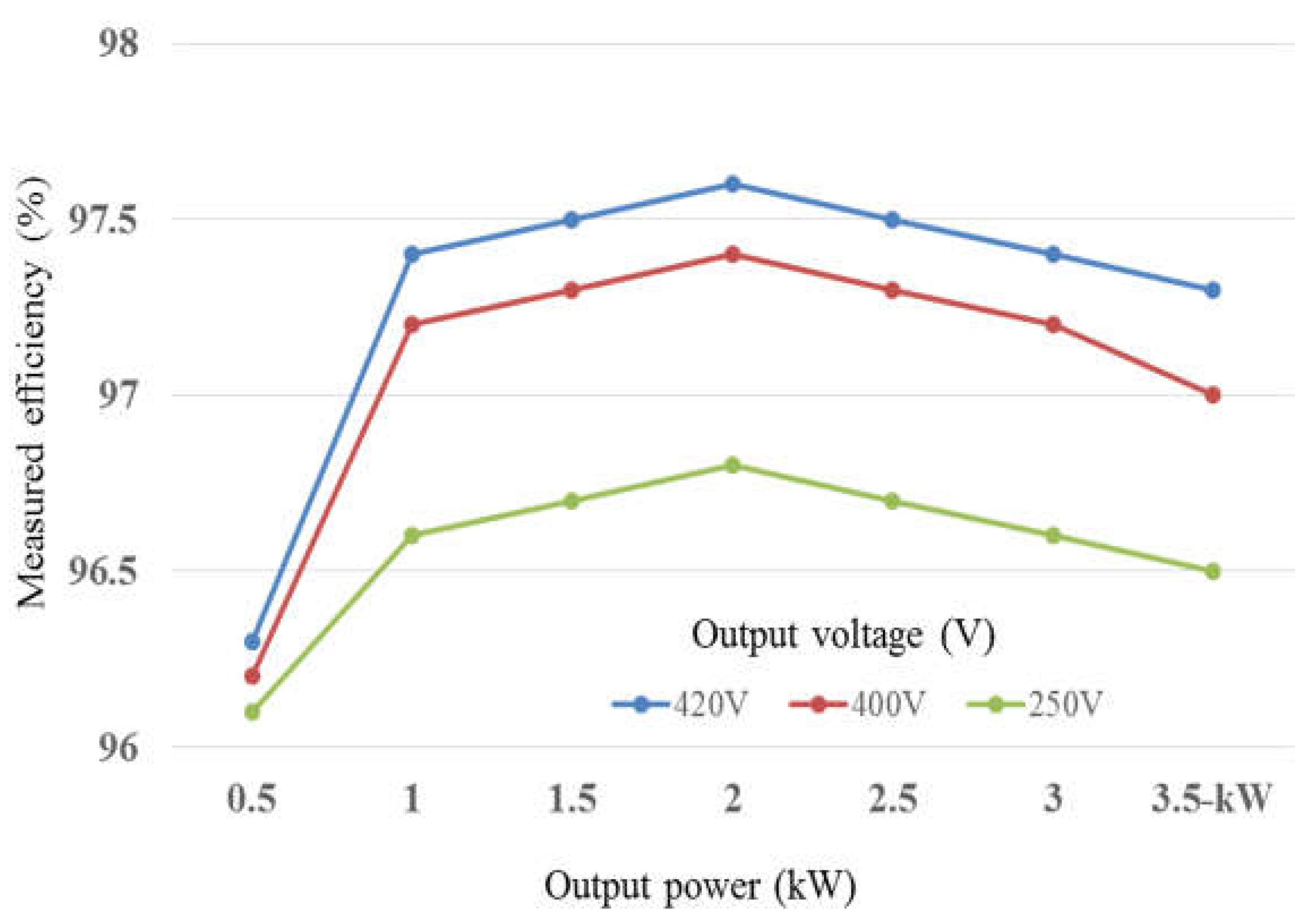
Figure 13 shows efficiency curves of the prototype converter. Efficiency curves of the prototype converter at three different output voltages of 250 V, 400 V, and 420 V over the load range between 500 W to 3.5 kW are presented. A maximum efficiency of 97.6% was achieved at an output voltage of 420 V and a 2-kW load when the input voltage was 380 V. The proposed converter exhibits high efficiency under light-load conditions (>96%).
5. Conclusions
In order to improve the performance of conventional PSFB converters, a novel quasi-resonant active-clamp circuit with a new hybrid switching scheme was introduced in the proposed method. The resonant tank is formed by the leakage inductance of the transformer and the clamping capacitor. Unlike the other control schemes with active-clamp circuits in previous research, the proposed method is capable of achieving ZVS turn-on and nearly ZCS turn-off of the primary switches over the entire load range and input voltage range. Moreover, the circulating current during the freewheeling mode and the voltage ringing across the rectifier were completely eliminated. As a result, the proposed converter can achieve high efficiency across the load range. The proposed converter is highly suitable for applications with wide variations in input voltage and load such as battery chargers and power converters for renewable energy sources.
Author Contributions
D.T. wrote the manuscript and designed the prototype of the proposed converter; N.V. analyzed the proposed converter; W.C. reviewed the manuscript and supervised the research.
Funding
This research was funded by the KEPCO (Korean Electric Power Corporation; Grant number: R17XA05-42).
Acknowledgments
This research was supported by the Korean Electric Power Corporation.
Conflicts of Interest
The authors declare no conflict of interest.
Appendix A
To derive the DC gain of the proposed converter, the dead-time intervals between and ( were neglected because they are relatively short with respect to the switching period . Therefore, the nine modes of operation ( to ) were simplified to six main modes, as shown in Figure A1.
Figure A1.
Simplified equivalent circuit model of the proposed converter. (a) Mode 2: inductor charging stage; (b) Mode 3: capacitor resonant charging stage; (c) Mode 4: inductor constant current stage; (d) Mode 5: capacitor resonant discharging stage; (e) Mode 6 (Model 8): capacitor linear discharging stage; (f) Mode 9: freewheeling stage.
Based on the simplified model in Figure 5, during half of a switching period, , the energy supplied by the input source, , is equal to the energy absorbed by the load.
where < > is the average value.
In the steady state, ; ; .
From Equation (A1), the voltage conversion ratio, M, of the proposed converter is given by
where is the average value of the secondary current .
The charge quantities , , , and are the areas under the waveform during Mode 1, Mode 2, Mode 3, and Mode 4, respectively, as shown in Figure A2.
Figure A2.
Secondary current and clamp capacitor voltage waveforms.
The first term is the triangular area, which can be calculated using Equation (A5).
Note that , from Equation (10). By substituting for from Equation (1) and Equation (2), Equation (A5) becomes
where is the normalized load, which it is defined as
The second term of Equation (A4) can be calculated as
Substituting for from Equation (13), Equation (A8) becomes
The third term of Equation (A4) can be calculated using Equation (A12).
The third term of Equation (A4) can be calculated using Equation (A11). Note that is defined as in Equation (A7).
From Equation (15), the term can be expressed as
Substituting from Equation (16), Equation (A7), and Equation (A12) into Equation (A11) gives Equation (39).
From Equation (A6), Equation (A9), Equation (A10), and Equation (A13), Equation (A4) becomes
By defining the normalized and substituting Equation (3) and Equation (A2), Equation (A14) becomes
References
- Aharon, I.; Kuperman, A. Topological overview of powertrains for battery-powered vehicles with range extenders. IEEE Trans. Power Electron. 2011, 26, 868–876. [Google Scholar] [CrossRef]
- Chen, Z.; Ji, B.; Ji, F.; Shi, L. Analysis and Design Considerations of an Improved ZVS Full-Bridge DC-DC Converter. In Proceedings of the 2010 Twenty-Fifth Annual IEEE Applied Power Electronics Conference and Exposition (APEC), Palm Springs, CA, USA, 21–25 February 2010; pp. 1471–1476. [Google Scholar]
- Chen, Z.; Liu, S.S.; Wang, Y.; Shi, L.C. Soft Switching Full-Bridge Converter with a Wide ZVS Range and Reduced Parasitic Oscillation. In Proceedings of the 2013 IEEE Energy Conversion Congress and Exposition (ECCE), Denver, CO, USA, 15–19 September 2013; pp. 5440–5447. [Google Scholar]
- Sun, C.; Li, X.D. Fast transient modulation for a step load change in a dual-active-bridge converter with extended-phase-shift control. Energies 2018, 11, 1569. [Google Scholar] [CrossRef]
- Xu, W.Z.; Chan, N.H.L.; Or, S.W.; Ho, S.L.; Chan, K.W. A new control method for a bi-directional phase-shift-controlled DC-DC converter with an extended load range. Energies 2017, 10, 1532. [Google Scholar] [CrossRef]
- Hsieh, Y.C.; Huang, C.S. Li-ion battery charger based on digitally controlled phase-shifted full-bridge converter. IET Power Electron. 2011, 4, 242–247. [Google Scholar] [CrossRef]
- Tran, D.D.; Vu, H.N.; Yu, S.; Choi, W. A novel soft-switching full-bridge converter with a combination of a secondary switch and a nondissipative snubber. IEEE Trans. Power Electron. 2018, 33, 1440–1452. [Google Scholar] [CrossRef]
- Kim, J.H.; Lee, I.O.; Moon, G.W. Integrated dual full-bridge converter with current-doubler rectifier for ev charger. IEEE Trans. Power Electron. 2016, 31, 942–951. [Google Scholar] [CrossRef]
- Kim, T.H.; Lee, S.J.; Choi, W. Design and control of the phase shift full bridge converter for the on-board battery charger of electric forklifts. J. Power Electron. 2012, 12, 113–119. [Google Scholar] [CrossRef]
- Lee, I.O.; Moon, G.W. Analysis and design of phase-shifted dual H-bridge converter with a wide ZVS range and reduced output filter. IEEE Trans. Ind. Electron. 2013, 60, 4415–4426. [Google Scholar] [CrossRef]
- Lee, I.O.; Moon, G.W. Phase-shifted PWM converter with a wide ZVS range and reduced circulating current. IEEE Trans. Power Electron. 2013, 28, 908–919. [Google Scholar] [CrossRef]
- Liu, C.; Gu, B.; Lai, J.S.; Wang, M.Y.; Ji, Y.C.; Cai, G.W.; Zhao, Z.; Chen, C.L.; Zheng, C.; Sun, P.W. High-efficiency hybrid full-bridge-half-bridge converter with shared ZVS lagging leg and dual outputs in series. IEEE Trans. Power Electron. 2013, 28, 849–861. [Google Scholar] [CrossRef]
- Pahlevaninezhad, M.; Das, P.; Drobnik, J.; Jain, P.K.; Bakhshai, A. A Novel ZVZCS full-bridge DC/DC converter used for electric vehicles. IEEE Trans. Power Electron. 2012, 27, 2752–2769. [Google Scholar] [CrossRef]
- Wu, X.K.; Xie, X.G.; Zhao, C.; Qian, Z.M. Low voltage and current stress ZVZCS full bridge DC-DC converter using center tapped rectifier reset. IEEE Trans. Ind. Electron. 2008, 55, 1470–1477. [Google Scholar] [CrossRef]
- Yilmaz, M.; Krein, P.T. Review of battery charger topologies, charging power levels, and infrastructure for plug-in electric and hybrid vehicles. IEEE Trans. Power Electron. 2013, 28, 2151–2169. [Google Scholar] [CrossRef]
- Cacciato, M.; Consoli, A. New Regenerative Active Snubber Circuit for ZVS Phase Shift Full Bridge Converter. In Proceedings of the 2011 Twenty-Sixth Annual IEEE Applied Power Electronics Conference and Exposition (APEC), Fort Worth, TX, USA, 6–11 March 2011; pp. 1507–1511. [Google Scholar]
- Chen, T.F.; Cheng, S. A Novel Zero-Voltage Zero-Current Switching Full-Bridge Pwm Converter Using Improved Secondary Active Clamp. In Proceedings of the 2006 IEEE International Symposium on Industrial Electronics, Montreal, QC, Canada, 9–13 July 2006. [Google Scholar]
- Cho, J.G.; Rim, G.H.; Lee, F.C. Zero voltage and zero current switching full bridge PWM converter using secondary active clamp. IEEE Power Electron. 1996, 13, 657–663. [Google Scholar]
- Cho, J.H.; Park, K.B.; Moon, G.W.; Youn, M.J. A Hybrid PWM Resonant Converter Suitable for Wide Input Variation. In Proceedings of the APEC 2009 Twenty-Fourth Annual IEEE Applied Power Electronics Conference and Exposition, Washington, DC, USA, 15–19 February 2009; pp. 1504–1510. [Google Scholar]
- Dudrik, J.; Trip, N.D. Soft-switching PS-PWM DC-DC converter for full-load range applications. IEEE Trans. Ind. Electron. 2010, 57, 2807–2814. [Google Scholar] [CrossRef]
- Gu, B.; Lai, J.S.; Kees, N.; Zheng, C. Hybrid-switching full-bridge DC-DC converter with minimal voltage stress of bridge rectifier, reduced circulating losses, and filter requirement for electric vehicle battery chargers. IEEE Trans. Power Electron. 2013, 28, 1132–1144. [Google Scholar] [CrossRef]
- Kim, E.H.; Kwon, B.H. Zero-voltage- and zero-current-switching full-bridge converter with secondary resonance. IEEE Trans. Ind. Electron. 2010, 57, 1017–1025. [Google Scholar] [CrossRef]
- Lee, S.H.; Park, C.Y.; Kwon, J.M.; Kwon, B.H. Hybrid-type full-bridge DC/DC converter with high efficiency. IEEE Trans. Power Electron. 2015, 30, 4156–4164. [Google Scholar] [CrossRef]
- Lee, W.J.; Kim, C.E.; Moon, G.W.; Han, S.K. A new phase-shifted full-bridge converter with voltage-doubler-type rectifier for high-efficiency PDP sustaining power module. IEEE Trans. Ind. Electron. 2008, 55, 2450–2458. [Google Scholar] [CrossRef]
- Mousavi, A.; Moschopoulos, G. A New ZCS-PWM full-bridge DC-DC converter with simple auxiliary circuits. IEEE Trans. Power Electron. 2014, 29, 1321–1330. [Google Scholar] [CrossRef]
- Seok, K.W.; Kwon, B.H. An improved zero-voltage and zero-current-switching full-bridge PWM converter using a simple resonant circuit. IEEE Trans. Ind. Electron. 2001, 48, 1205–1209. [Google Scholar] [CrossRef]
- Packnezhad, M.; Farzanehfard, H. A Fully Soft-Switched ZVZCS Full-Bridge PWM Converter. In Proceedings of the 2009 IEEE Symposium on Industrial Electronics & Applications, Kuala Lumpur, Malaysia, 4–6 October 2009; pp. 801–806. [Google Scholar]
- Tran, D.D.; Vu, H.N.; Choi, W. A Novel Quasi-Resonant ZVZCS Phase Shift Full Bridge Converter with an Active Clamp in the Secondary. In Proceedings of the 2016 IEEE 8th International Power Electronics and Motion Control Conference (IPEMC-ECCE Asia), Hefei, China, 22–26 May 2016; pp. 492–495. [Google Scholar]
Figure 1.
(a) Auxiliary current source to achieve zero-voltage switching (ZVS) of lagging-leg switches; (b) blocking-voltage source for the reset of the primary current.
Figure 1.
(a) Auxiliary current source to achieve zero-voltage switching (ZVS) of lagging-leg switches; (b) blocking-voltage source for the reset of the primary current.
Figure 2.
Two kinds of active-clamp circuits employed at the secondary side of the phase-shifted full-bridge (PSFB) converter: (a) the topology in Reference [26]; (b) the topologies in References [18,27,28].
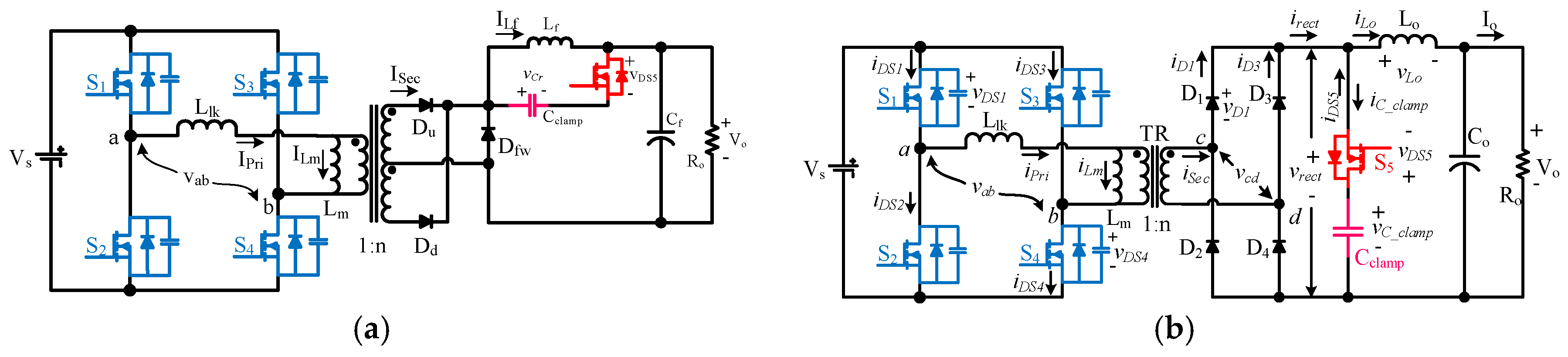
Figure 3.
Key waveforms of the proposed converter.

Figure 4.
Equivalent circuits of the proposed converter. (a) ; (b) ; (c); (d); (e); (f); (g); (h); (i); (j) ).
Figure 4.
Equivalent circuits of the proposed converter. (a) ; (b) ; (c); (d); (e); (f); (g); (h); (i); (j) ).

Figure 5.
Simplified equivalent circuit model of the proposed converter.

Figure 6.
Three-dimensional (3D) plot of the voltage gain, M, of the proposed converter when is constant.
Figure 6.
Three-dimensional (3D) plot of the voltage gain, M, of the proposed converter when is constant.

Figure 7.
Variation of the voltage gain, M, of the proposed converter depending on the duty variations at different load conditions.
Figure 7.
Variation of the voltage gain, M, of the proposed converter depending on the duty variations at different load conditions.

Figure 8.
Small duty cycle loss, minimized circulating energy, and no reverse-recovery problem in the proposed converter.
Figure 8.
Small duty cycle loss, minimized circulating energy, and no reverse-recovery problem in the proposed converter.

Figure 9.
Picture of the proposed converter.

Figure 10.
Experimental waveforms of the proposed converter at an output power of 3 kW. (a) Voltage and current waveforms of the lagging switch, ; (b) voltage and current waveforms of the leading switch, ; (c) voltage and current waveforms of the transformer; (d) voltage and current waveforms of the rectifier diode, .
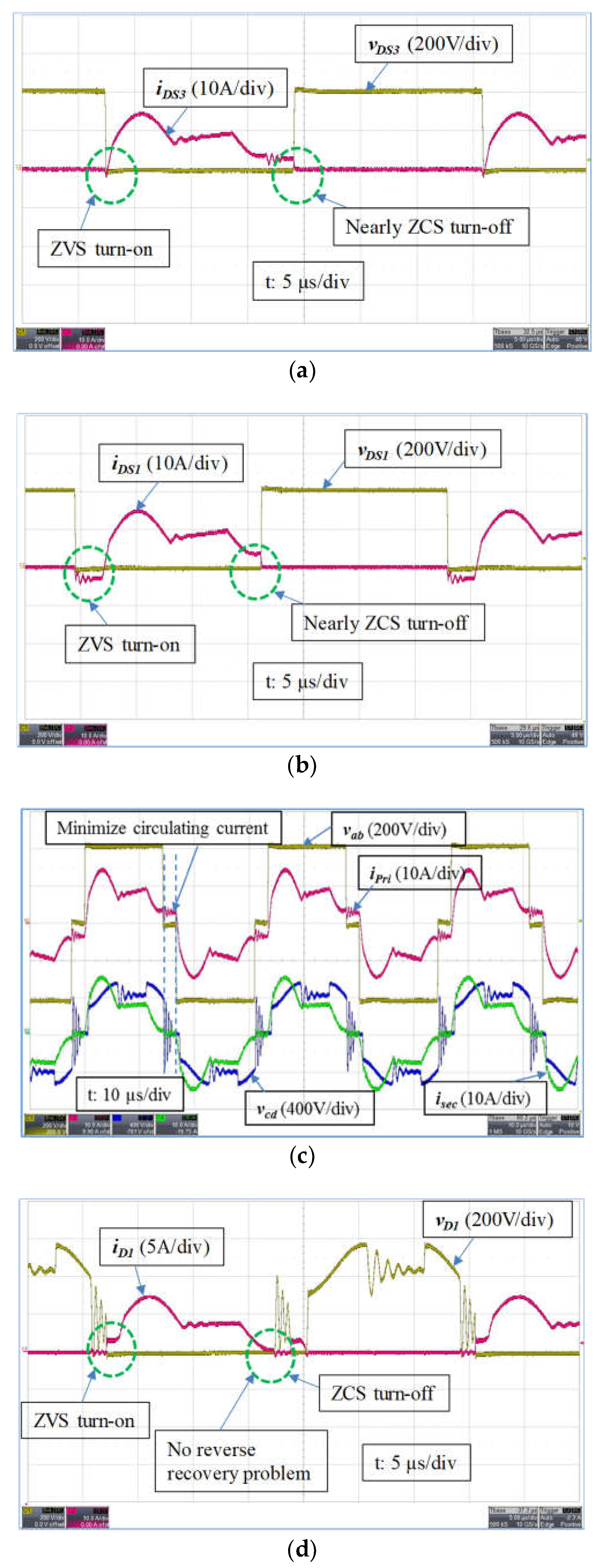
Figure 11.
Experimental waveforms of the proposed converter at an output power of 3 kW. (a) Voltage and current waveforms of the secondary active switch, ; (b) voltage and current waveforms of the clamp capacitor, .
Figure 11.
Experimental waveforms of the proposed converter at an output power of 3 kW. (a) Voltage and current waveforms of the secondary active switch, ; (b) voltage and current waveforms of the clamp capacitor, .
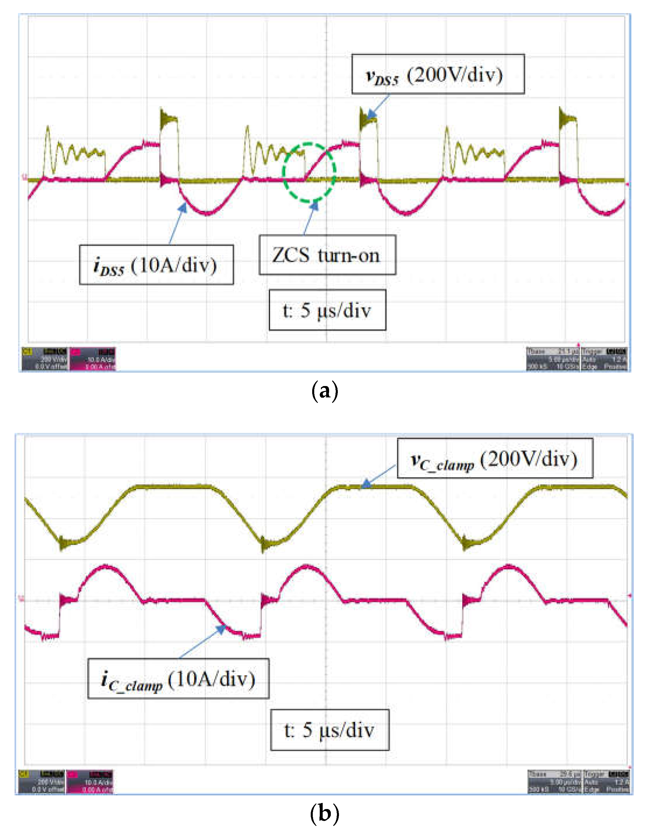
Figure 12.
Experimental waveforms of the proposed converter at light load and at minimum output voltage. (a) Voltage and current waveforms of the lagging switch, , at light load (0.3 kW); (b) voltage and current waveforms of the leading switch, , at minimum output voltage (250 V); (c) voltage and current waveforms of the lagging switch, , at minimum output voltage (250 V).

Figure 13.
Efficiency curves of the proposed converter.

Table 1.
Performance comparison of phase-shifted full-bridge (PSFB) converters with various clamp circuits. ZVS—zero-voltage switching; ZCS—zero-current switching; CDD—one capacitor and two diodes.
Table 1.
Performance comparison of phase-shifted full-bridge (PSFB) converters with various clamp circuits. ZVS—zero-voltage switching; ZCS—zero-current switching; CDD—one capacitor and two diodes.
| Type | Ref | Topology | Soft-Switching Properties | Elimination of Losses | Description of Auxiliary Circuit and Drawbacks. | |||
|---|---|---|---|---|---|---|---|---|
| ZVS Turn-On for Lagging Leg | ZCS Turn-Off for Leading Leg | Circulating Current | Reverse Recovery Current | Duty Cycle Loss | ||||
| Passive clamp [16] | [16] | Resonant CDD with 3 modes | ✔ | - | ~90% | ✔ | ✔ | - Clamp circuit: 1 capacitor and 2 diodes. - Hard-switching turn-off for leading-leg switches. |
| [13] | Resonant CDD with 1 mode | ✔ | - | ~90% | ✔ | - | - Clamp circuit: CDD type. - Hard-switching turn-off for leading-leg switches. - Duty cycle loss due to the large leakage inductance for the ZVS turn-on of the lagging leg. | |
| [14] | Modified CDD | ✔ | - | ~85% | ✔ | ✔ | - Clamp circuit: 4 diodes and 2 capacitors. - High component count for the clamp circuit. | |
| [12] | Two transformers connected in series and CDD | ✔ | - | ~60% | ✔ | ✔ | - Primary side requires 2 transformers and 1 blocking capacitor. - Low efficiency due to the transformer loss. | |
| [17] | Primary active circuit and CDD | ✔ | - | ~85% | - | ✔ | - Complex circuit: active auxiliary circuit for the ZCS turn-off of the leading leg, and passive CDD for the ZCS turn-off of the lagging leg. - Low efficiency due to the loss of the primary auxiliary circuit. | |
| [15] | Center-tapped rectifier reset | ✔ | - | ~70% | - | - | - Complex auxiliary rectifier circuits: 3 diodes, 1 inductor, and 1 capacitor to reset the primary current. - Hard-switching turn-off for the leading leg switches | |
| Active clamp | [18] [26] [27] | Standard active clamp | ✔ | - | ~85% | ✔ | - | - Hard-switching turn-off for the leading leg switches and the active-clamp switch. - ZVS condition is realized by the leakage inductance leading to a duty cycle loss. |
| [20] | Auxiliary transformer and active clamp | ✔ | - | ~85% | - | - | - Complex auxiliary circuit: a large air gap transformer, 2 voltage-divider capacitors, 4 rectifier diodes, and 1 smoothing auxiliary inductor to obtain ZVS turn-on for the leading leg switches. - High voltage rating of the secondary side components and low efficiency. | |
| [19] | Active clamp with a diode | ✔ | - | ~80% | - | - | - Use of an additional diode with the active-clamp circuit. - ZVS condition of the leading-leg switches over the entire load range cannot be guaranteed. | |
| [21] | Active clamp with a buck converter | ✔ | - | - | - | - | - Complicated active-clamp circuit: another buck converter working in discontinuous conduction mode (DCM) is required to discharge the energy stored in the clamp capacitor. - Unable to reset the circulating current at the primary side. | |
| Proposed converter | ✔ | ✔ | ~100% | ✔ | ✔ | - Same topology as Reference [20]. However, the switching scheme for the active-clamp switch is different, as shown in Table 2. - Requires control circuit for the active switch. | ||
Table 2.
Comparison of the control scheme, resonant tank, and voltage stress of the rectifier of the active-clamp circuits in Figure 2.
Table 2.
Comparison of the control scheme, resonant tank, and voltage stress of the rectifier of the active-clamp circuits in Figure 2.
| Jung-Goo’s Control [18] (1998) (Topology in Figure 2b) | Seok’s Control [26] (2001) (Topology in Figure 2a) | Mohsen’s Control [27] (2009) (Topology in Figure 2b) | Proposed Control Scheme (Topology in Figure 2b) | |
|---|---|---|---|---|
| Control schemes, primary current waveform | 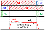 | 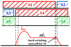 |  | 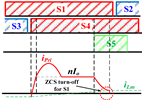 |
| Resonant tank | = 100 kHz; = 3.6 µH; = 10 µF | = 50 kHz; = 10 µH; = 47 nF | = 100 kHz; = 4.1 µH; = 10 µF | = 30 kHz; = 20 µH; = 112 nF |
| Voltage stress across the rectifier | ||||
| : switching frequency;: leakage inductor of transformer; : clamp capacitor; : primary current; : load current; n: secondary/primary transformer ratio; : source voltage | ||||
Table 3.
Design specification of the proposed converter.
| Parameter | Designator | Value |
|---|---|---|
| Input voltage nominal | 380 V | |
| Output voltage range | 250–420 V | |
| Maximum output power | 3.5 kW | |
| Switching frequency | 30 kHz | |
| Resonant frequency | 100 kHz |
Table 4.
Parameter design results.
| Parameter (Designator) | Measured Value |
|---|---|
| Turn ratio of the transformer (n1:n2) | 11:13 |
| Magnetizing inductance () | 828 µH |
| Leakage inductance () | 20 µH |
| Clamp capacitor () | 112 nF |
| Filter output inductor () | 360 µH |
Table 5.
Components used in the prototype converter.
| Component | Manufacturer | Part # |
|---|---|---|
| Primary-side switch ( | Infineon | IPW60R041C6 |
| Active-clamp switch () | Fairchild | FCH76N60N |
| Rectifier diodes ( | Vishay | HFA50PA60 |
© 2018 by the authors. Licensee MDPI, Basel, Switzerland. This article is an open access article distributed under the terms and conditions of the Creative Commons Attribution (CC BY) license (http://creativecommons.org/licenses/by/4.0/).
Share and Cite
MDPI and ACS Style
Tran, D.; Vu, N.; Choi, W. A Quasi-Resonant ZVZCS Phase-Shifted Full-Bridge Converter with an Active Clamp in the Secondary Side. Energies 2018, 11, 2868. https://doi.org/10.3390/en11112868
AMA Style
Tran D, Vu N, Choi W. A Quasi-Resonant ZVZCS Phase-Shifted Full-Bridge Converter with an Active Clamp in the Secondary Side. Energies. 2018; 11(11):2868. https://doi.org/10.3390/en11112868
Chicago/Turabian StyleTran, Duong, Nam Vu, and Woojin Choi. 2018. "A Quasi-Resonant ZVZCS Phase-Shifted Full-Bridge Converter with an Active Clamp in the Secondary Side" Energies 11, no. 11: 2868. https://doi.org/10.3390/en11112868
Note that from the first issue of 2016, this journal uses article numbers instead of page numbers. See further details here.