Theoretical and Experimental Investigation of Switching Ripple in the DC-Link Voltage of Single-Phase H-Bridge PWM Inverters


Abstract
:1. Introduction
2. Analysis of the Inverter Input Characteristics
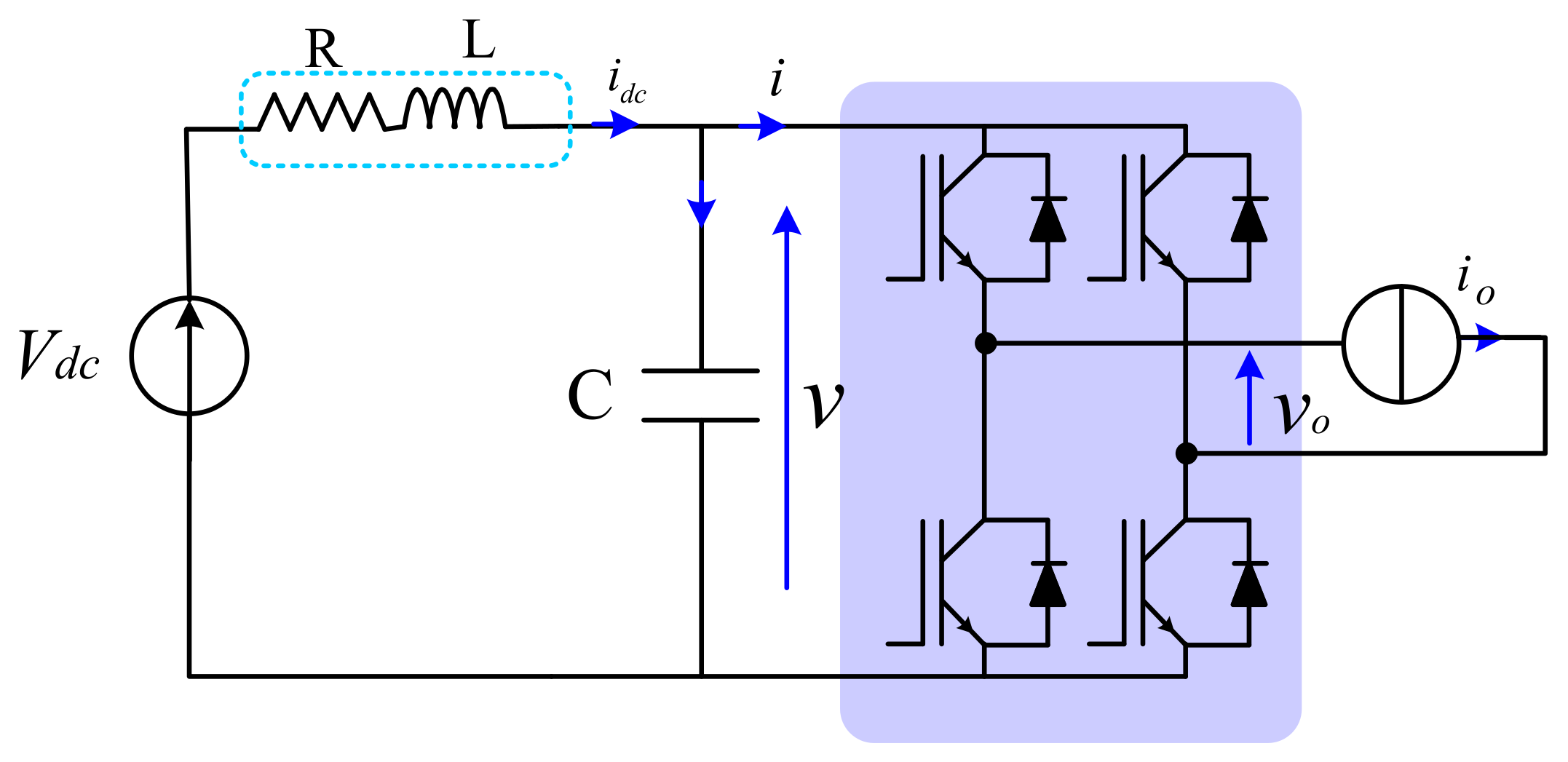
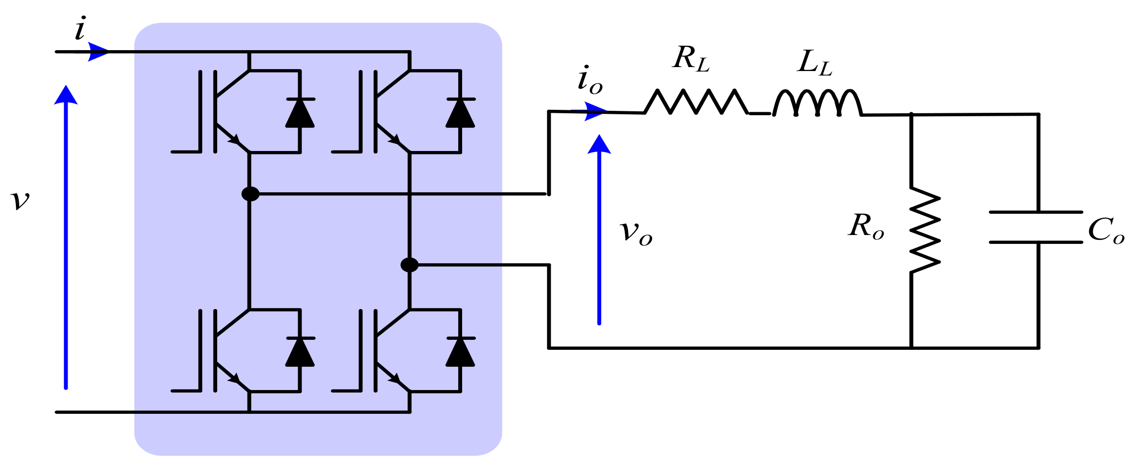
2.1. System Configuration
2.2. Input Current Analysis
3. Analysis of Input DC-Link Voltage
3.1. Low-Frequency (Averaged) DC-Link Voltage Components
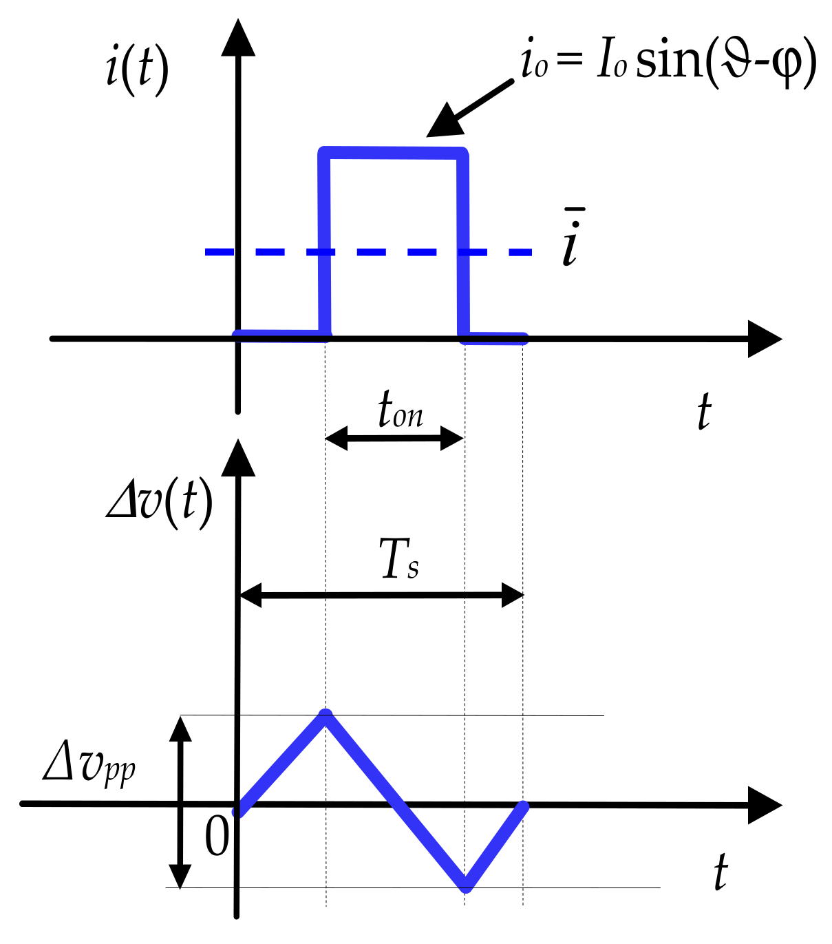
3.2. Switching Frequency DC-Link Voltage Component
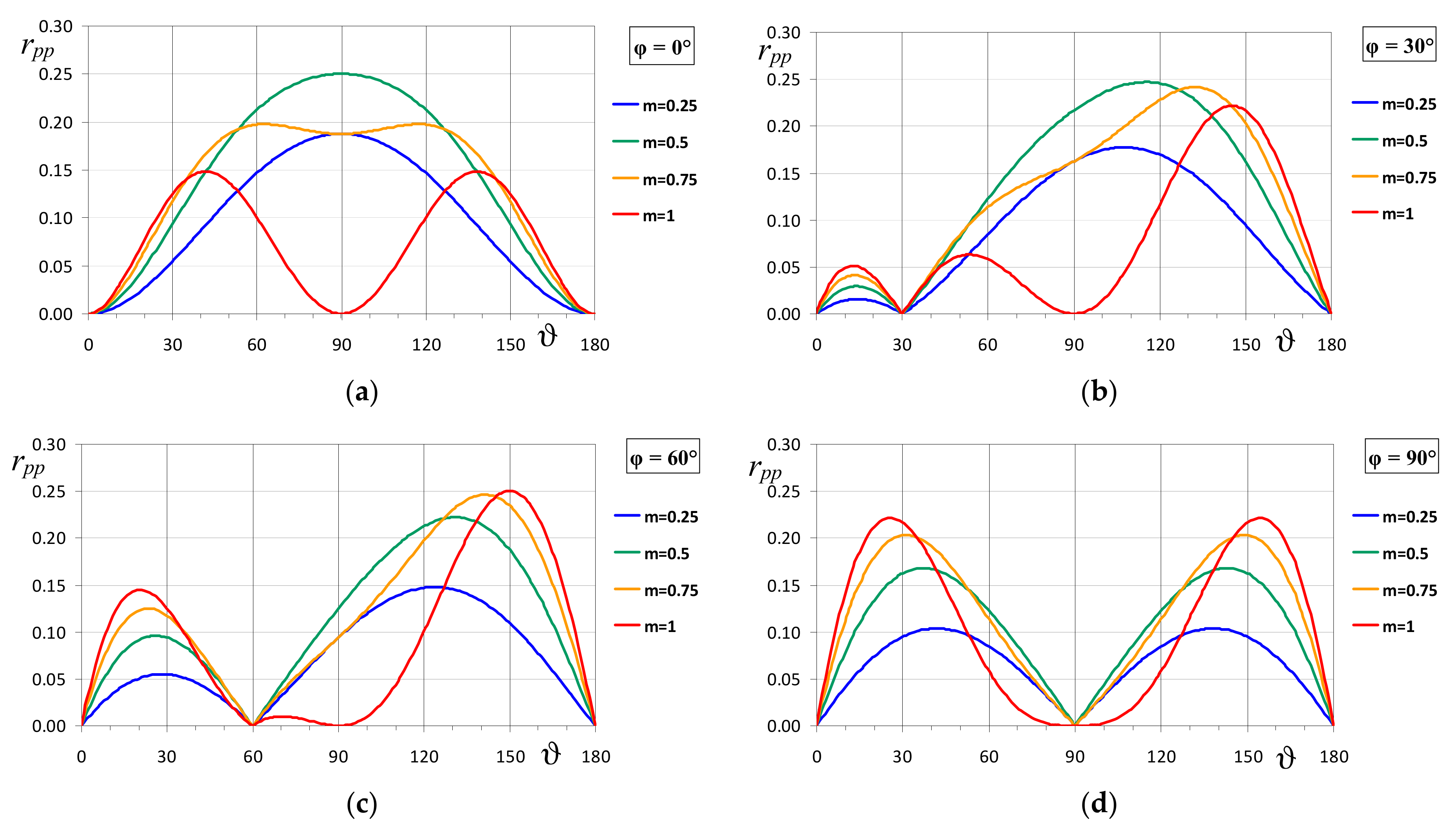
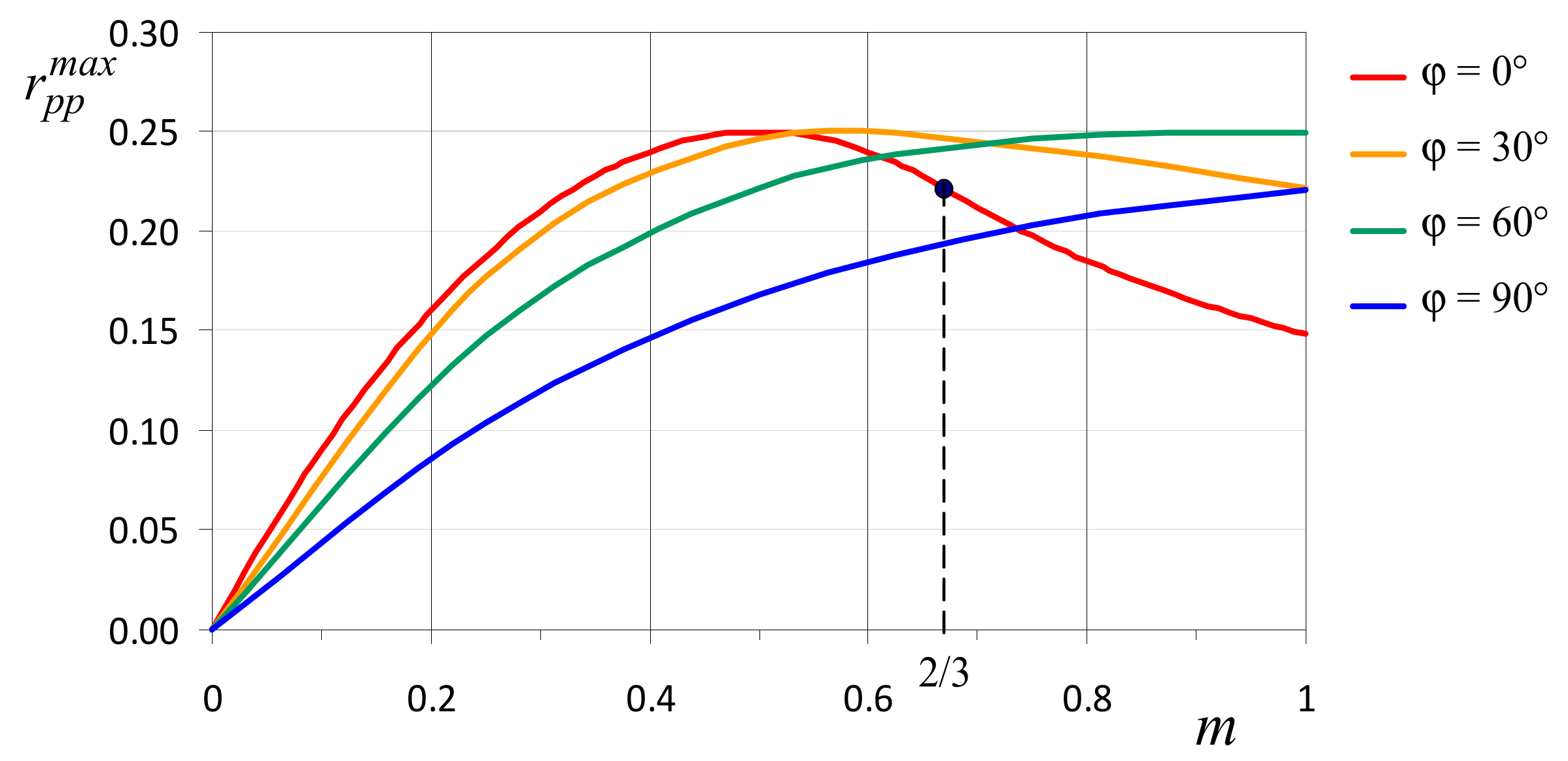
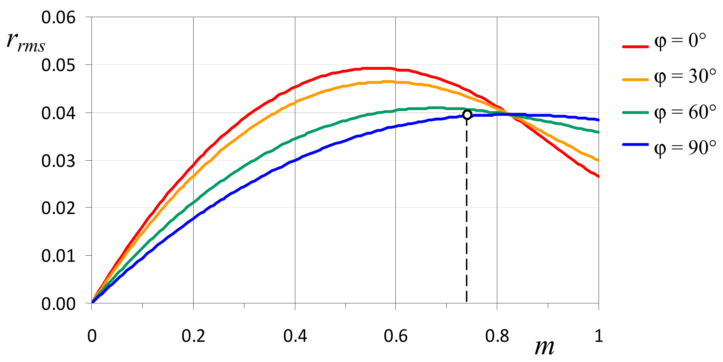
3.3. Peak-to-Peak Voltage Ripple Diagrams
3.4. RMS of Instantaneous Switching Voltage Ripple
4. Guidelines for Designing the DC-Link Capacitor
4.1. Capacitor Design Based on Switching Frequency DC-Link Voltage Ripple Requirements
4.2. Capacitor Design Based on Double-Fundamental Frequency DC-Link Voltage Ripple Requirements
4.3. Discussion
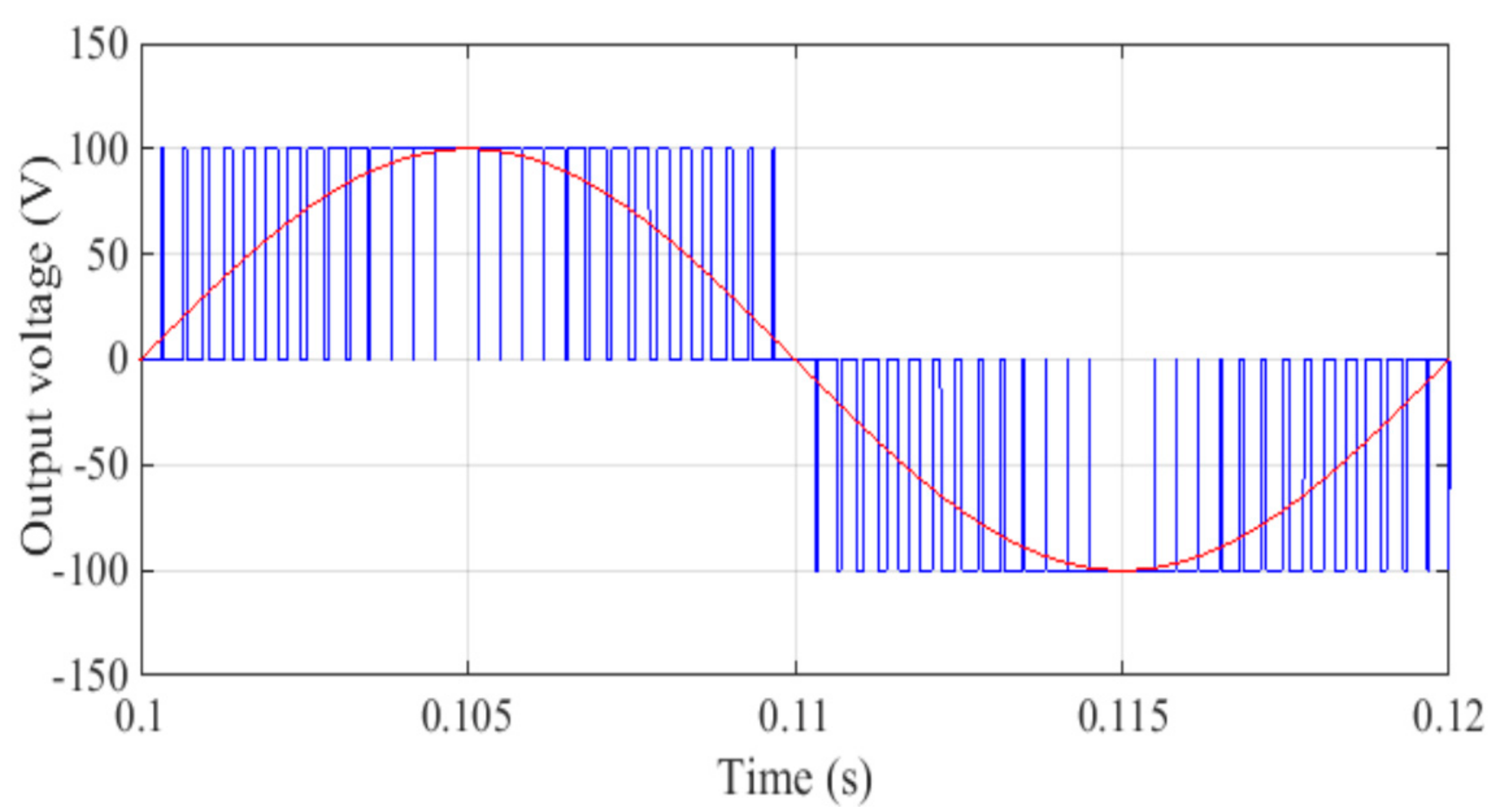
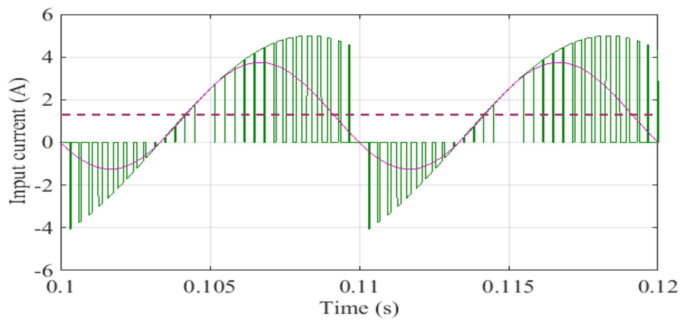
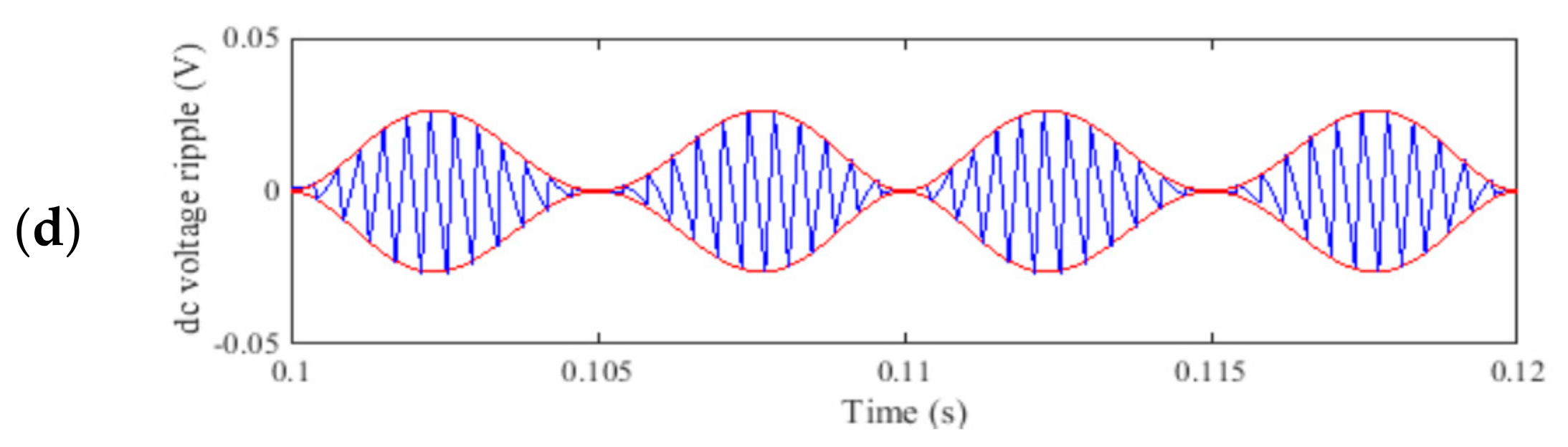
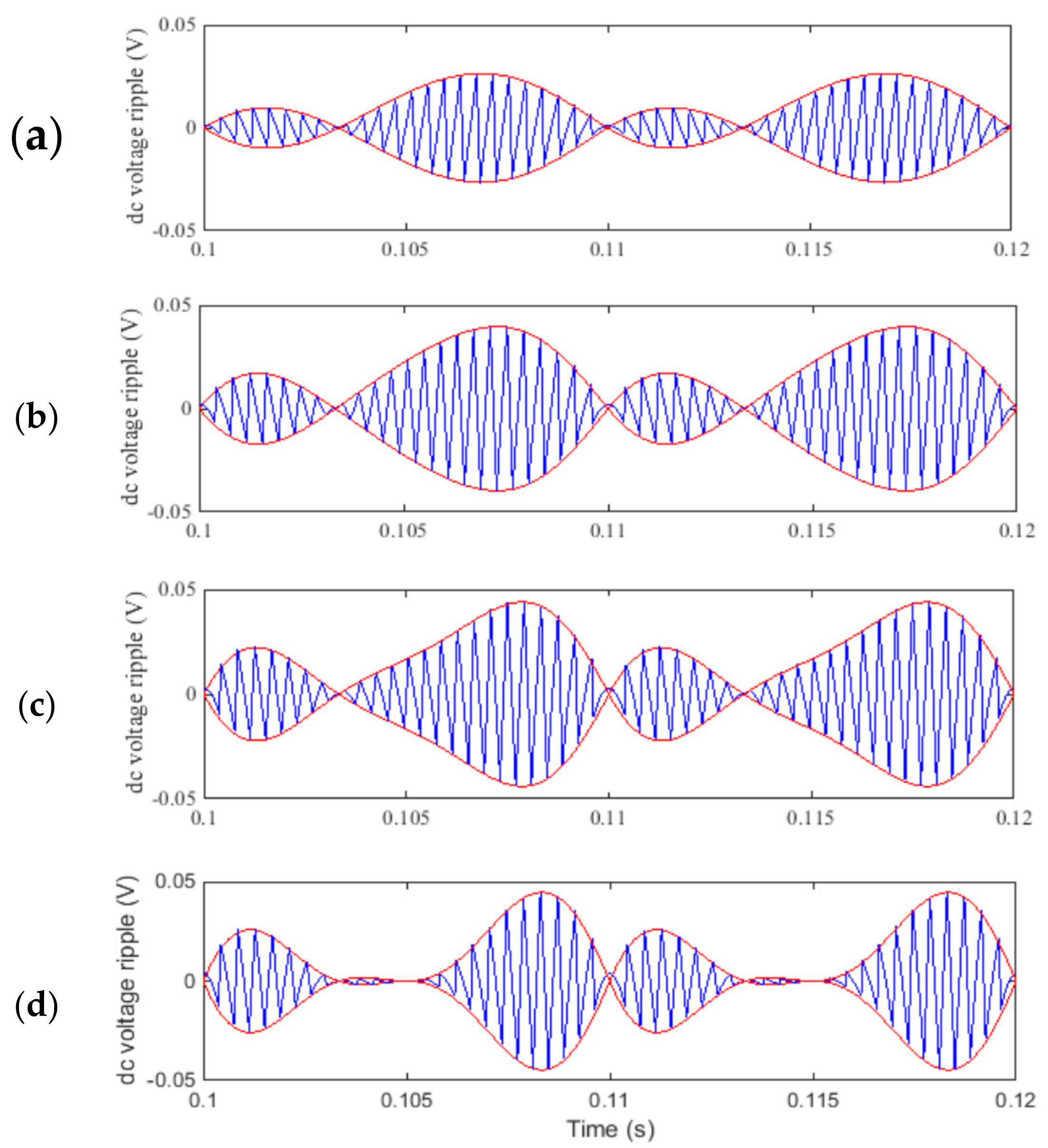
5. Numerical Results
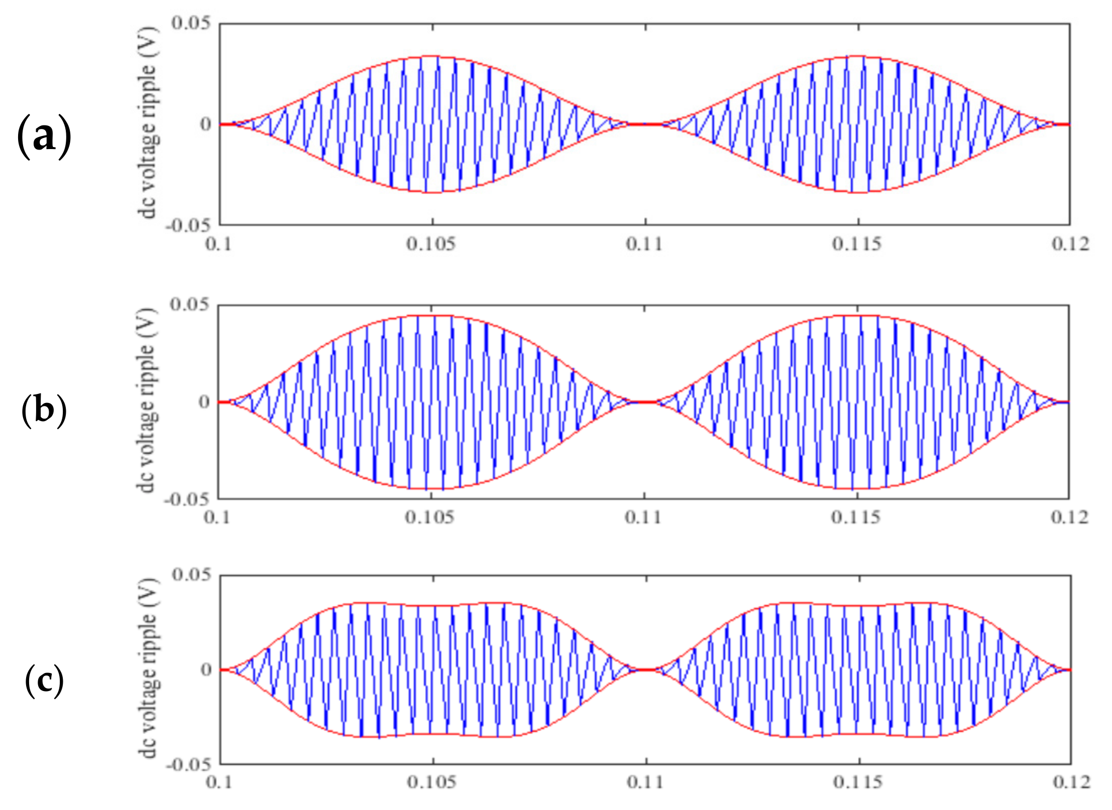
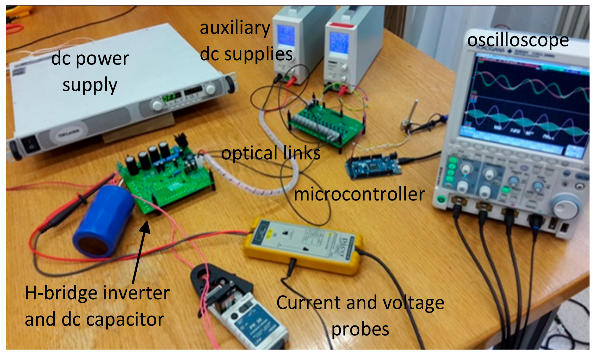
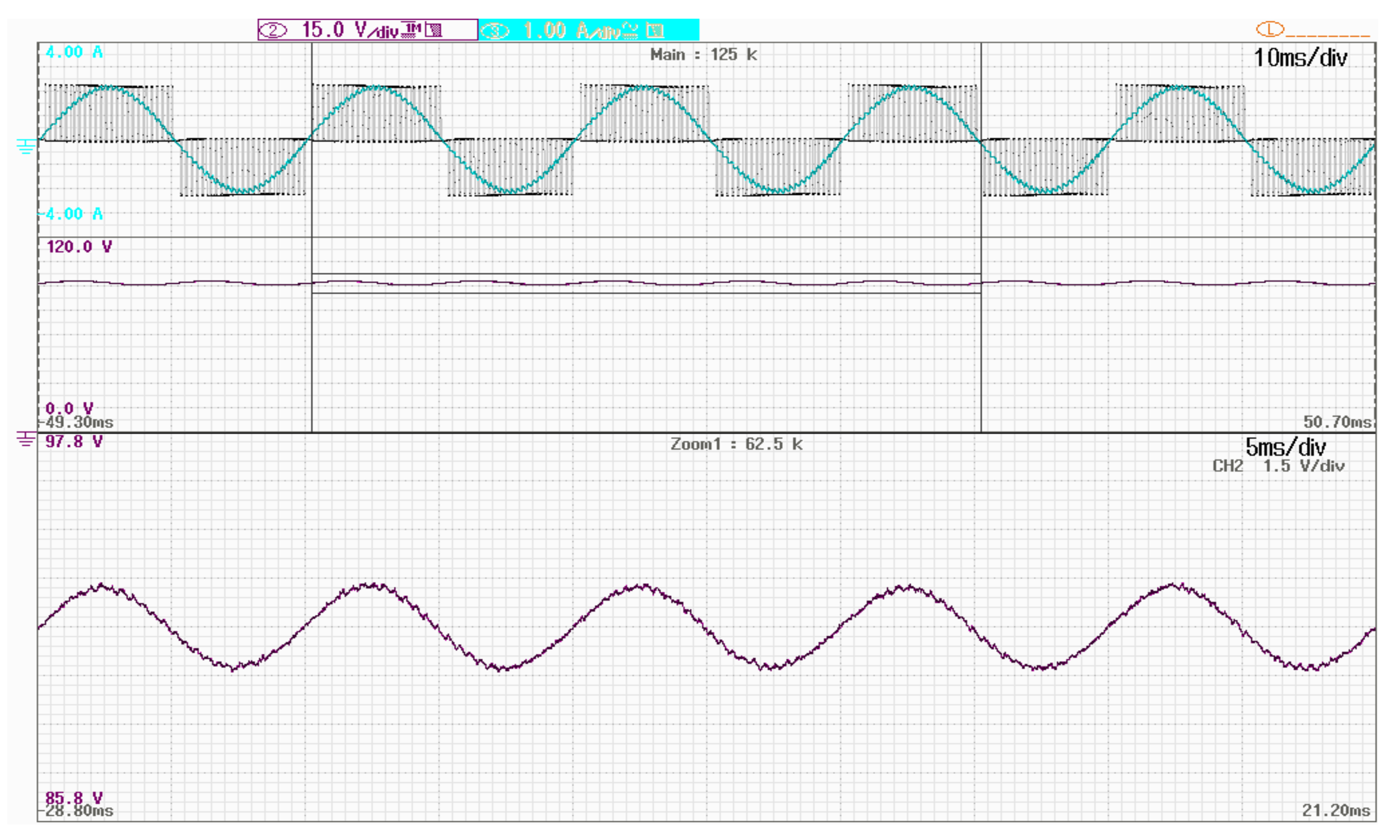
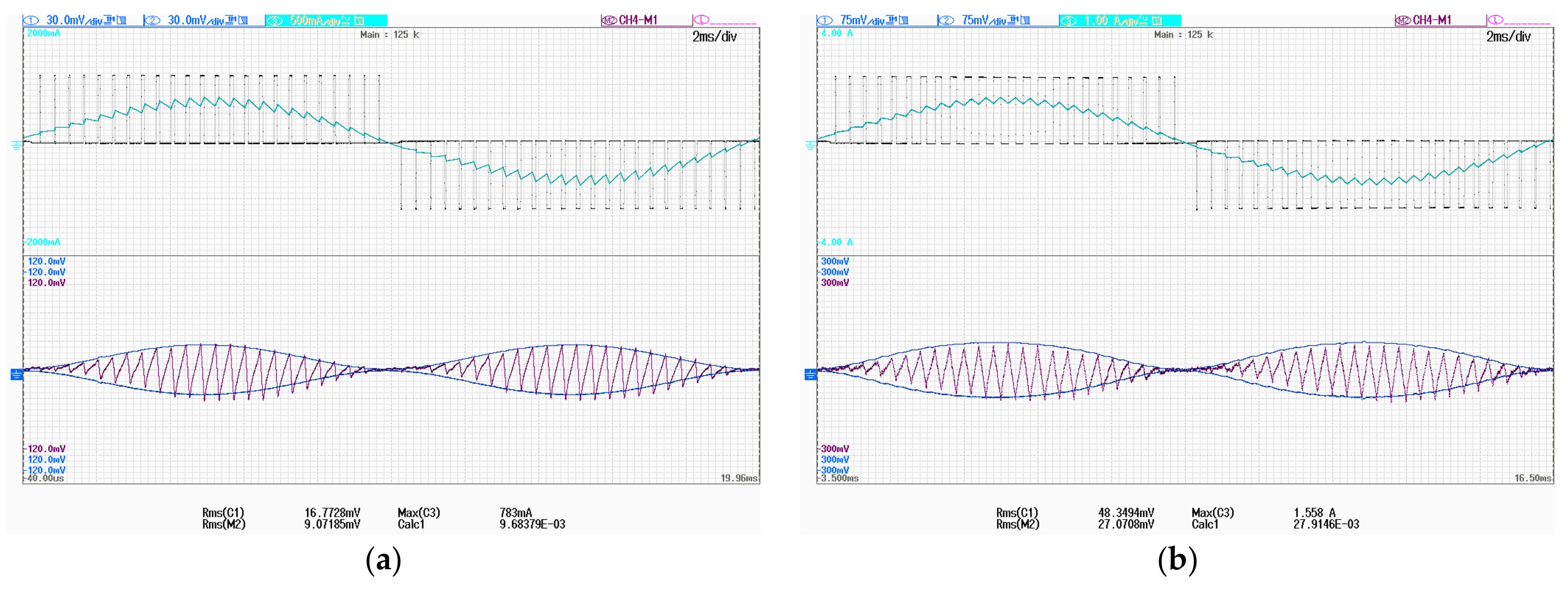
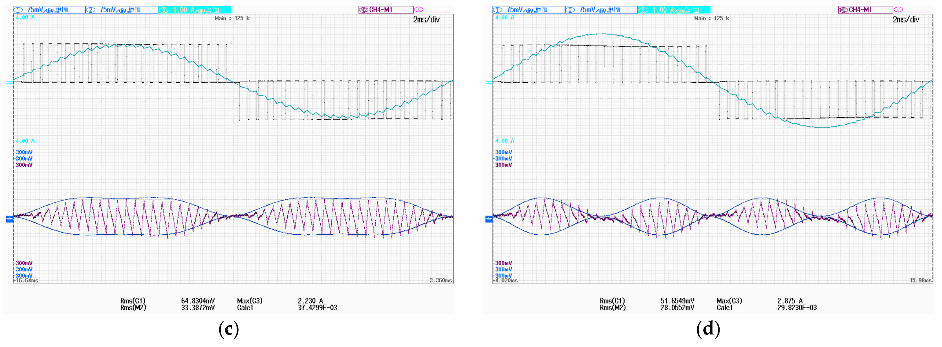
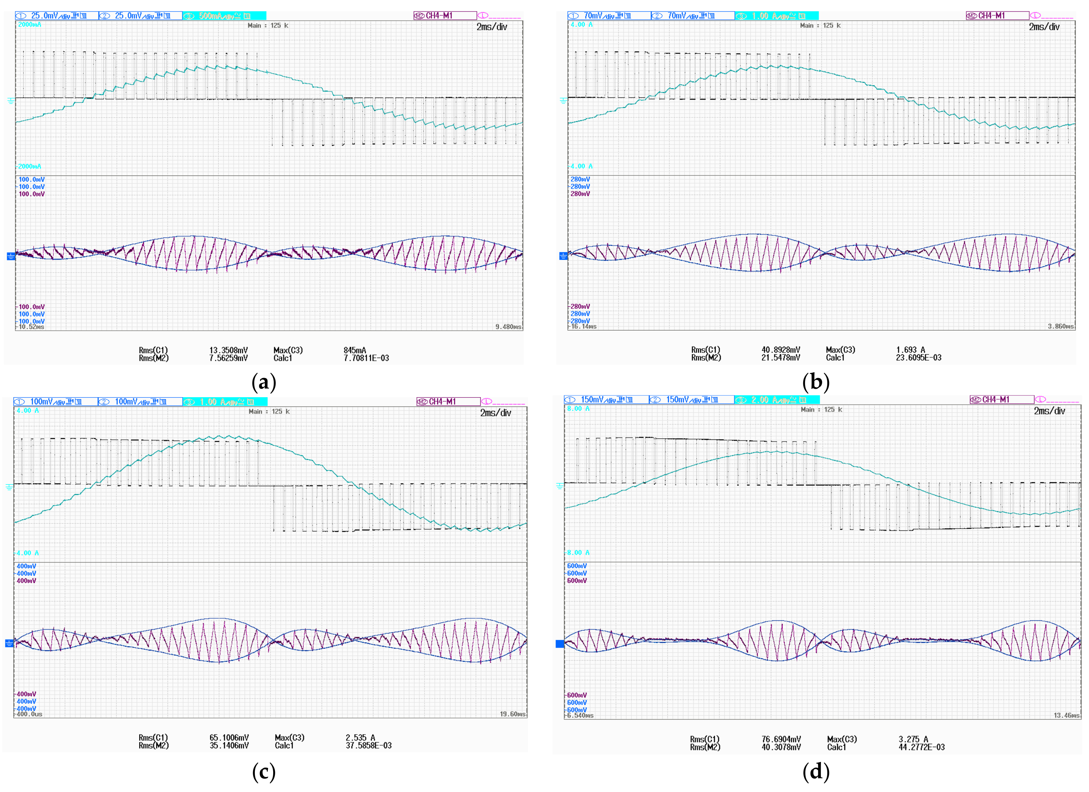
6. Experimental Results
7. Conclusions
Author Contributions
Conflicts of Interest
References
- Holmes, G.D.; Lipo, T.A. Pulse Width Modulation for Power Converters—Principles and Practice; IEEE Series on Power Engineering; John Wiley and Sons: Piscataway, NJ, USA, 2003. [Google Scholar]
- Hava, A.M.; Kerkman, R.J.; Lipo, T.A. Carrier-based PWM-VSI overmodulation strategies: Analysis, comparison, and design. IEEE Trans. Power Electron. 1998, 13, 674–689. [Google Scholar] [CrossRef]
- Zhao, D.; Hari, V.S.S.P.K.; Narayanan, G.; Ayyanar, R. Space-vector-based hybrid pulsewidth modulation techniques for reduces harmonic distorstion and switching loss. IEEE Trans. Power Electron. 2010, 25, 760–774. [Google Scholar] [CrossRef]
- Fuente, D.V.; Rodríguez, C.L.T.; Garcerá, G.; Figueres, E.; Gonzales, R.O. Photovoltaic power system with battery backup with grid-connection and islanded operation capabilities. IEEE Trans. Ind. Electron. 2013, 60, 1571–1581. [Google Scholar] [CrossRef]
- Serban, I. Power decoupling method for single-phase H-Bridge inverters with no additional power electronics. IEEE Trans. Ind. Electron. 2015, 62, 4805–4813. [Google Scholar] [CrossRef]
- Wai, R.J.; Lin, C.Y.; Huang, Y.C.; Chang, Y.R. Design of high-performance stand-alone and grid-connected inverter for distributed generation applications. IEEE Trans. Ind. Electron. 2013, 60, 1542–1555. [Google Scholar] [CrossRef]
- Grandi, G.; Loncarski, J. Evaluation of current ripple amplitude in three-phase PWM voltage source inverters. In Proceedings of the 8th IEEE Conference on Compatibility and Power Electronics (CPE), Ljubljana, Slovenia, 5–7 June 2013. [Google Scholar]
- Jiang, D.; Wang, F. Current-ripple prediction for three-phase PWM converters. IEEE Trans. Ind. Appl. 2014, 50, 531–538. [Google Scholar] [CrossRef]
- Grandi, G.; Loncarski, J.; Dordjevic, O. Analysis and comparison of peak-to-peak current ripple in two-level and multilevel PWM inverters. IEEE Trans. Ind. Electron. 2015, 62, 2721–2730. [Google Scholar] [CrossRef]
- Grandi, G.; Loncarski, J.; Rossi, C. Comparison of peak-to-peak current ripple amplitude in multiphase PWM voltage source inverters. In Proceedings of the 15th IEEE Conference on Power Electronics and Applications (EPE), Lille, France, 3–5 September 2013. [Google Scholar]
- Reznikov, B.; Srndovic, M.; Familiant, Y.L.; Grandi, G.; Ruderman, A. Simple time averaging current quality evaluation of a single-phase multilevel PWM inverter. IEEE Trans. Ind. Electron. 2016, 63, 3605–3615. [Google Scholar] [CrossRef]
- Wang, H.; Blaabjerg, F. Reliability of capacitors for DC-link applications in power electronic converters—An overview. IEEE Trans. Ind. Electron. 2014, 50, 3569–3578. [Google Scholar] [CrossRef]
- Arya, A.; Ahmad, M. W.; Agarwal, N.; Anand, S. Capacitor impedance estimation utilizing dc-link voltage oscillations in single phase inverter. IET Power Electron. 2017, 10, 1046–1053. [Google Scholar] [CrossRef]
- Kolar, J.W.; Round, S.D. Analytical calculation of the RMS current stress on the DC-link capacitor of voltage-PMW converter systems. IEE Proc. Electr. Power Appl. 2006, 153, 535–543. [Google Scholar] [CrossRef]
- Dahono, P.A.; Sato, Y.; Kataoka, T. Analysis and minimization of ripple components of input current and voltage of PWM inverters. IEEE Trans. Ind. Appl. 1996, 32, 945–950. [Google Scholar] [CrossRef]
- Gohil, G.; Bede, L.; Teodorescu, R.; Kerekes, T.; Blaabjerg, F. Analytical method to calculate the DC link current stress in voltage source converters. In Proceedings of the IEEE International Conference on Power Electronics, Drives and Energy Systems (PEDES), Mumbai, India, 16–19 December 2014. [Google Scholar]
- Wu, T.F.; Kuo, C.L.; Lin, L.C.; Chen, Y.K. DC-Bus voltage regulation for a DC distribution system with a single-phase bidirectional inverter. IEEE J. Emerg. Sel. Top. Power Electron. 2016, 4, 210–220. [Google Scholar] [CrossRef]
- Bierhoff, M.H.; Fuchs, F.W. DC-Link harmonics of three phase voltage-source converters influenced by the pulsewidth modulation strategy—An analysis. IEEE Trans. Ind. Electron. 2008, 55, 2085–2092. [Google Scholar] [CrossRef]
- McGrath, B.P.; Holmes, D.G. A general analytical method for calculating inverter DC-link current harmonics. IEEE Trans. Ind. Electron. 2009, 45, 1851–1859. [Google Scholar] [CrossRef]
- Renken, F. The DC-link capacitor current in pulsed single-phase H-bridge inverters. In Proceedings of the European Conference on Power Electronics, Dresden, Germany, 11–14 September 2005; pp. 1–10. [Google Scholar]
- Renken, F. Analytic calculation of the DC-link capacitor current for pulsed three-phase inverters. In Proceedings of the 11th International Conference on Power Electronics and Motion Control, Riga, Latvia, 2–4 September 2004. [Google Scholar]
- Pei, X.; Zhou, W.; Kang, Y. Analysis and calculation of DC-link current and voltage ripples for three-phase inverter with unbalanced load. IEEE Trans. Ind. Electron. 2015, 30, 5401–5412. [Google Scholar] [CrossRef]
- Vujacic, M.; Srndovic, M.; Hammami, M.; Grandi, G. Evaluation of DC voltage ripple in single-phase H-bridge PWM inverters. In Proceedings of the 42nd Conference of the IEEE Industrial Electronics Society, Florence, Italy, 24–27 October 2016. [Google Scholar]


| Label | Description | Parameters |
|---|---|---|
| Vdc | DC voltage supply | 96 V |
| R | DC source resistance | 5.4 Ω |
| L | DC source inductance | 19 mH |
| C | DC-link capacitance | 1.1 mF |
| fS | Switching frequency | 2.5 kHz |
| Io | Sinusoidal output current amplitude | 1 A |
| f | Fundamental frequency | 50 Hz |
| Label | Description | Parameters |
|---|---|---|
| Vdc | DC voltage supply | 96 V |
| R | DC source resistance | 5.5 Ω |
| L | DC source inductance | 19 mH |
| C | DC-link capacitance | 1.1 mF |
| fS | Switching frequency | 2.5 kHz |
| f | Fundamental frequency | 50 Hz |
| Load | ϕ = 0° | ϕ = 60° |
|---|---|---|
| RL | 4.7 Ω | 13.9 Ω |
| LL | 43.3 mH | 76.4 mH |
| Ro | 29.7 Ω | 0 |
| Co | 43.3 μF | 0 |
| m | Load Angle ϕ = 0° | Load Angle ϕ = 60° | ||||
|---|---|---|---|---|---|---|
| Theory | Sim. | Exp. | Theory | Sim. | Exp. | |
| 0.25 | 9.7 | 9.6 | 9.1 | 7.8 | 7.8 | 7.7 |
| 0.5 | 27.5 | 26.8 | 27.1 | 23.6 | 23.6 | 21.6 |
| 0.75 | 37.4 | 35.6 | 33.4 | 37.5 | 37.5 | 35.1 |
| 1.00 | 29.9 | 28.7 | 28.1 | 44.23 | 44.3 | 40.3 |
© 2017 by the authors. Licensee MDPI, Basel, Switzerland. This article is an open access article distributed under the terms and conditions of the Creative Commons Attribution (CC BY) license (http://creativecommons.org/licenses/by/4.0/).
Share and Cite
Vujacic, M.; Hammami, M.; Srndovic, M.; Grandi, G. Theoretical and Experimental Investigation of Switching Ripple in the DC-Link Voltage of Single-Phase H-Bridge PWM Inverters. Energies 2017, 10, 1189. https://doi.org/10.3390/en10081189
Vujacic M, Hammami M, Srndovic M, Grandi G. Theoretical and Experimental Investigation of Switching Ripple in the DC-Link Voltage of Single-Phase H-Bridge PWM Inverters. Energies. 2017; 10(8):1189. https://doi.org/10.3390/en10081189
Chicago/Turabian StyleVujacic, Marija, Manel Hammami, Milan Srndovic, and Gabriele Grandi. 2017. "Theoretical and Experimental Investigation of Switching Ripple in the DC-Link Voltage of Single-Phase H-Bridge PWM Inverters" Energies 10, no. 8: 1189. https://doi.org/10.3390/en10081189
APA StyleVujacic, M., Hammami, M., Srndovic, M., & Grandi, G. (2017). Theoretical and Experimental Investigation of Switching Ripple in the DC-Link Voltage of Single-Phase H-Bridge PWM Inverters. Energies, 10(8), 1189. https://doi.org/10.3390/en10081189