
A High Speed CMOS Image Sensor with a Novel Digital Correlated Double Sampling and a Differential Difference Amplifier


Abstract
:
1. Introduction
2. Correlated Double Sampling (CDS)
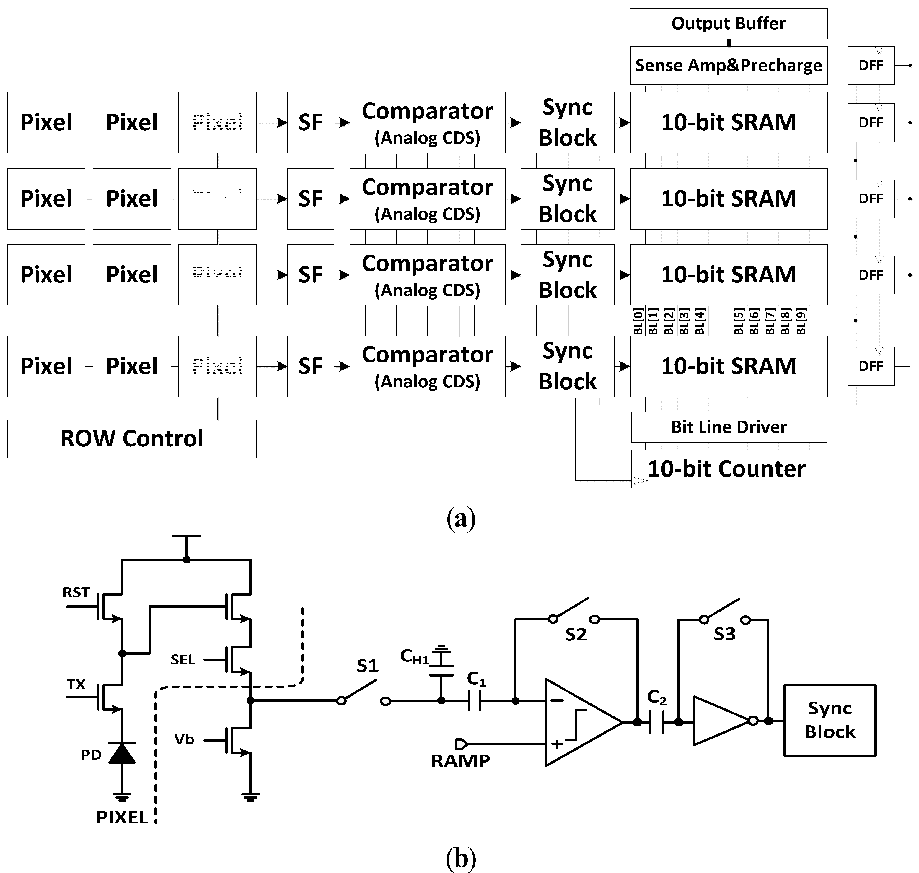
2.1. Conventional Correlated Double Sampling

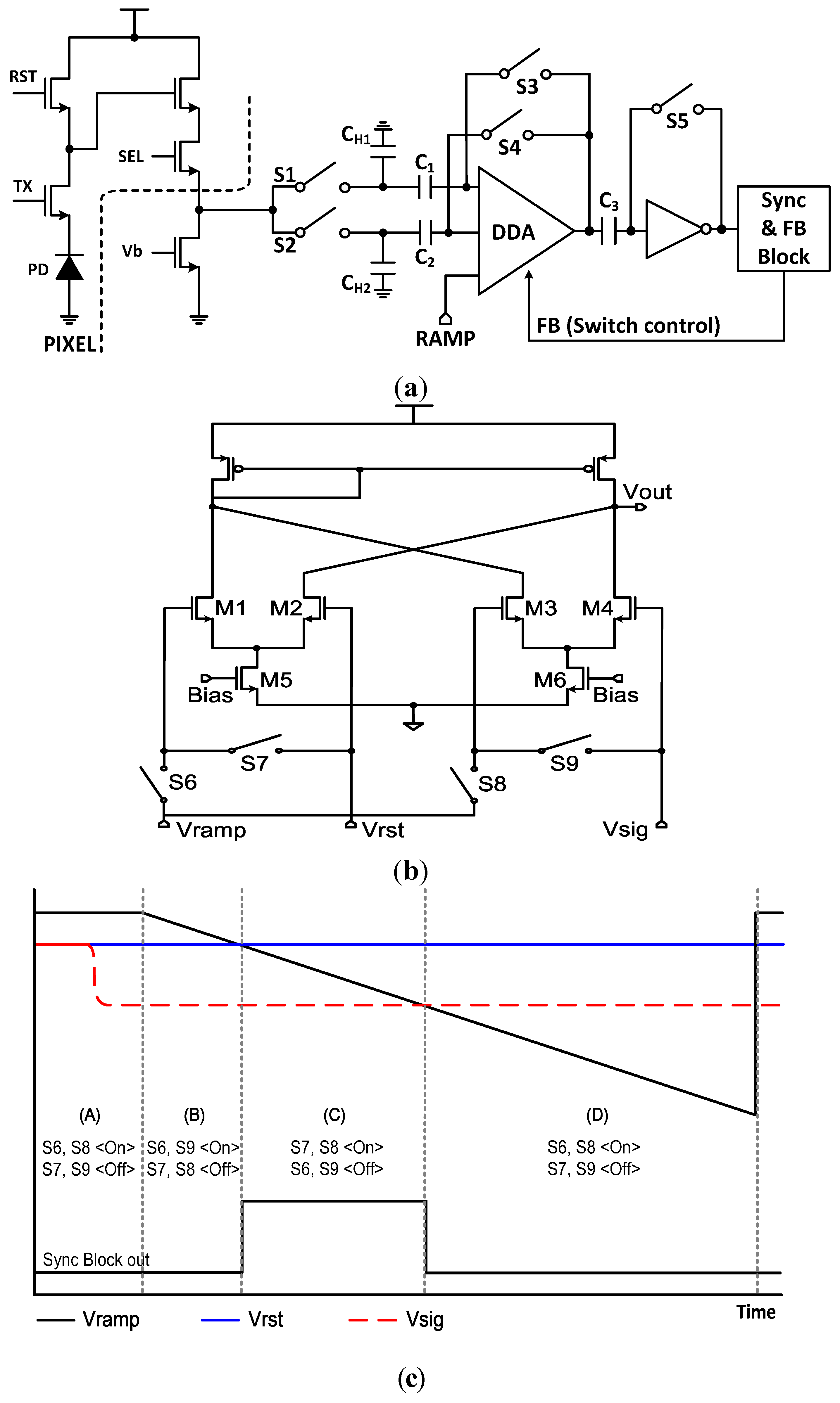
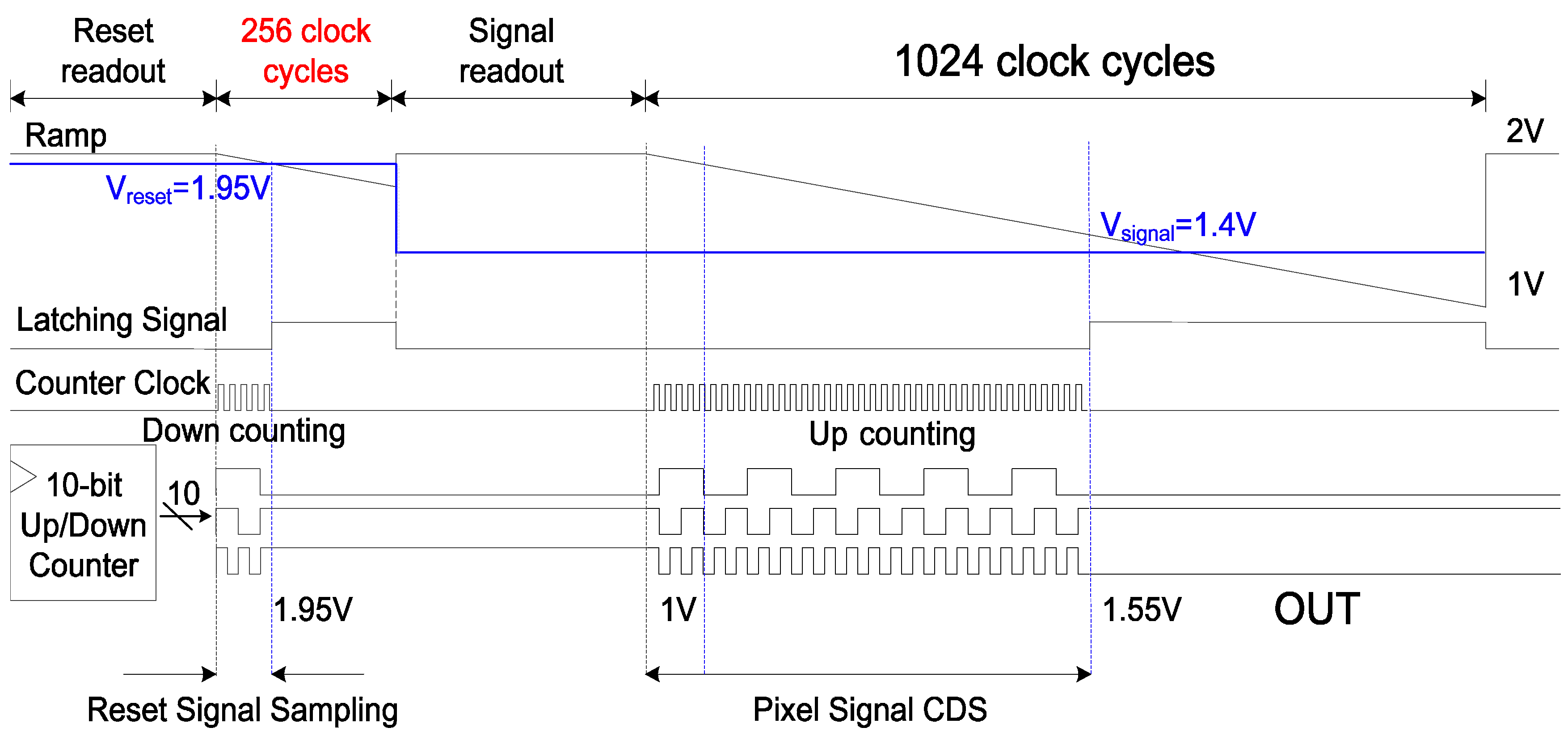
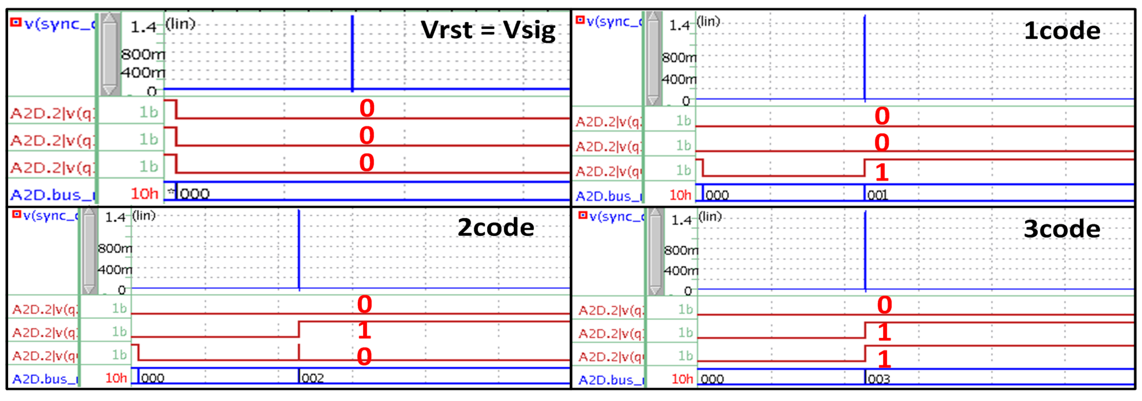
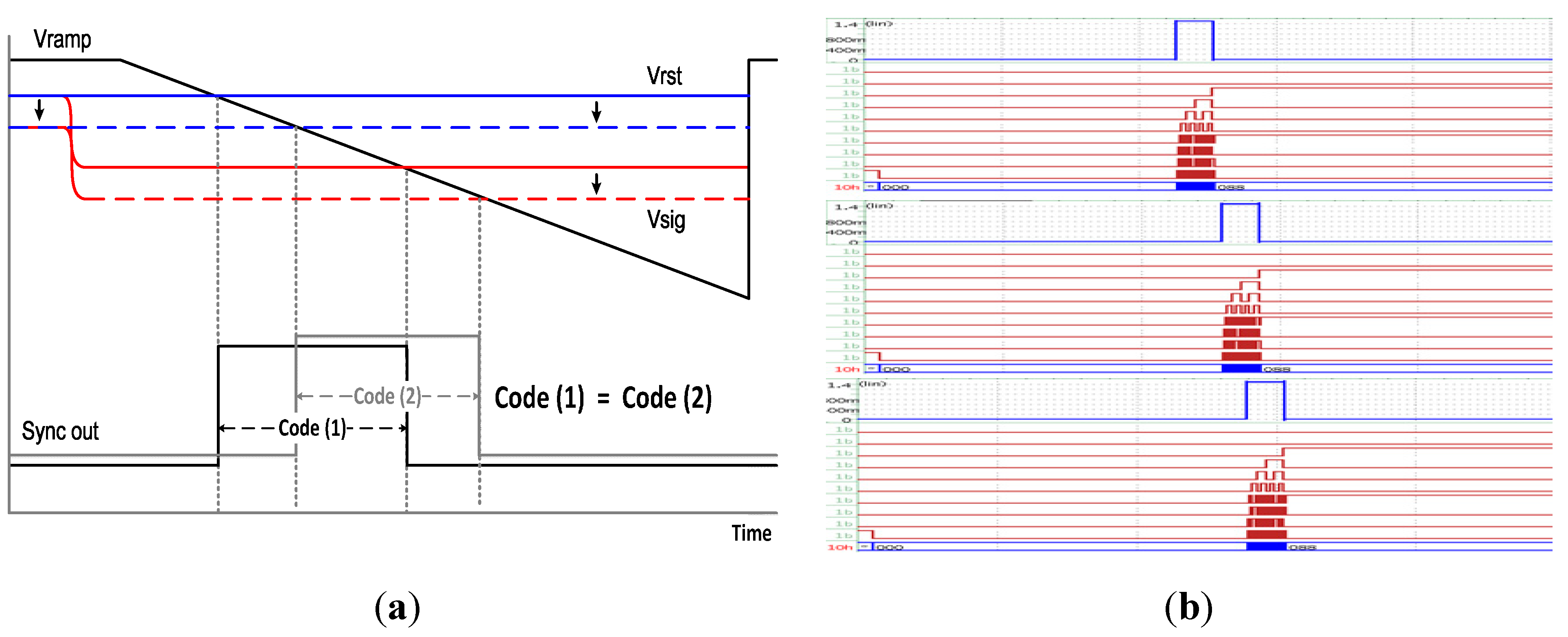
2.2. The Proposed Digital Correlated Double Sampling
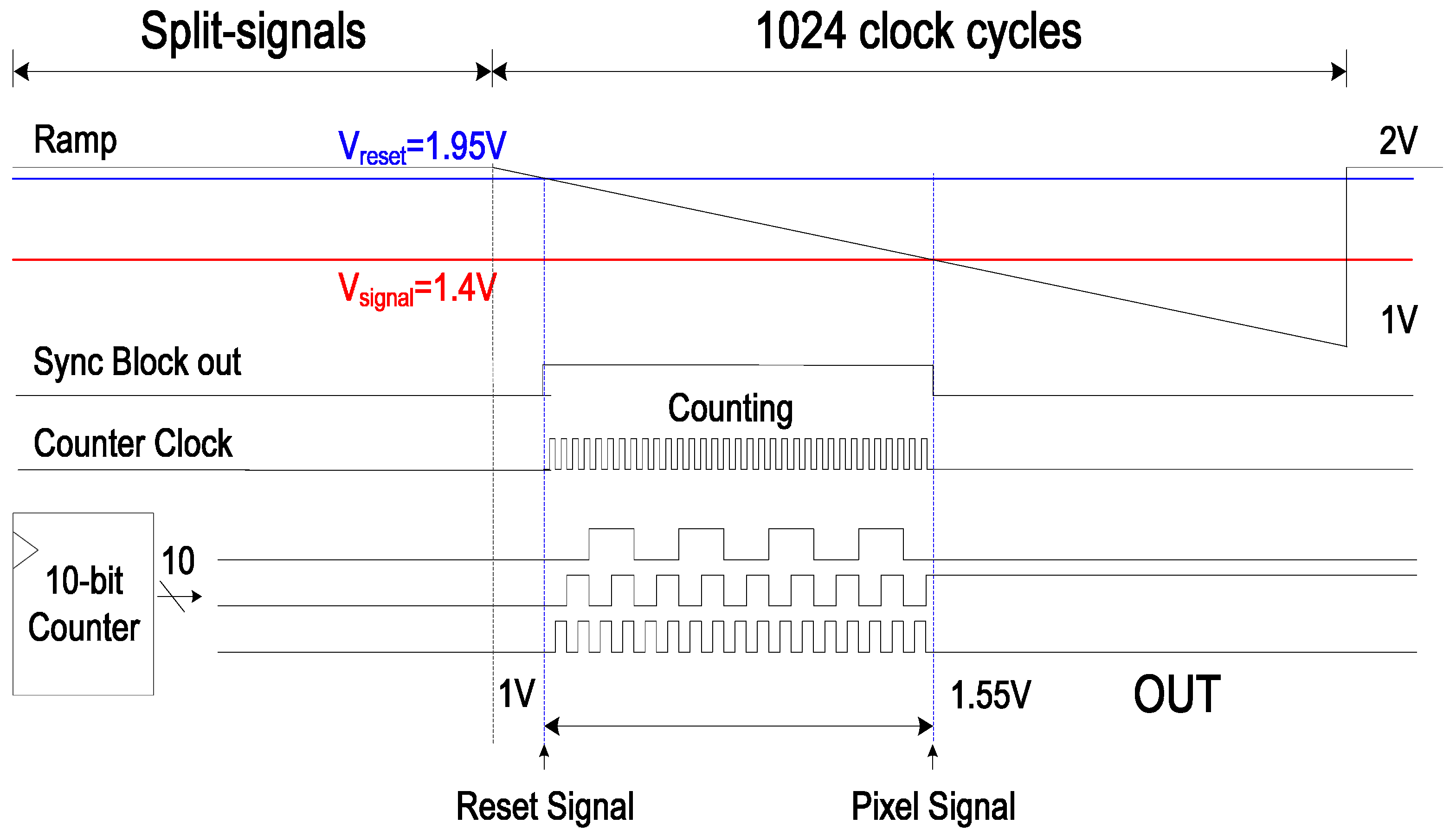
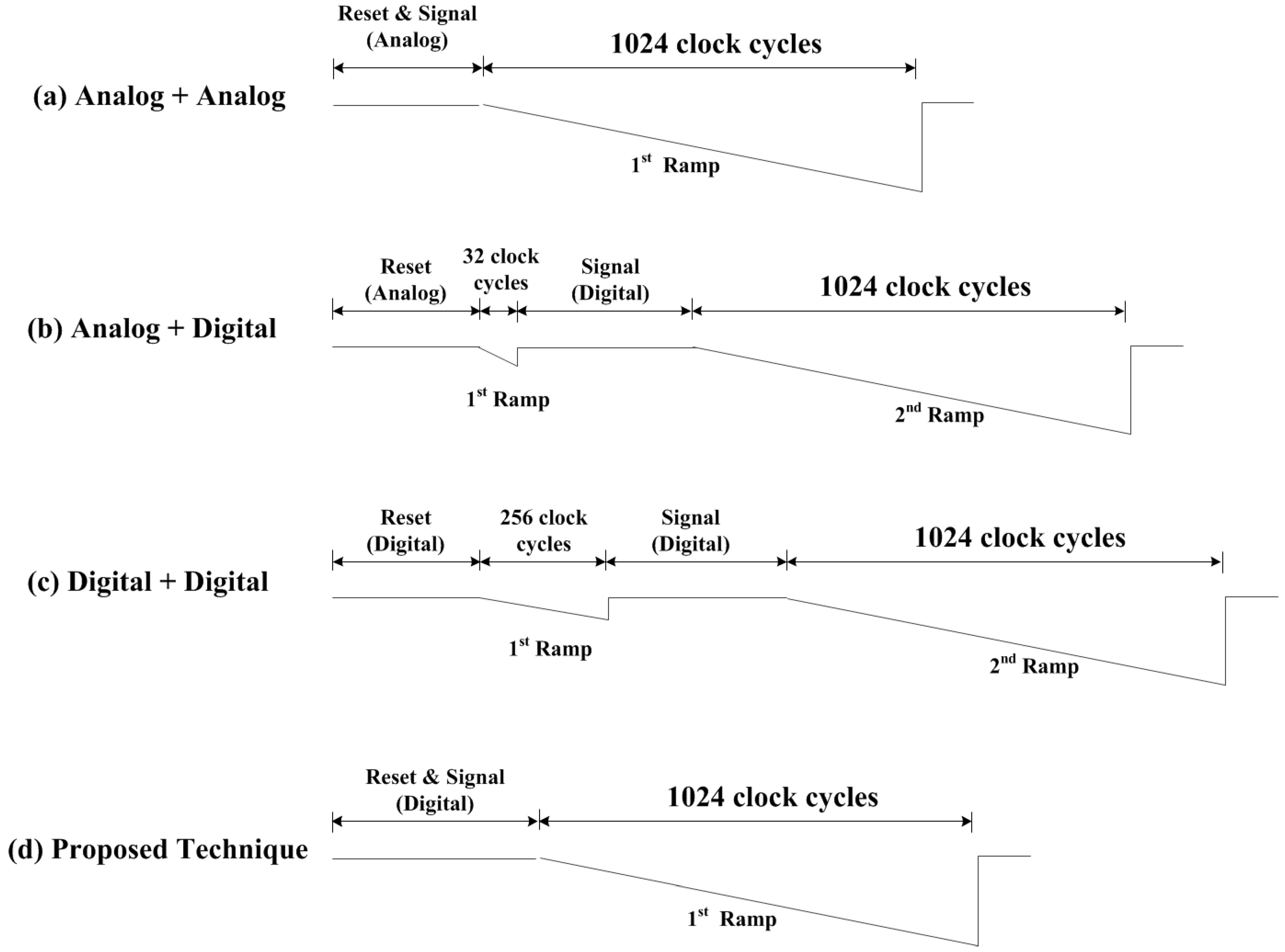
2.3. Performance Comparison among CDSs

| CDS Type (Reset + Signal) | Accuracy | Readout Time (10-bit, Ramp Cycle) | Column (µm) (11.2 um Pitch) | Power (µW) (One Column) |
|---|---|---|---|---|
| (a) Analog only | below 8-bit | 1024 | Less 323 | Less 45 |
| (b) Analog + Digital | beyond 10-bit | 32 + 1024 | 323 | 45 |
| (c) Digital + Digital | beyond 10-bit | 256 + 1024 | 450 | 51 |
| (d) Proposed Digital | beyond 10-bit | 1024 | 470 | 54 |
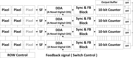
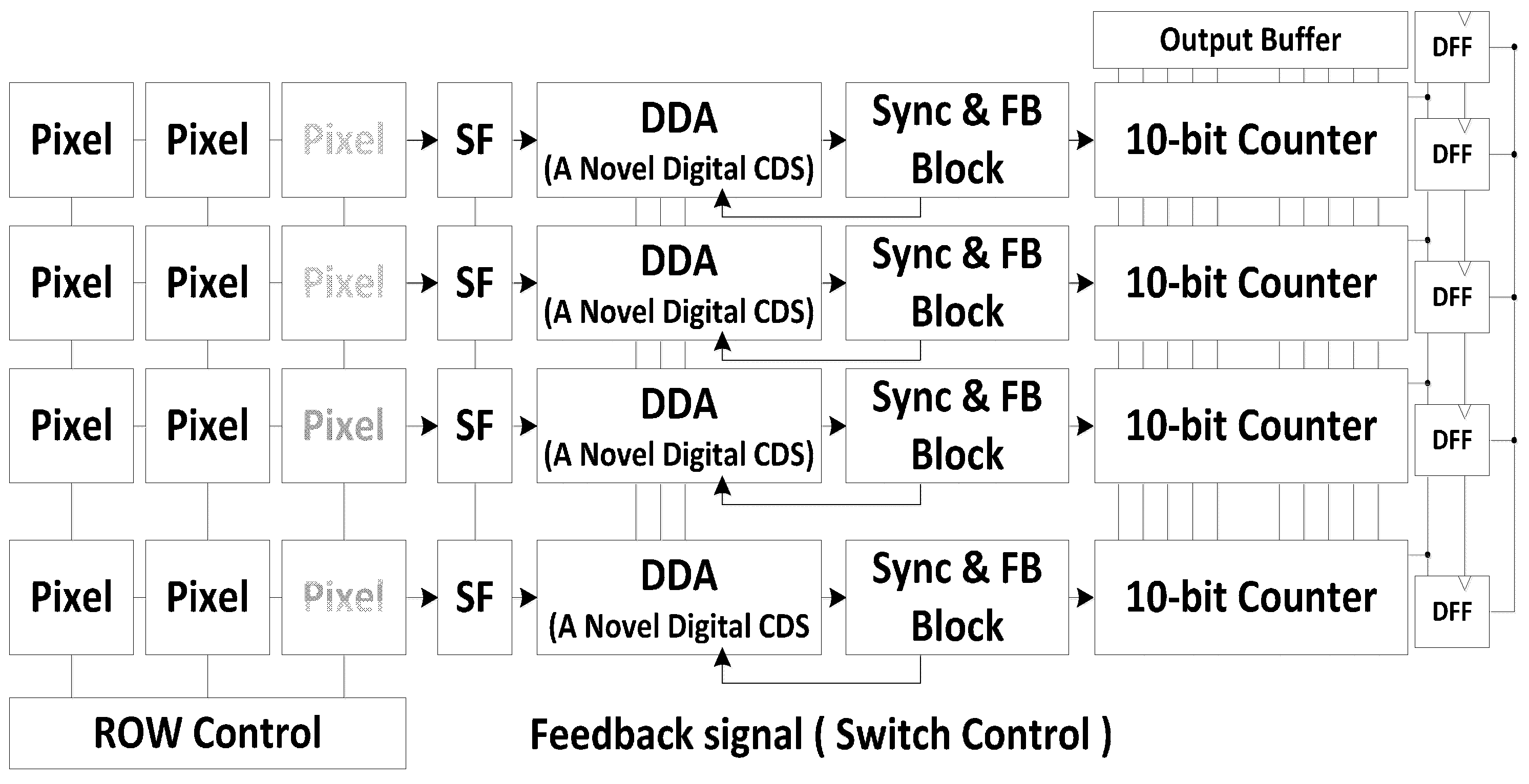
3. Circuit Implementation

| Counter | Capacitor | Total | |
|---|---|---|---|
| Conventional one (10-bit) | 330 µm (up-down) | 120 µm (1.5 pF) | 450 µm |
| This work (10-bit) | 230 µm (normal) | 240 µm (3 pF) | 470 µm |
| Column pitch = 11.2 µm, C1 = C2 = 500 fF , CH1 = CH2 = 1 pF Unit capacitor = 50 fF (L = 7 µm, W = 4 µm) | |||

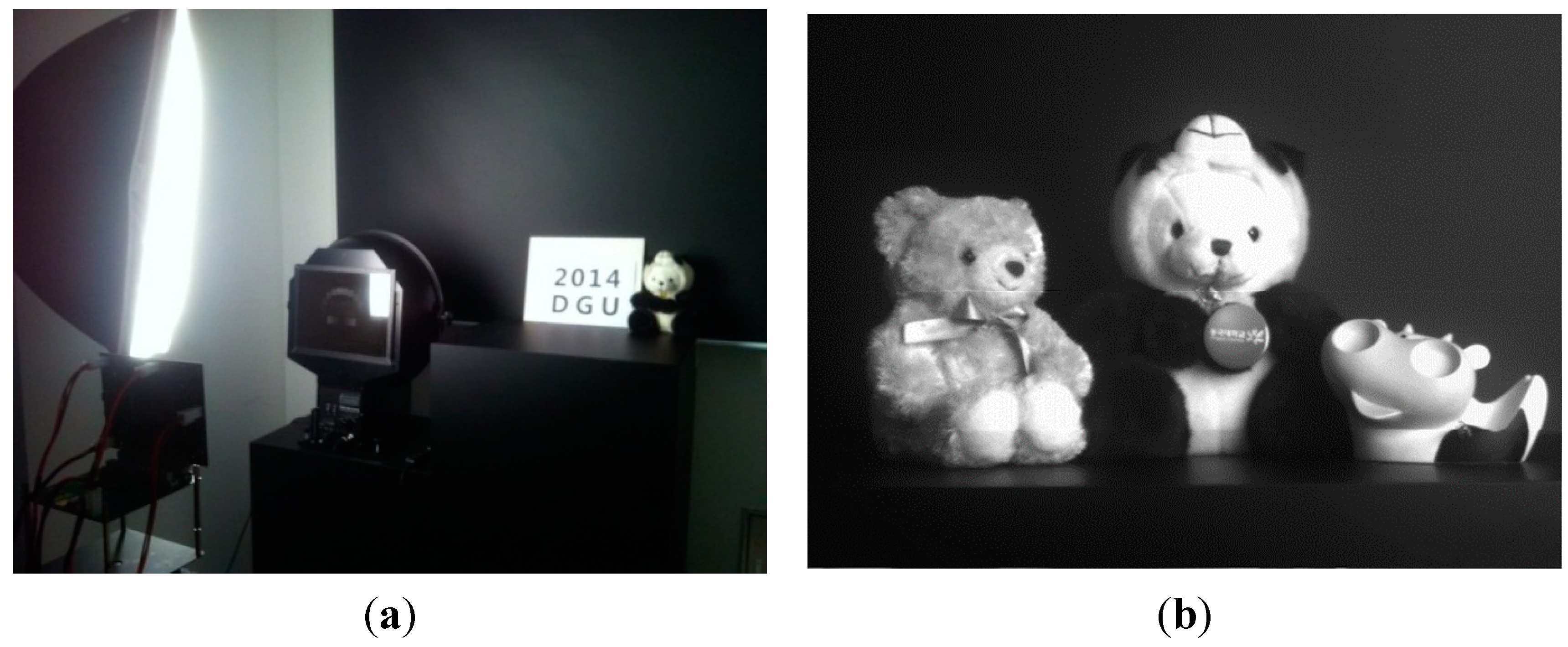
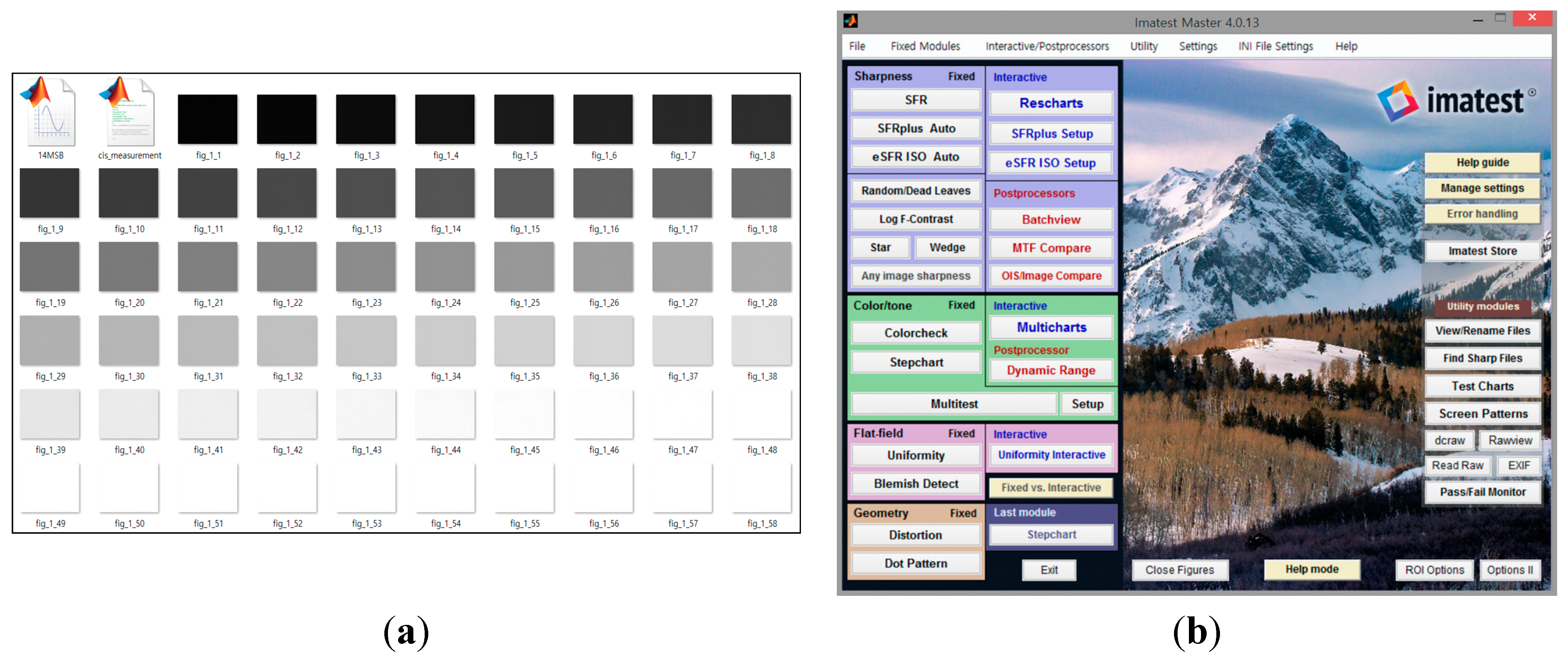
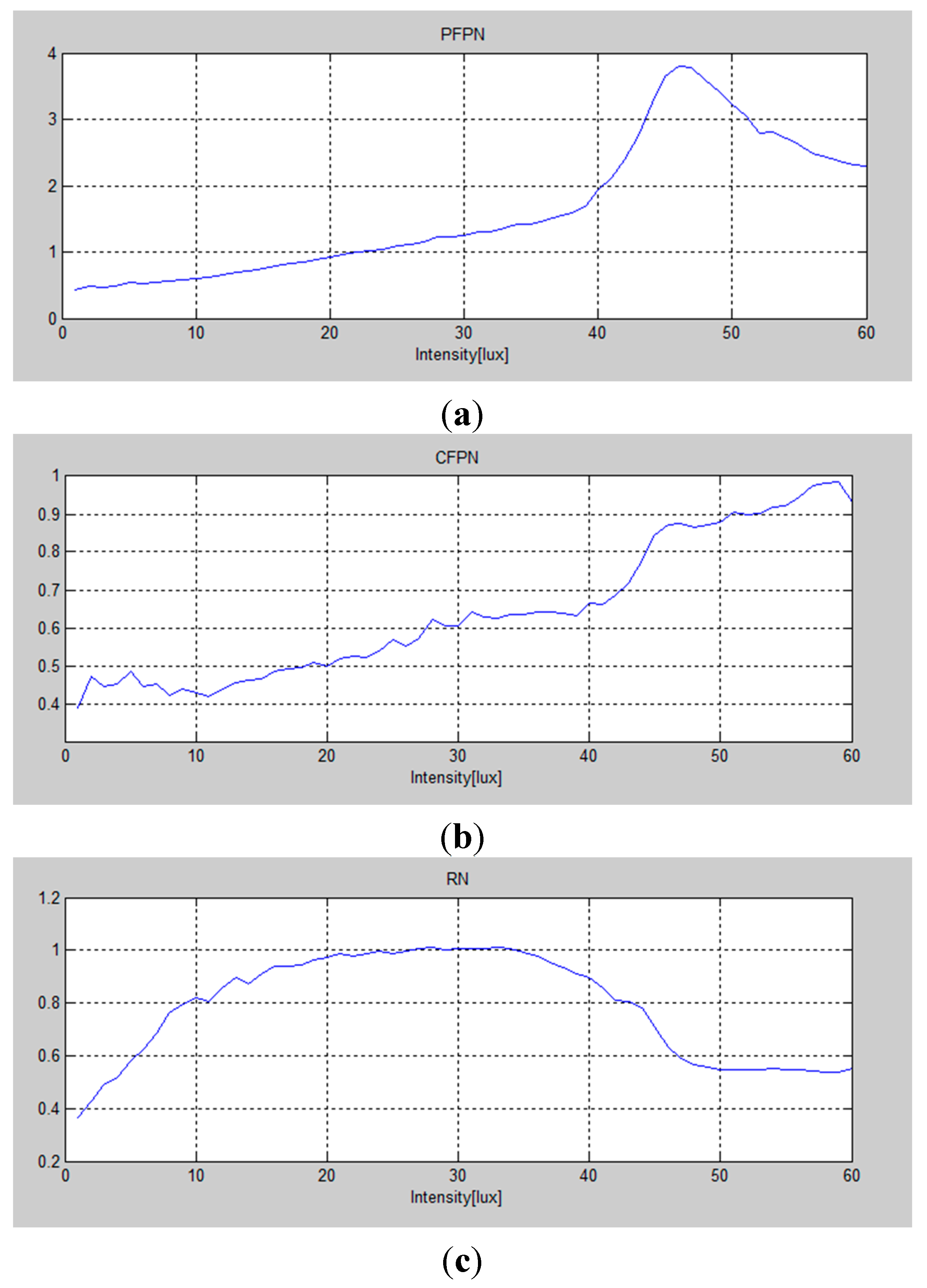
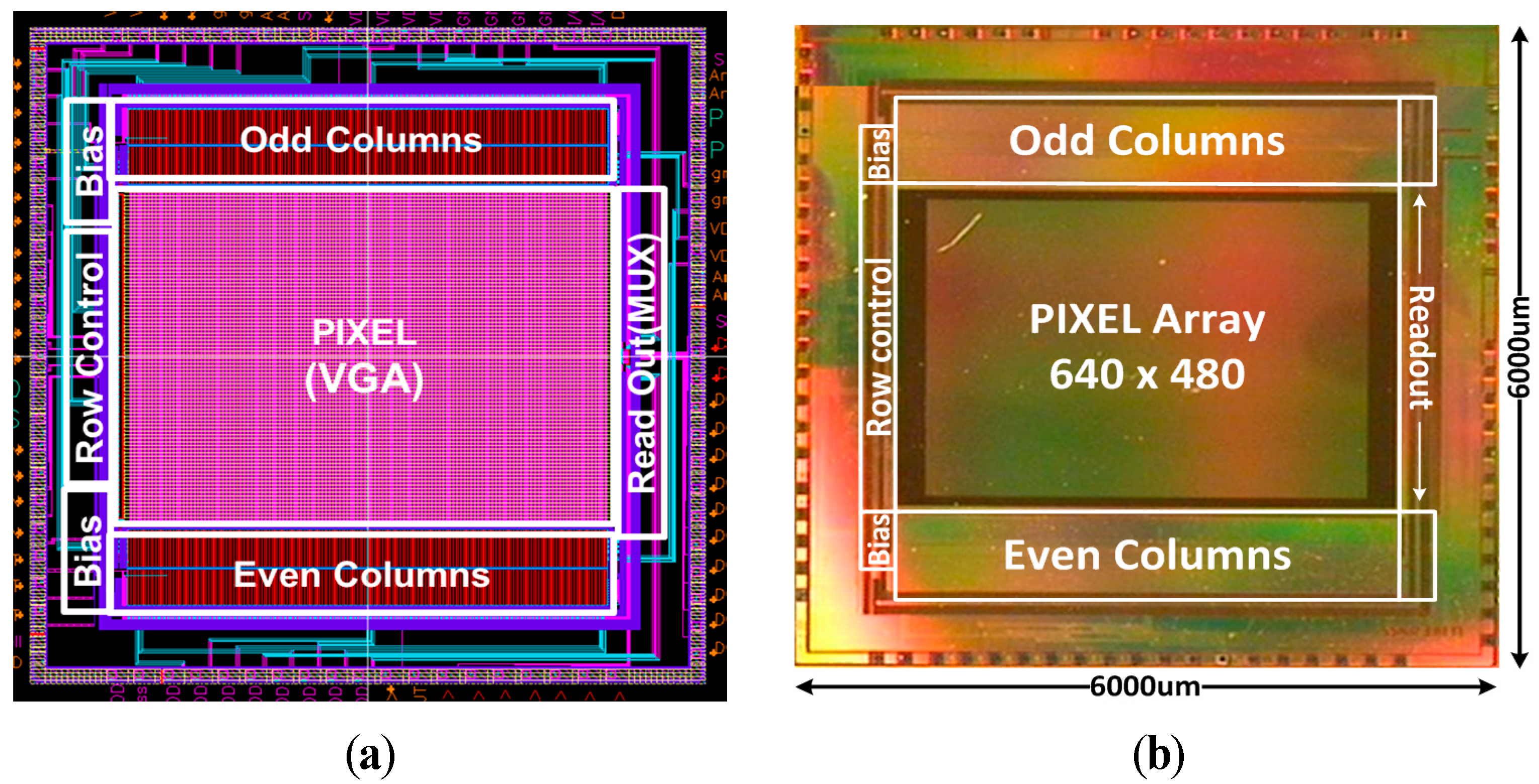
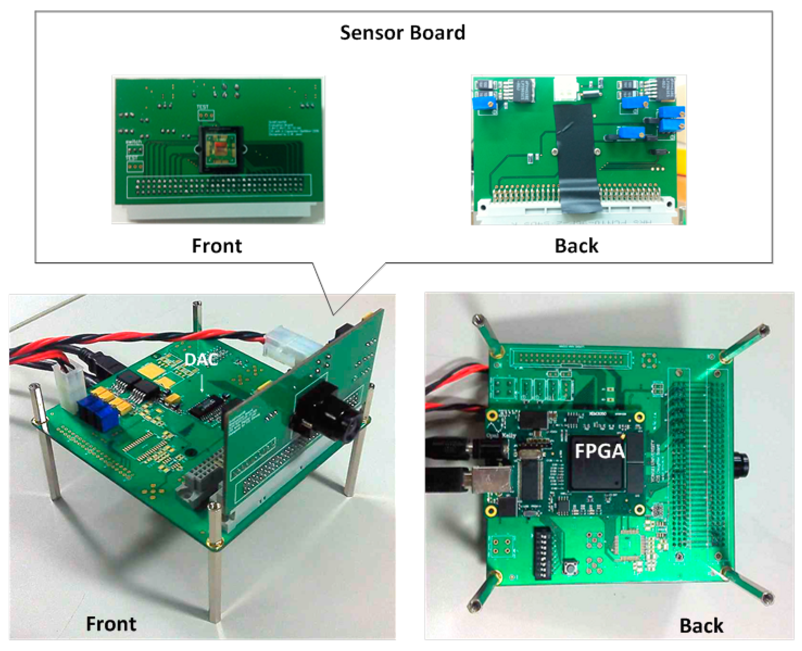
4. Experimental Results


5. Conclusions
| Process Technology | 0.13 um 1P4M CIS Process |
|---|---|
| Chip size | 6 mm × 6 mm |
| Core size | 5 mm × 5 mm |
| Number of pixel | 640 × 480 pixels |
| Pixel type | Non-shared 4T (pinned-photodiode) |
| Operating voltage | 2.8 V (pixel)/2.8 V (analog)/1.5 (digital) |
| Frame rate | 131 fps (@100 M Hz) |
| ADC resolution | 10-bit |
| Pixel FPN | 0.48 LSB (@ dark) |
| Column FPN | 0.45 LSB (@ dark) |
| Random Noise | 0.35 LSB (@ dark) |
| Dynamic range | 84 dB |
| Power consumption | 54 µW/column |
| Full well capacity | 23,000 |
| Conversion gain | 43 µV/ |
| Figure of Merit | 41. 4 nJ |
| Reference | [15] | [16] | [17] | [18] | This Work |
|---|---|---|---|---|---|
| Technology | 0.13 um CIS | 0.18 um CIS | 0.13 um CIS | 0.18 um CIS | 0.13 um CIS |
| CDS Type | Analog CDS | Digital CDS | Digital CDS | Analog CDS | Digital CDS |
| ADC Type | Single-slope | Single-slope | Single-slope | TS Cyclic | Single-slope |
| ADC resolution | 11-bit | 10-bit, 12-bit (configurable) | 12-bit, 14-bit (configurable) | 12-bit | 10-bit |
| Pixel size (um) | 2.25 × 2.25 | 3.63 × 3.63 | 4.2 × 4.2 | 2.8 × 2.8 | 5.6 × 5.6 |
| Pixel Array | 640 × 480 | 1920 × 1440 | 8192 × 2160 | 7680 × 4320 | 640 × 480 |
| Frame Rate (fps) | 30 | 180 (10-bit) | 120 (12-bit) | 120 | 131 |
| Power (mW) | 44.1 | 580 | 3000 (120 fps) | 2500 | 39.2 |
Acknowledgments
Author Contributions
Conflicts of Interest
References
- Sugiki, T.; Ohsawa, S.; Miura, H.; Sasaki, M.; Nakamura, N.; Inoue, I.; Hoshino, M.; Tomizawa, Y.; Arakawa, T. A 60 mW 10 b CMOS image sensor with column-to-column FPN reduction. In Proceedings of the IEEE Solid-State Circuit Conference Digest Of Technical Papers (ISSCC), San Francisco, CA, USA, 9 February 2000; pp. 108–109.
- Lim, S.; Cheon, J.; Ham, S.; Han, G. A new correlated double sampling and single slope ADC circuit for CMOS image sensors. In Proceedings of the International SoC Design Conference (ISOCC), Seoul, Korea, 26–27 October 2004; pp. 239–241.
- Snoeij, F.; Theuwissen, A.; Makinwa, K.A.; Huijsing, J. Multiple-ramp column-parallel ADC architectures for CMOS image sensors. IEEE J. Solid-State Circuits 2007, 42, 2968–2967. [Google Scholar] [CrossRef]
- Snoeij, F.; Theuwissen, A.; Makinwa, K.A.; Huijsing, J. A CMOS imager with column-level ADC using dynamic column fixed-pattern noise reduction. IEEE J. Solid-State Circuits 2006, 41, 3007–3015. [Google Scholar] [CrossRef]
- Lee, D.; Han, G. High-speed, low-power correlated double sampling counter for column-parallel CMOS imagers. Electron. Lett. 2007, 43, 1362–1364. [Google Scholar] [CrossRef]
- Yamada, T.; Kasuga, S.; Murata, T.; Kato, Y. A 140dB-dynamic-range MOS image sensor with in-pixel multiple-exposure synthesis. In Proceedings of the IEEE International Solid-State Circuits Conference Digest of Technical Papers (ISSCC), San Francisco, CA, USA, 3–7 February 2008; pp. 593–594.
- Ham, S.H.; Lee, Y.H.; Jung, W.K.; Lim, S.H.; Yoo, K.C.; Chae, Y.C.; Cho, J.H.; Lee, D.M.; Han, G.H. CMOS image sensor with analog gamma correction using nonlinear single-slope ADC. In Proceedings of the IEEE International Symposium on Circuits and Systems (ISCAS), Island of Kos, Greece, 21–24 May 2006; pp. 3578–3581.
- Takayanagi, I.; Shirakawa, M.; Mitani, K.; Sugawara, M.; Iversen, S.; Moholt, J.; Nakamura, J.; Fossum, E. A 1.25-inch 60-frames/s 8.3-M-pixel digital-output CMOS image sensor. IEEE J. Solid-State Circuits 2005, 40, 2305–2314. [Google Scholar] [CrossRef]
- Yoshihara, S.; Kikuchi, M.; Ito, Y.; Inada, Y.; Kuramochi, S.; Wakabayashi, H.; Okano, M.; Koseki, K.; Kuriyama, H.; Inutsuka, J.; et al. A 1/1.8-inch 6.4Mpixel 60 frames/s CMOS image sensor with seamless mode change. IEEE J. Solid-State Circuits 2006, 41, 2998–3006. [Google Scholar] [CrossRef]
- Cheon, J.; Han, G. Noise analysis and simulation method for a single-slope ADC with CDS in a CMOS image sensor. IEEE Trans. Circuits Syst. I 2008, 55, 2980–2987. [Google Scholar] [CrossRef]
- Krymski, A.; Bock, N.; Tu, N.; Blerkom, D.; Fossum, E. A high-speed, 240-frames/s, 4.1-Mpixel CMOS sensor. IEEE Trans. Electron Devices 2003, 50, 130–135. [Google Scholar] [CrossRef]
- Yang, W.; Kwon, O.; Lee, J.; Hwang, G.; Lee, S. An integrated 800 × 600 CMOS imaging system. In Proceedings of the IEEE Solid-State Circuit Conference Digest of Technical Papers (ISSCC), San Francisco, CA, USA, 17 February 1999; pp. 304–305.
- Chae, Y.-C.; Cheon, J.-M.; Lim, S.-H.; Kwon, M.-H.; Yoo, K.-S.; Jung, W.-K.; Lee, D.-H.; Ham, S.-H.; Han, G.-H. A 2.1 M pixels, 120 frame/s CMOS image sensor with column-parallel ΔΣ architecture. IEEE J. Solid-State Circuits 2011, 46, 236–247. [Google Scholar] [CrossRef]
- Bae, J.; Kim, D.; Ham, S.; Chae, Y.; Song, M. A two-step A/D conversion and column self-calibration technique for low noise CMOS image sensors. Sensors 2014, 14, 11825–11843. [Google Scholar] [CrossRef] [PubMed]
- Cho, N.; Song, B.; Kim, K.; Burm, J.; Han, S. A VGA CMOS image sensor with 11-bit column parallel single-slope ADCs. In Proceedings of the International SoC Design Conference (ISOCC), Seoul, Korea, 22–23 November 2010; pp. 25–27.
- Nitta, Y.; Muramatsu, Y.; Amano, K.; Toyama, T.; Yamamoto, J.; Mishina, K.; Suzuki, A.; Taura, T.; Kato, A.; Kikuchi, M. High-speed digital double sampling with analog CDS on column parallel ADC architecture for low-noise active pixel sensor. In Proceedings of the IEEE International Solid-State Circuits Conference Digest of Technical Papers (ISSCC), San Francisco, CA, USA, 6–9 February 2006; pp. 2024–2031.
- Toyama, T.; Mishina, K.; Tsuchiya, H.; Ichikawa, T.; Iwaki, H.; Gendai, Y.; Murakami, H.; Takamiya, K.; Shiroshita, H.; Muramatsu, Y.; et al. A 17.7 M pixel 120 fps CMOS image sensor with 34.8 Gb/s readout. In Proceedings of the IEEE International Solid-State Circuits Conference Digest of Technical Papers (ISSCC), San Francisco, CA, USA, 20–24 February 2011; pp. 420–422.
- Watabe, T.; Kitamura, K.; Sawamoto, T.; Kosugi, T.; Akahori, T.; Iida, T.; Isobe, K.; Watanabe, T.; Shimamoto, H.; Ohtake, H.; et al. A 33 M pixel 120 fps CMOS image sensor for UDTV application with two-stage column-parallel cyclic ADCs. In Proceedings of the IEEE International Solid-State Circuits Conference Digest of Technical Papers (ISSCC), San Francisco, CA, USA, 19–23 February 2012; pp. 388–390.
- Cho, K.; Kim, D.; Song, M. A low power dual CDS for a column-parallel CMOS image sensor. J. Semicond. Technol. Sci. 2012, 12, 388–396. [Google Scholar] [CrossRef]
© 2015 by the authors; licensee MDPI, Basel, Switzerland. This article is an open access article distributed under the terms and conditions of the Creative Commons Attribution license (http://creativecommons.org/licenses/by/4.0/).
Share and Cite
Kim, D.; Bae, J.; Song, M. A High Speed CMOS Image Sensor with a Novel Digital Correlated Double Sampling and a Differential Difference Amplifier. Sensors 2015, 15, 5081-5095. https://doi.org/10.3390/s150305081
Kim D, Bae J, Song M. A High Speed CMOS Image Sensor with a Novel Digital Correlated Double Sampling and a Differential Difference Amplifier. Sensors. 2015; 15(3):5081-5095. https://doi.org/10.3390/s150305081
Chicago/Turabian StyleKim, Daehyeok, Jaeyoung Bae, and Minkyu Song. 2015. "A High Speed CMOS Image Sensor with a Novel Digital Correlated Double Sampling and a Differential Difference Amplifier" Sensors 15, no. 3: 5081-5095. https://doi.org/10.3390/s150305081
APA StyleKim, D., Bae, J., & Song, M. (2015). A High Speed CMOS Image Sensor with a Novel Digital Correlated Double Sampling and a Differential Difference Amplifier. Sensors, 15(3), 5081-5095. https://doi.org/10.3390/s150305081