Inorganic Boron-Based Nanostructures: Synthesis, Optoelectronic Properties, and Prospective Applications


Abstract
:1. Introduction
2. Synthesis Methods of Inorganic Boron-Based Nanostructures
2.1. One-Dimensional Boron-Based Nanomaterials
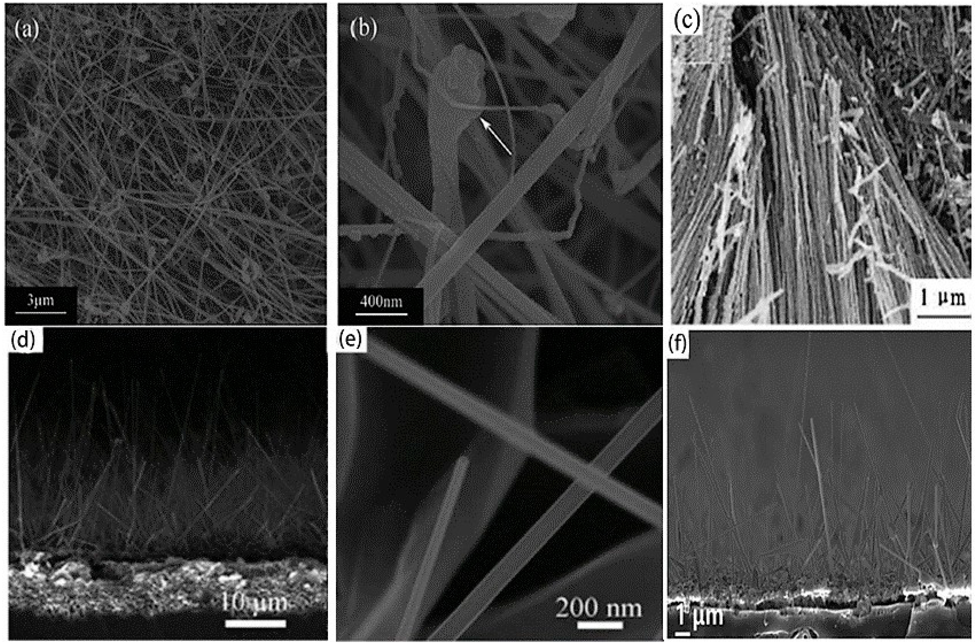
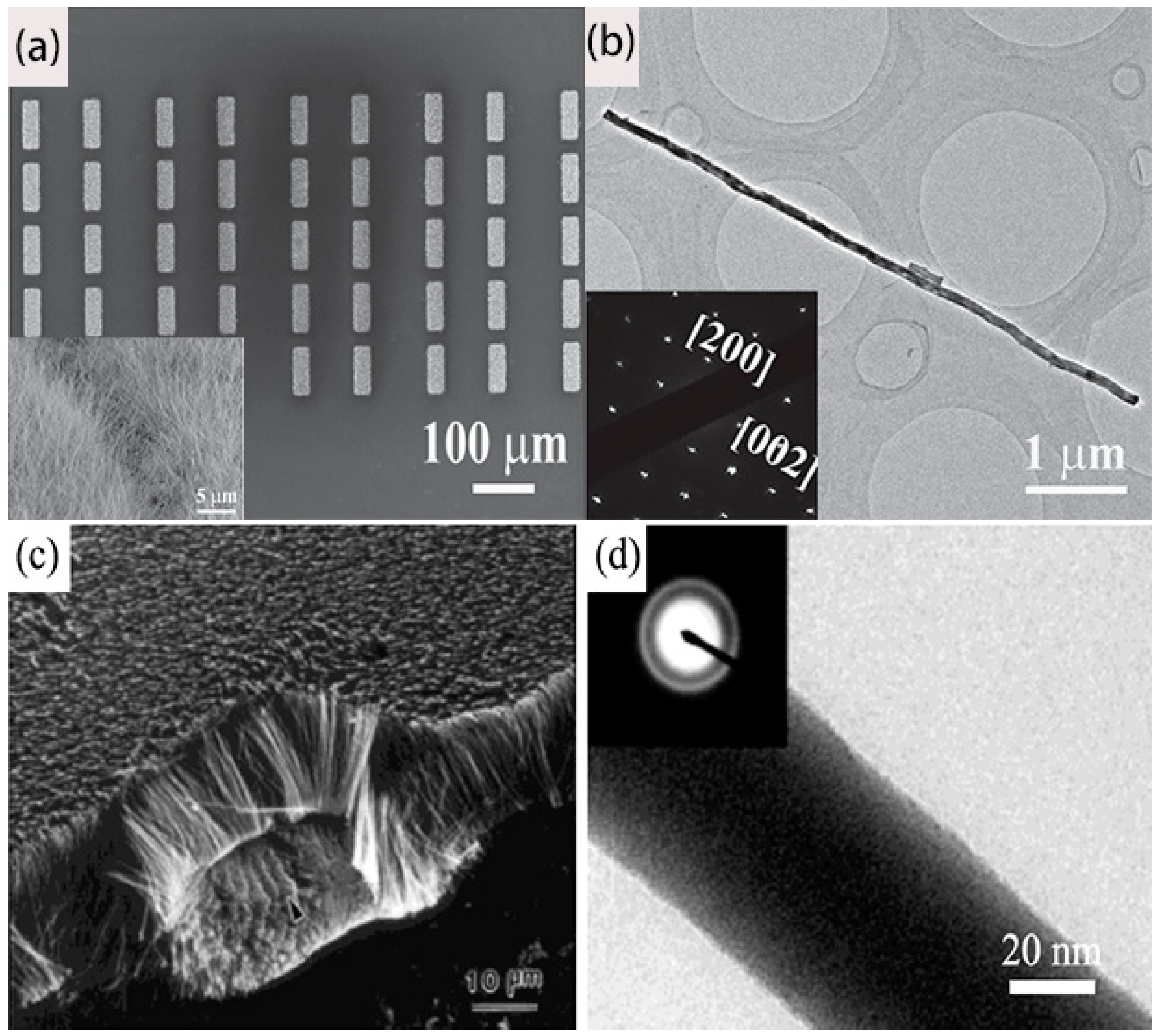
2.1.1. Rare-Earth Boride Nanostructures
2.1.2. Boron Single Element Nanostructures
Boron Nanowires
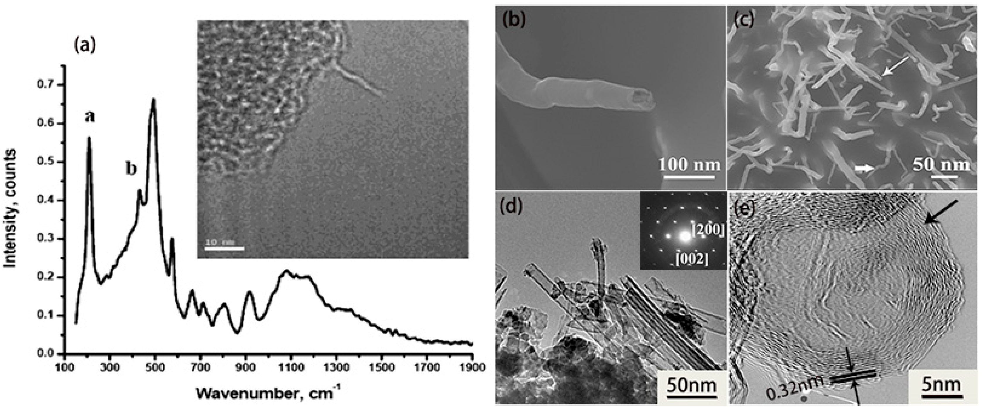
Boron Nanotube
2.2. Two-Dimensional Boron-Based Nanomaterials
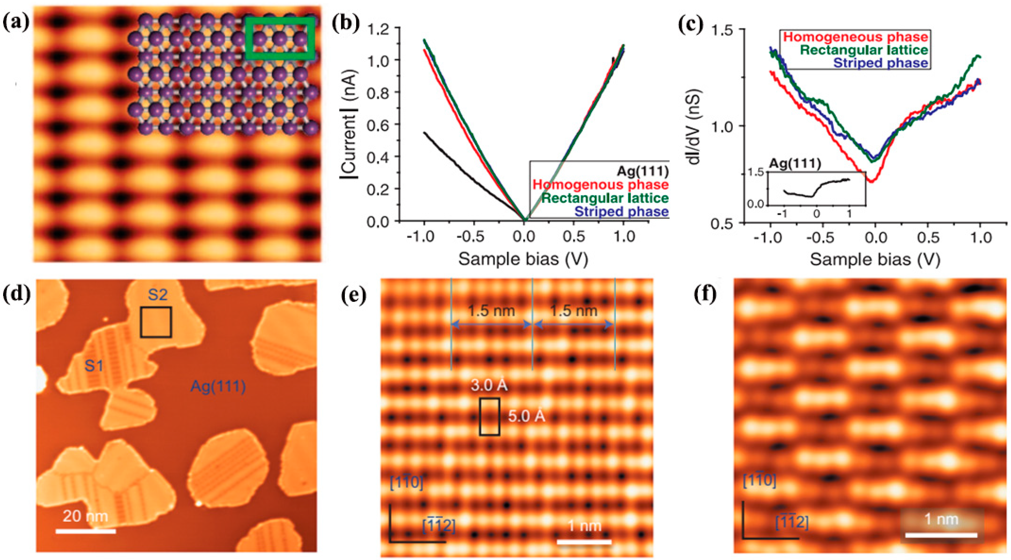
2.2.1. Two-Dimensional Boron Monoelement Nanostructures
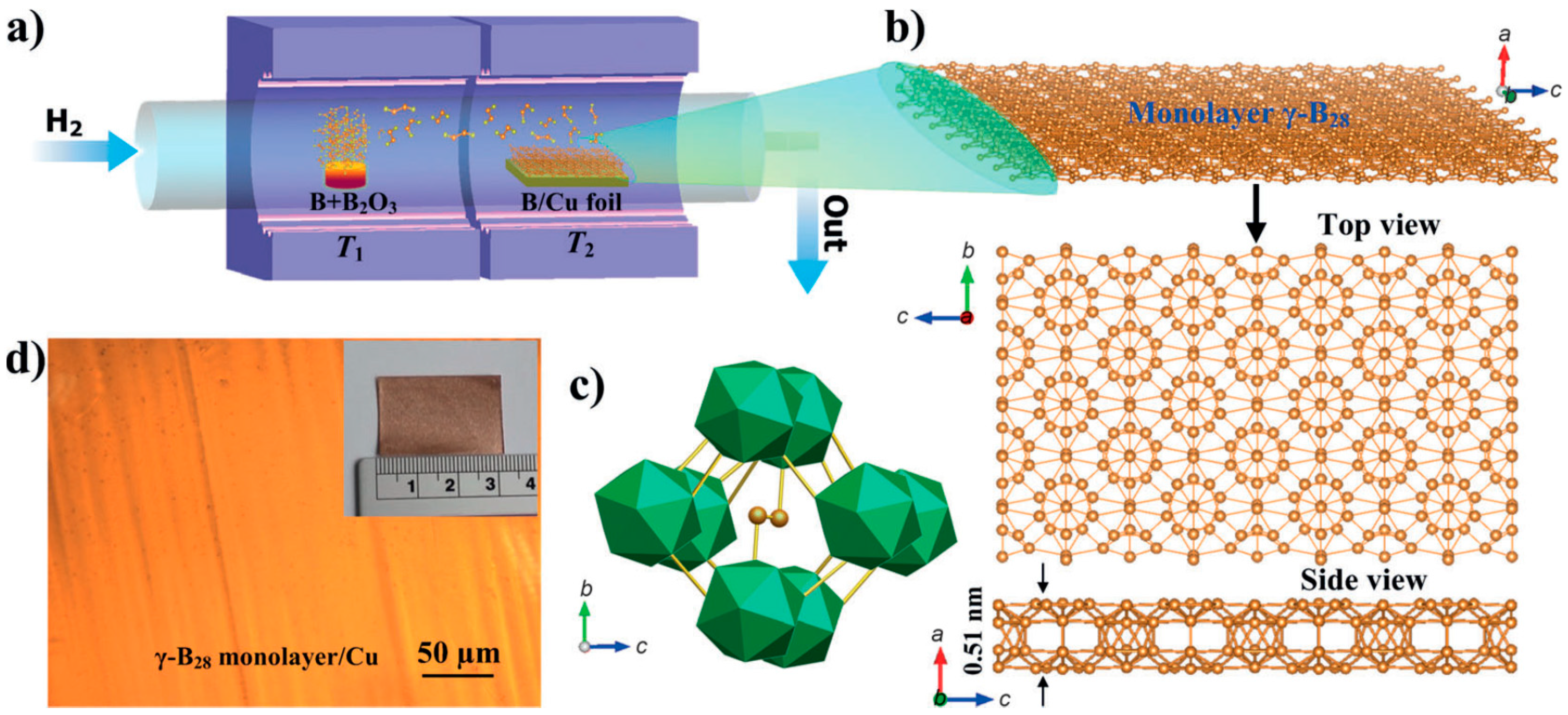
2.2.2. Two-Dimensional Boron-Based Nanostructures
3. Optoelectronic Properties
3.1. Electrical Properties
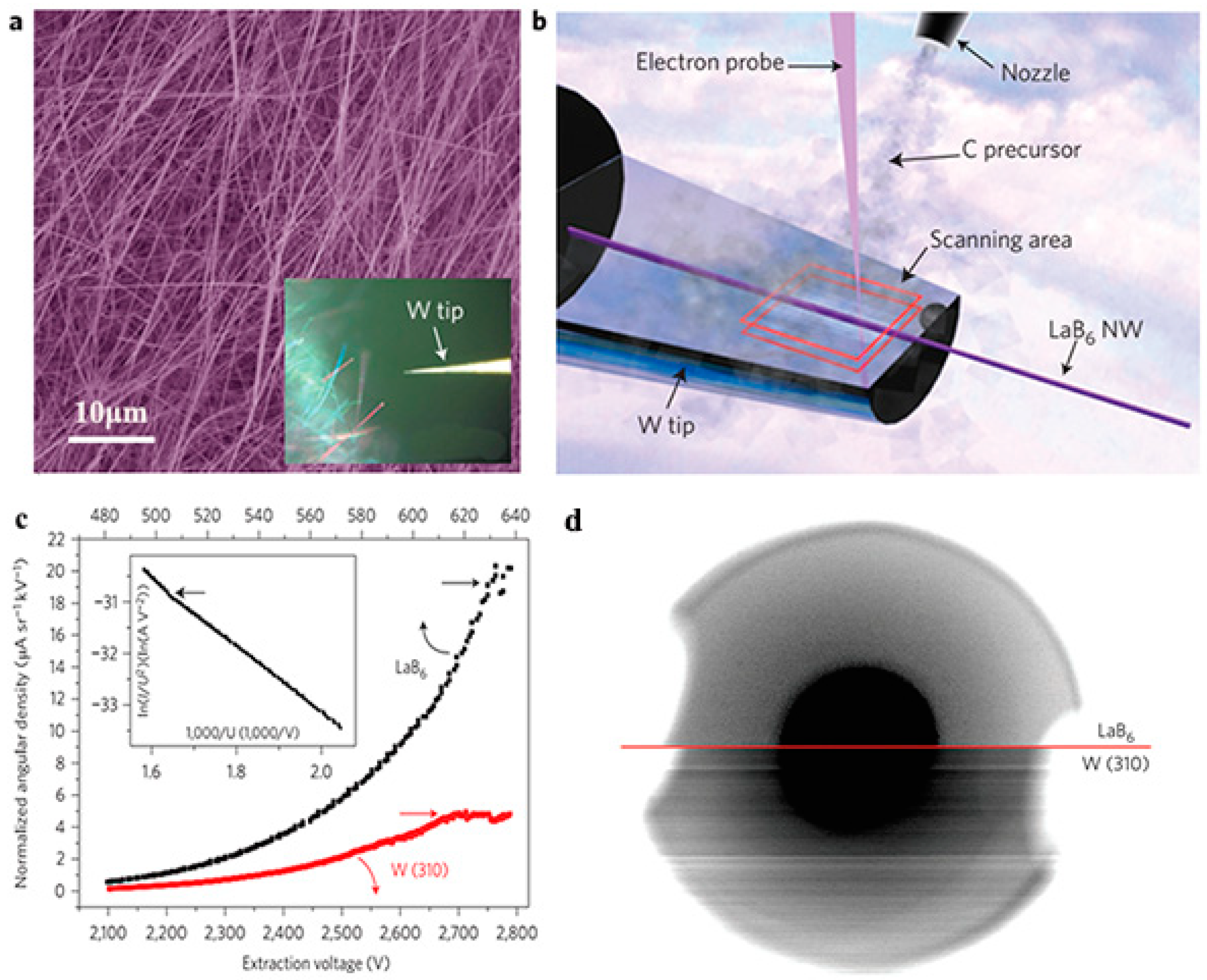
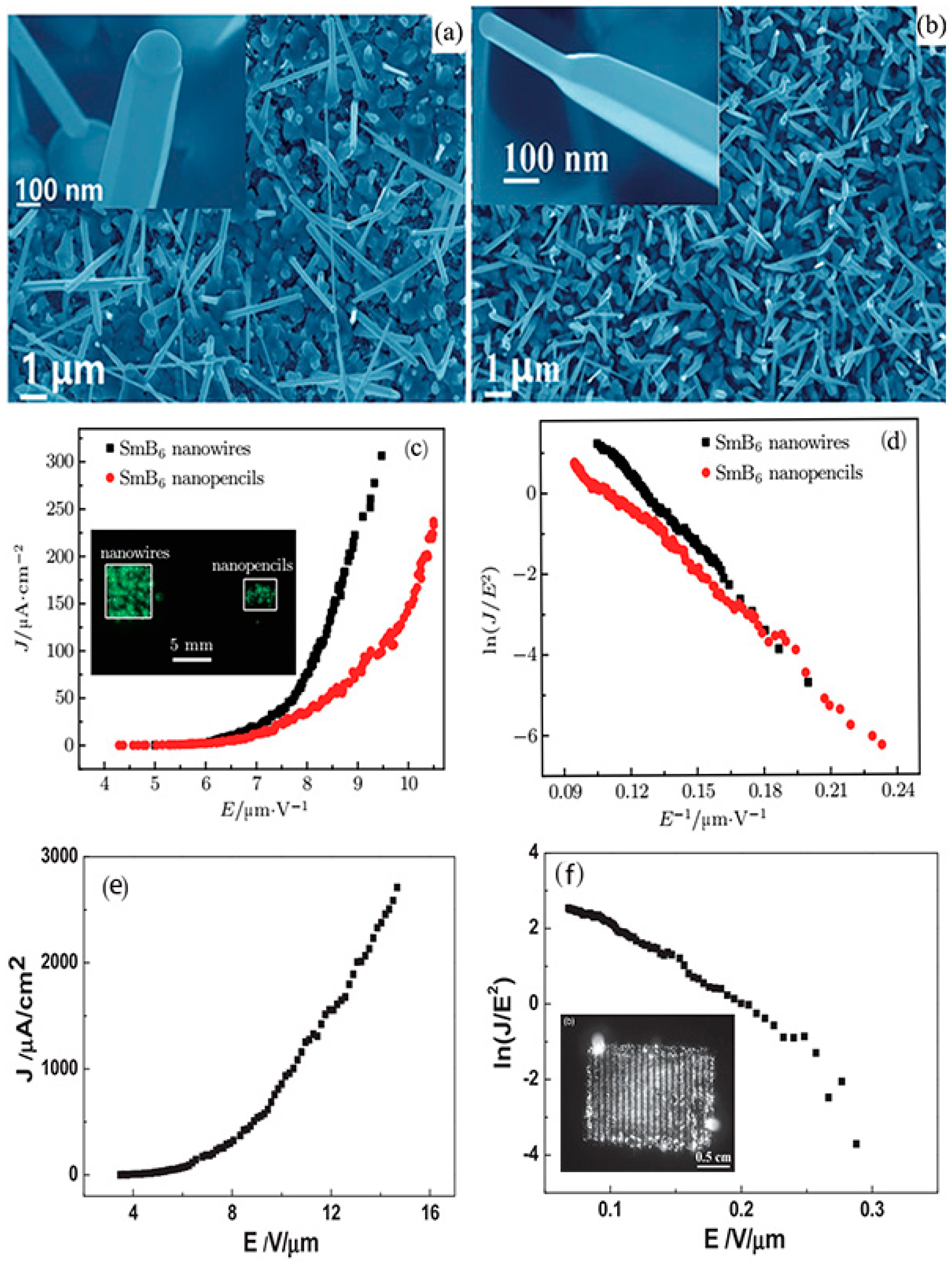
3.1.1. Field Emission (FE) Properties
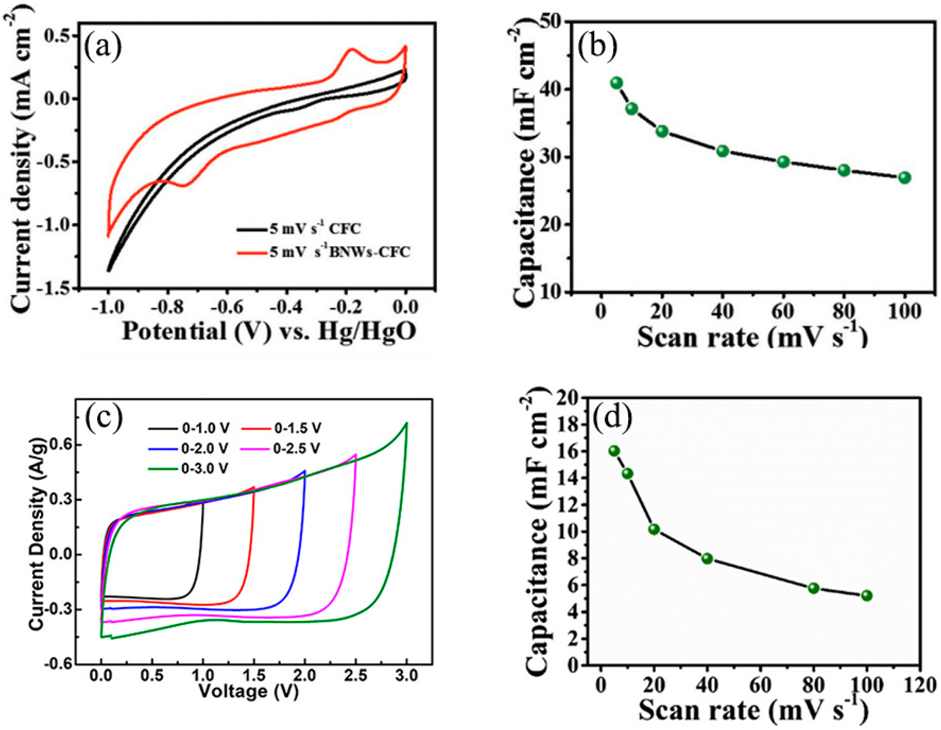
3.1.2. Capacitance Characteristics
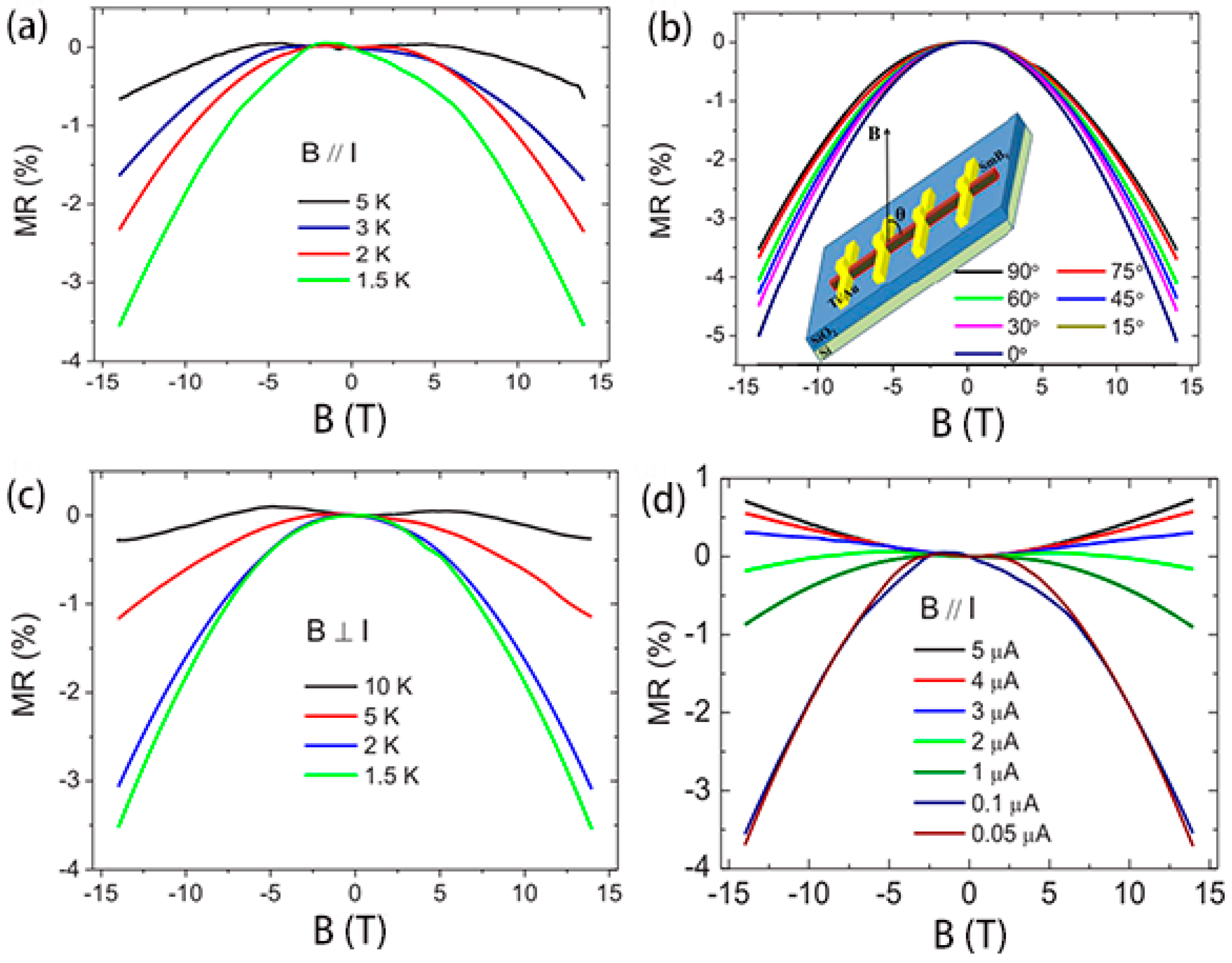
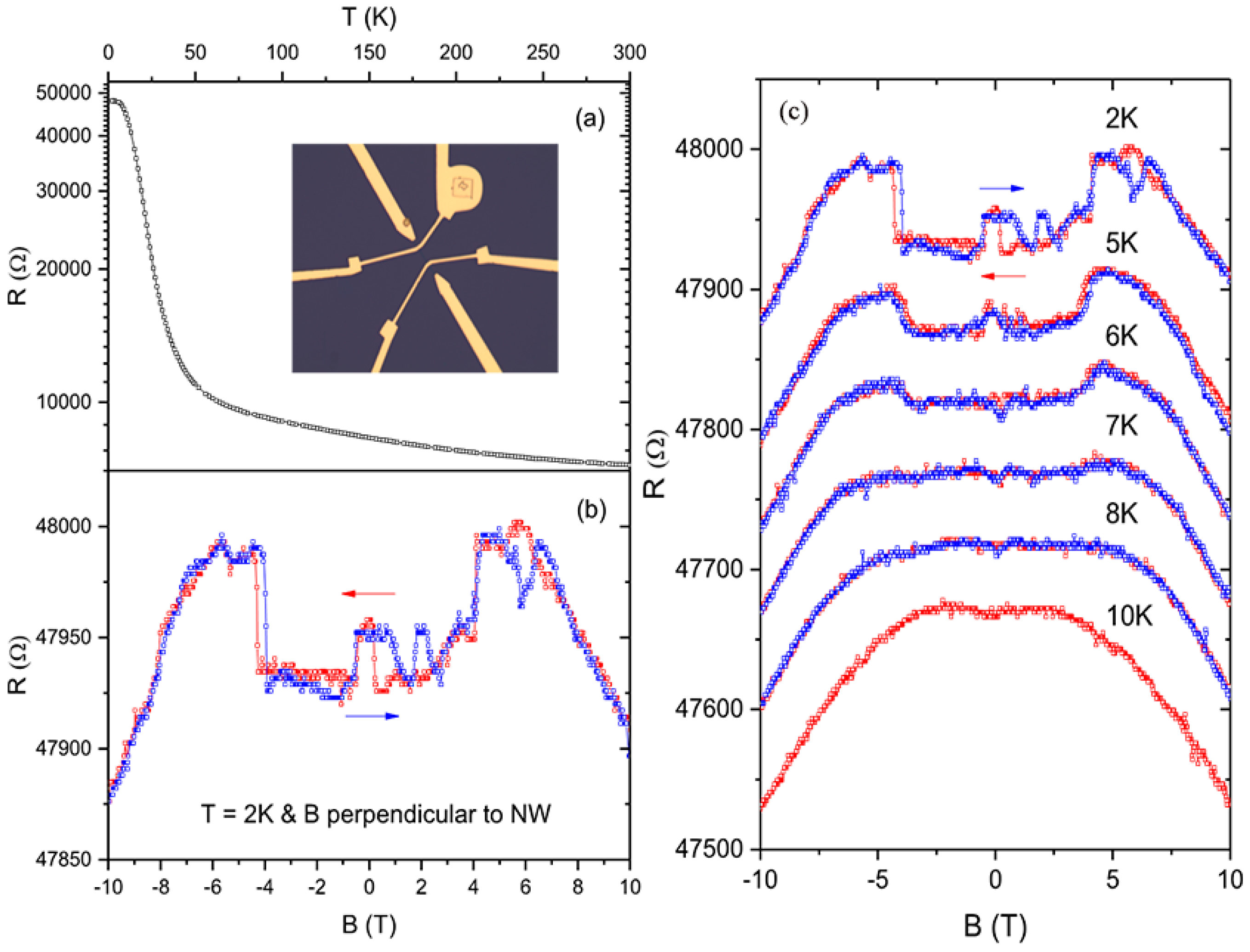
3.1.3. Surface Electrical Transport Property
3.2. Optical Properties
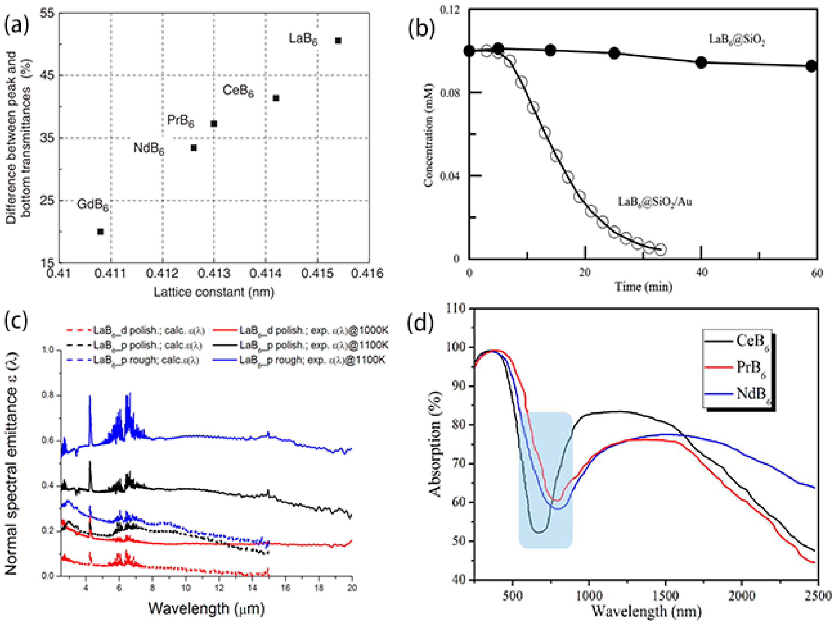
3.2.1. Optical Absorption
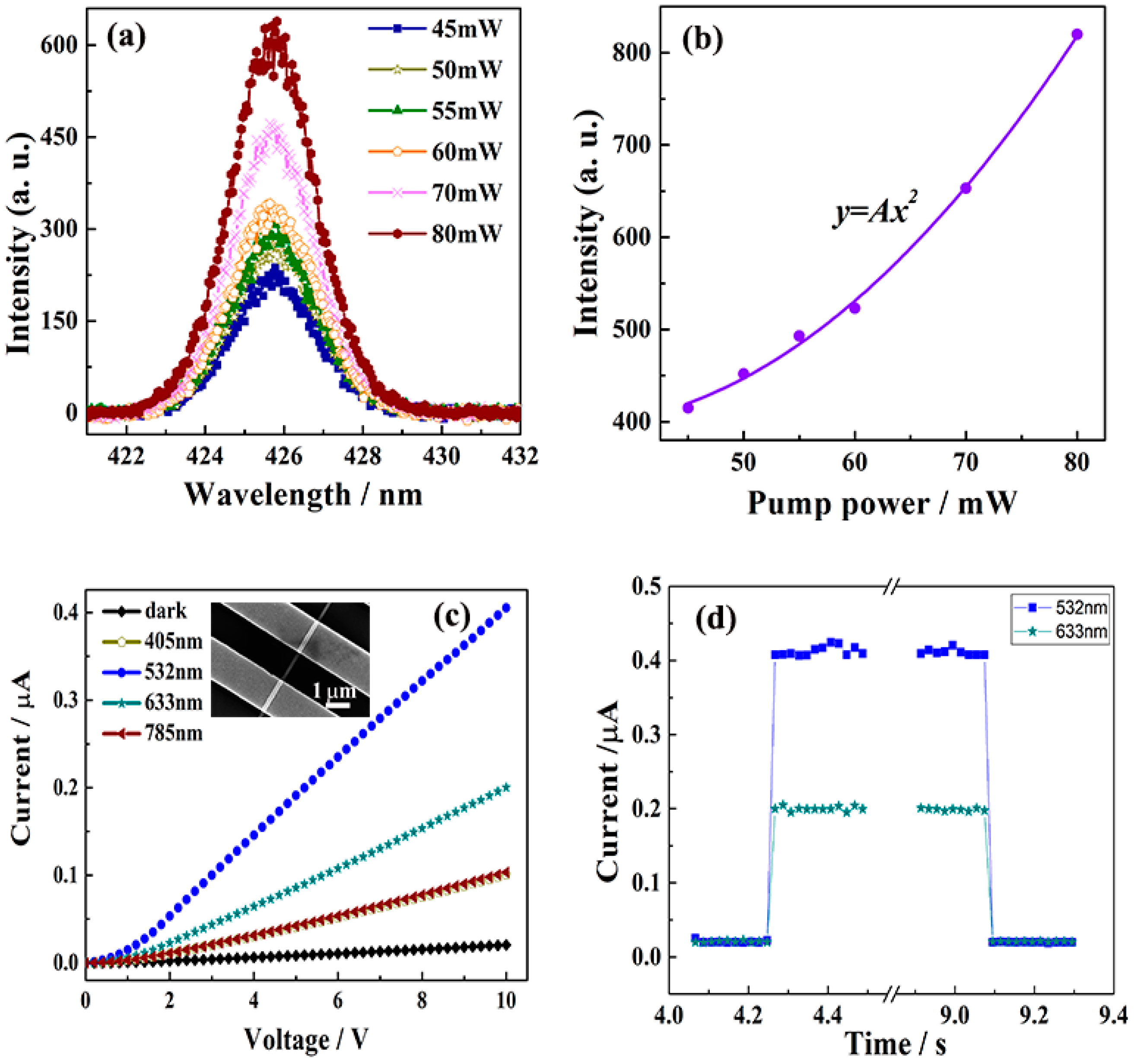
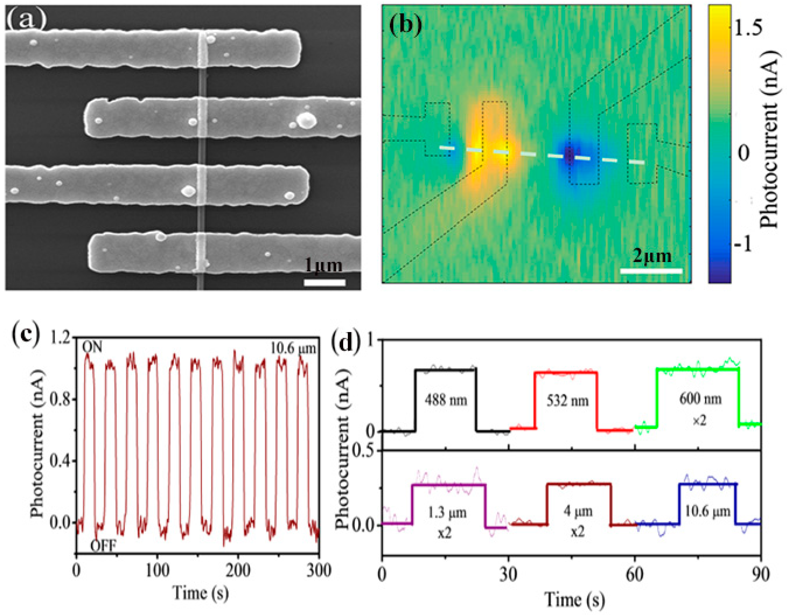
3.2.2. Photosensitive Properties
4. Outlook and Conclusions
Author Contributions
Funding
Conflicts of Interest
References
- Tsagareishvili, G.V.; Tavadze, F.N. Boron crystals: Preparation, structure and properties. Prog. Cryst. Growth Charact. 1988, 16, 341–365. [Google Scholar] [CrossRef]
- Emin, D. Icosahedral boron-rich solids. Phys. Today 1987, 40, 55–62. [Google Scholar] [CrossRef]
- Gaule, G.K. Boron: Preparation, Properties, and Application; Plenum: New York, NY, USA, 1965. [Google Scholar]
- Ulas, A.; Kuo, K.K.; Gotzmer, C. Ignition and combustion of boron particles in fluorine-containing environments. Combust. Flame 2001, 127, 1935–1957. [Google Scholar] [CrossRef]
- Davis, P.R.; Gesley, M.A.; Schwind, G.A.; Swanson, L.W.; Hutta, J.J. Comparison of thermionic cathode parameters of low index single crystal faces of LaB6, CeB6 and PrB6. Appl. Surf. Sci. 1989, 37, 381–394. [Google Scholar] [CrossRef]
- Otani, S.; Ishizawa, Y. Thermionic emission properties of boron-rich LaB6 and CeB6 crystal cathodes. J. Alloys Compd. 1996, 1, L18–L20. [Google Scholar] [CrossRef]
- Sträter, N. William Nunn Lipscomb, Jr. (1919–2011). Angew. Chem. 2011, 123, 7874–7875. [Google Scholar]
- Cui, Y.; Lieber, C.M. Functional nanoscale electronic devices assembled using silicon nanowire building blocks. Science 2001, 291, 851–853. [Google Scholar] [CrossRef]
- Osada, M.; Sasaki, T. Two-dimensional dielectric nanosheets: Novel nanoelectronics from nanocrystal building blocks. Adv. Mater. 2012, 24, 210–228. [Google Scholar] [CrossRef]
- Chen, C.H.; Aizawa, T.; Iyi, N.; Sato, A.; Otani, S. Structural refinement and thermal expansion of hexaborides. J. Alloys Compd. 2004, 366, L6–L8. [Google Scholar] [CrossRef]
- Kimura, S.; Nanba, T.; Tomikawa, M.; Kunii, S.; Kasuya, T. Electronic structure of rare-earth hexaborides. Phys. Rev. B 1992, 46, 12196–12204. [Google Scholar] [CrossRef]
- Peysson, Y.; Ayache, C.; Salce, B.; Rossat-Mignod, J.; Kunii, S.; Kasuya, T. Thermal properties of CeB6 and LaB6. J. Magn. Magn. Mater. 1985, 47, 63–65. [Google Scholar] [CrossRef]
- Zhang, H.; Tang, J.; Yuan, J.S.; Ma, J.; Shinya, N.; Nakajima, K.; Murakami, H.; Ohkubo, T.; Qin, L.C. Nanostructured LaB6 field emitter with lowest apical work function. Nano Lett. 2010, 10, 3539–3544. [Google Scholar] [CrossRef]
- Zhang, H.; Zhang, Q.; Tang, J.; Qin, L.C. Single-crystalline LaB6 nanowires. J. Am. Chem. Soc. 2005, 127, 2862–2863. [Google Scholar] [CrossRef]
- Ordanyan, S.S.; Vikhman, S.V.; Nesmelov, D.D.; Danilovich, D.P.; Panteleev, I.B. Nonoxide high-melting point compounds as materials for extreme conditions. Adv. Sci. Tech. 2014, 89, 47–56. [Google Scholar] [CrossRef]
- Zhang, H.; Tang, J.; Zhang, L.; An, B.; Qin, L.C. Atomic force microscopy measurement of the Young’s modulus and hardness of single LaB6 nanowires. Appl. Phys. Lett. 2008, 92, 173121. [Google Scholar] [CrossRef]
- Moore, J.E. The birth of topological insulators. Nature 2010, 464, 194–198. [Google Scholar] [CrossRef]
- Dzero, M.; Sun, K.; Galitski, V.; Coleman, P. Topological Kondo insulators. Phys. Rev. Lett. 2010, 104, 2909–2915. [Google Scholar] [CrossRef]
- Jiang, J.; Li, S.; Zhang, T.; Sun, Z.; Chen, F.; Ye, Z.R.; Xu, M.; Ge, Q.Q.; Tan, S.Y.; Niu, X.H.; et al. Observation of possible topological in-gap surface states in the Kondo insulator SmB6 by photoemission. Nat. Commun. 2013, 4, 3010. [Google Scholar] [CrossRef]
- Li, G.; Xiang, Z.; Yu, F.; Asaba, T.; Lawson, B.; Cai, P.; Tinsman, C.; Berkley, A. Two-dimensional Fermi surfaces in Kondo insulator SmB6. Science 2014, 346, 1208–1212. [Google Scholar] [CrossRef]
- Kim, D.J.; Xia, J.; Fisk, Z. Topological surface state in the Kondo insulator samarium hexaboride. Nat. Mater. 2014, 13, 466–470. [Google Scholar] [CrossRef] [Green Version]
- He, X.S.; Gan, H.B.; Du, Z.Z.; Ye, B.C.; Zhou, L.; Tian, Y.; Deng, S.Z.; Guo, G.P.; Lu, H.Z.; Liu, F.; He, H.T. Magnetoresistance anomaly in topological Kondo insulator SmB6 nanowires with strong surface magnetism. Adv. Sci. 2018, 5, 1700753. [Google Scholar] [CrossRef]
- Tai, G.; Hu, T.S.; Zhou, Y.G.; Wang, X.F.; Kong, J.Z.; Zeng, T.; You, Y.C.; Wang, Q. Synthesis of atomically thin boron films on copper foils. Angew. Chem. Int. Ed. 2015, 127, 15693–15697. [Google Scholar] [CrossRef]
- Mannix, A.J.; Zhou, X.F.; Kiraly, B.; Wood, D.; Alducin, D.; Myers, B.D.; Liu, X.L.; Fisher, B.L.; Santiago, U.; Guest, J.R.; et al. Synthesis of borophenes: Anisotropic, two-dimensional boron polymorphs. Science 2015, 350, 1513–1516. [Google Scholar] [CrossRef] [PubMed] [Green Version]
- Feng, B.J.; Zhang, J.; Zhong, Q.; Li, W.B.; Li, S.; Li, H.; Cheng, P.; Meng, S.; Chen, L.; Wu, K.H. Experimental realization of two-dimensional boron sheets. Nat. Chem. 2016, 8, 563–568. [Google Scholar] [CrossRef] [Green Version]
- Jiang, H.R.; Lu, Z.; Wu, M.C.; Ciucci, F.; Zhao, T.S. Borophene: A promising anode material offering high specific capacity and high rate capability for lithium-ion batteries. Nano Energy 2016, 23, 97–104. [Google Scholar] [CrossRef]
- Li, W.L.; Chen, Q.; Tian, W.J.; Bai, H.; Zhao, Y.F.; Hu, H.S.; Li, J.; Zhai, H.J.; Li, S.D.; Wang, L.S. The B35 cluster with a double-hexagonal vacancy: A new and more flexible structural motif for borophene. J. Am. Chem. Soc. 2014, 136, 12257–12260. [Google Scholar] [CrossRef]
- Zhang, X.M.; Hu, J.; Cheng, Y.; Yang, H.Y.; Yao, Y.; Yang, S.A. Borophene as an extremely high capacity electrode material for Li-ion and Na-ion batteries. Nanoscale 2016, 8, 15340–15347. [Google Scholar] [CrossRef] [Green Version]
- Xia, Y.; Yang, P.; Sun, Y.; Wu, Y.; Mayers, B.; Gates, B.; Yin, Y.; Kim, F.; Yan, H. One-dimensional nanostructures: Synthesis, characterization, and applications. Adv. Mater. 2003, 15, 353–389. [Google Scholar] [CrossRef]
- Kauffman, D.R.; Star, A. Single-walled carbon-nanotube spectroscopic and electronic field-effect transistor measurements: A combined approach. Small 2007, 3, 1324–1329. [Google Scholar] [CrossRef]
- Li, H.; Wang, X.; Xu, J.; Zhang, Q.; Bando, Y.; Golberg, D.; Ma, Y.; Zhai, T.Y. One-Dimensional CdS Nanostructures: A promising candidate for optoelectronics. Adv. Mater. 2013, 25, 3017–3037. [Google Scholar] [CrossRef] [PubMed]
- Wang, Z.X.; Safdar, M.; Jiang, C.; He, J. High-performance UV–Visible–NIR broad spectral photodetectors based on one-dimensional In2Te3 nanostructures. Nano Lett. 2012, 12, 4715–4721. [Google Scholar] [CrossRef]
- Ahn, S.H.; Kim, D.J.; Chi, W.S.; Kim, J.H. One-dimensional hierarchical nanostructures of TiO2 nanosheets on SnO2 Nanotubes for high efficiency solid-state dye-sensitized solar Cells. Adv. Mater. 2013, 25, 4893–4897. [Google Scholar] [CrossRef]
- Xu, J.Q.; Hou, G.H.; Li, H.Q.; Zhai, T.Y.; Dong, B.P.; Yan, H.L.; Wang, Y.R.; Yu, B.H.; Bando, Y.; Golberg, D. Fabrication of vertically aligned single-crystalline lanthanum hexaboride nanowire arrays and investigation of their field emission. NPG Asia Mater. 2013, 5, e53. [Google Scholar] [CrossRef]
- Zou, X.M.; Wang, J.L.; Liu, X.Q.; Wang, C.L.; Jiang, Y.; Wang, Y.; Xiao, X.H.; Ho, J.C.; Li, J.C.; Jiang, C.Z.; et al. Rational design of sub-parts per million specific gas sensors array based on metal nanoparticles decorated nanowire enhancement-mode transistors. Nano Lett. 2013, 13, 3287–3292. [Google Scholar] [CrossRef]
- Zhao, X.; Cai, B.; Tang, Q.; Tong, Y.; Liu, Y. One-dimensional nanostructure field-effect sensors for gas detection. Sensors 2014, 14, 13999–14020. [Google Scholar] [CrossRef]
- Tian, J.; Xu, Z.C.; Shen, C.M.; Liu, F.; Xu, N.S.; Gao, H.J. One-dimensional boron nanostructures: Prediction, synthesis, characterizations, and applications. Nanoscale 2010, 2, 1375–1389. [Google Scholar] [CrossRef]
- Chi, M.; Zhao, Y.; Fan, Q.; Han, W. The synthesis of PrB6 nanowires and nanotubes by the self-catalyzed method. Ceram. Int. 2014, 40, 8921–8924. [Google Scholar] [CrossRef]
- Han, W.; Qiu, Y.; Zhao, Y.M.; Zhang, H.; Chen, J.; Sun, S.; Lan, L.F.; Fan, Q.H.; Li, Q.D. Low-temperature synthesis and electronic transport of topological insulator SmB6 nanowires. CrystEngComm. 2016, 18, 7934. [Google Scholar] [CrossRef]
- Fan, Q.; Zhang, Q.; Zhao, Y.; Ding, Q.W. Field emission from one-dimensional single-crystalline NdB6 nanowires. J. Rare Earths. 2013, 31, 145–148. [Google Scholar] [CrossRef]
- Ji, X.H.; Zhang, Q.Y.; Xu, J.Q.; Zhao, Y.M. Rare-earth hexaborides nanostructures: Recent advances in materials, characterization and investigations of physical properties. Prog. Solid State Chem. 2011, 39, 51–69. [Google Scholar] [CrossRef]
- Zhang, H.; Zhang, Q.; Zhao, G.; Tang, J.; Zhou, O.; Qin, L.C. Single-crystalline GdB6 nanowire field emitters. J. Am. Chem. Soc. 2005, 127, 13120–13121. [Google Scholar] [CrossRef]
- Wang, X.J.; Jiang, Y.D.; Lin, Z.L.; Qi, K.C.; Wang, B.L. Field Emission Characteristics of Single Crystal LaB6 Field Emitters Fabricated by Electrochemical Etching Method. J. Phys. D Appl. Phys. 2009, 42, 055409. [Google Scholar] [CrossRef]
- Gan, H.B.; Peng, L.X.; Yang, X.; Tian, Y.; Xu, N.S.; Chen, J.; Liu, F.; Deng, S.Z. A moderate synthesis route of 5.6 mA-current LaB6 nanowire film with recoverable emission performance towards cold cathode electron source applications. RSC Adv. 2017, 7, 24848–24855. [Google Scholar] [CrossRef]
- Yang, X.; Gan, H.B.; Tian, Y.; Xu, N.S.; Deng, S.Z.; Chen, J.; Chen, H.J.; Liang, S.D.; Liu, F. An easy way to controllably synthesize one-dimensional SmB6 topological insulator nanostructures and exploration of their field emission applications. Chin. Phys. B. 2017, 26, 118103. [Google Scholar] [CrossRef]
- Cao, L.M.; Zhang, Z.; Sun, L.L.; Gao, C.X.; He, M.; Wang, Y.Q.; Li, Y.C.; Zhang, G.L.; Wang, W.K. Well aligned boron nanowire arrays. Adv. Mater. 2001, 13, 1701–1704. [Google Scholar] [CrossRef]
- Meng, X.M.; Hu, J.Q.; Jiang, Y.; Lee, C.S.; Lee, S.T. Boron nanowires synthesized by laser ablation at high temperature. Chem. Phys. Lett. 2003, 370, 825. [Google Scholar] [CrossRef]
- Liu, F.; Tian, J.F.; Bao, L.H.; Yang, T.Z.; Shen, C.M.; Lai, X.Y.; Xiao, Z.M.; Deng, S.Z.; Chen, J.; She, J.C.; Xu, N.S.; Gao, H.J. Fabrication of vertically aligned single crystalline boron nanowire arrays and investigation of their field emission behavior. Adv. Mater. 2008, 20, 2609–2615. [Google Scholar] [CrossRef]
- Patel, R.B.; Chou, T.; Iqbal, Z. Synthesis of boron nanowires, nanotubes, and nanosheets. J. NanoMater. 2015, 16, 14. [Google Scholar] [CrossRef]
- Peng, L.X.; Wen, J.X.; Chen, H.J.; Zheng, Z.B.; Xu, N.S.; Chen, J.; Deng, S.Z.; Liu, F. Tetragonal single crystalline boron nanowires with strong anisotropic light scattering behaviors and photocurrent response in visible light regime. Small 2018, 14, 1704135. [Google Scholar] [CrossRef] [PubMed]
- Liu, F.; Gan, H.B.; Tang, D.M.; Cao, Y.Z.; Mo, X.S.; Chen, J.; Deng, S.Z.; Xu, N.S.; Golberg, D.; Bando, Y. Growth of large-scale boron nanowire patterns with identical Base-Up Mode and in Situ Field Emission Studies of Individual Boron Nanowire. Small 2014, 10, 685–693. [Google Scholar] [CrossRef]
- Ciuparu, D.; Klie, R.F.; Zhu, Y.M.; Pfefferle, L. Synthesis of pure boron single-wall nanotubes. J. Phys. Chem. B 2004, 108, 3967–3969. [Google Scholar] [CrossRef]
- Liu, F.; Shen, C.M.; Su, Z.J.; Ding, X.L.; Deng, S.Z.; Chen, J.; Xu, N.S.; Gao, H.J. Metal-like single crystalline boron nanotubes: Synthesis and in situ study on electric transport and field emission properties. J. Mater. Chem. 2010, 20, 2197–2205. [Google Scholar] [CrossRef]
- Novoselov, K.S.; Geim, A.K.; Morozov, S.V.; Jiang, D.; Zhang, Y.; Dubonos, S.V.; Dubonos, S.V.; Grigorieva, I.V.; Firsov, A.A. Electric field effect in atomically thin carbon films. Science 2004, 306, 666–669. [Google Scholar] [CrossRef]
- Sun, H.; Li, Q.; Wan, X.G. First-principles study of thermal properties of borophene. Phys. Chem. Chem. Phys. 2016, 18, 14927–14932. [Google Scholar] [CrossRef]
- Peng, B.; Zhang, H.; Shao, H.Z.; Xu, Y.F.; Zhang, R.J.; Zhu, H.Y. The electronic, optical, and thermodynamic properties of borophene from first-principles calculations. J. Mater. Chem. C 2016, 4, 3592–3598. [Google Scholar] [CrossRef] [Green Version]
- Wang, V.; Geng, W.T. Lattice defects and the mechanical anisotropy of borophene. J. Phys. Chem. C 2017, 121, 10224–10232. [Google Scholar] [CrossRef]
- Campbell, G.P.; Mannix, A.J.; Emery, J.D.; Emery, J.D.; Lee, T.L.; Guisinger, N.P.; Hersam, M.C.; Bedzyk, M.J. Resolving the chemically discrete structure of synthetic borophene polymorphs. Nano Lett. 2018, 18, 2816–2821. [Google Scholar] [CrossRef]
- Li, W.B.; Kong, L.J.; Chen, C.Y.; Gou, J.; Sheng, S.X.; Zhang, W.F.; Li, H.; Chen, L.; Cheng, P.; Wu, K.H. Experimental realization of honeycomb borophene. Sci. Bull. 2018, 63, 282–286. [Google Scholar] [CrossRef]
- Wu, R.T.; Drozdov, I.K.; Eltinge, S.; Zahl, P.; Ismail-Beigi, S.; Božović, I.; Gozar, A. Large-area single-crystal sheets of borophene on Cu (111) surfaces. Nat. Nanotechnol. 2018, 1, 44–49. [Google Scholar] [CrossRef]
- Tsai, H.S.; Hsiao, C.H.; Lin, Y.P.; Chen, C.W.; Ouyang, H.; Liang, J.H. Fabrication of multilayer borophene on insulator structure. Small 2016, 12, 5251–5255. [Google Scholar] [CrossRef]
- Li, H.L.; Jing, L.; Liu, W.W.; Lin, J.J.; Tay, R.Y.; Tsang, S.H.; Teo, H.T. Scalable production of few-layer boron sheets by liquid-phase exfoliation and their superior supercapacitive performance. ACS Nano 2018, 12, 1262–1272. [Google Scholar] [CrossRef]
- Xu, L.C.; Du, A.; Kou, L. Hydrogenated borophene as a stable two-dimensional Dirac material with an ultrahigh Fermi velocity. Phys. Chem. Chem. Phys. 2016, 18, 27284–27289. [Google Scholar] [CrossRef]
- Nakhaee, M.; Ketabi, S.A.; Peeters, F.M. Tight-binding model for borophene and borophane. Phys. Rev. B 2018, 97, 125424. [Google Scholar] [CrossRef]
- Zhou, X.F.; Dong, X.; Oganov, A.R.; Zhu, Q.; Tian, Y.J.; Wang, H.T. Semimetallic two-dimensional boron allotrope with massless Dirac fermions. Phys. Rev. B 2014, 112, 085502. [Google Scholar] [CrossRef]
- Zhang, R.; Li, Z.; Yang, J. Two-dimensional stoichiometric boron oxides as a versatile platform for electronic structure engineering. J. Phys. Chem. Lett. 2017, 8, 4347–4353. [Google Scholar] [CrossRef]
- Zhong, C.Y.; Wu, W.K.; He, J.J.; Ding, G.Q.; Liu, Y.; Li, D.F.; Yang, S.Y.; Zhang, G. Two-dimensional honeycomb borophene oxide: Strong anisotropy and nodal loop transformation. Nanoscale 2019, 11, 2468. [Google Scholar] [CrossRef]
- Zhang, H.; Tang, J.; Yuan, J.S.; Yamauchi, Y.; Suzuki, T.T.; Shinya, N.; Nakajima, K.; Qin, L.C. An ultrabright and monochromatic electron point source made of a LaB6 nanowire. Nat. Nanotechnol. 2016, 11, 273–279. [Google Scholar] [CrossRef]
- Shen, Y.; Xu, N.S.; Deng, S.Z.; Zhang, Y.; Liu, F.; Chen, J. A Mo nanoscrew formed by crystalline Mo grains with high conductivity and excellent field emission properties. Nanoscale 2014, 6, 4659–4668. [Google Scholar] [CrossRef]
- Sun, Y.N.; Yun, K.N.; Leti, G.; Lee, S.H.; Song, Y.H.; Lee, C.J. High-performance field emission of carbon nanotube paste emitters fabricated using graphite nanopowder filler. Nanotechnology 2017, 28, 065201. [Google Scholar] [CrossRef]
- Xing, G.Z.; Fang, X.S.; Zhang, H.; Wu, T. Ultrathin Single-Crystal Zno Nanobelts: Ag-catalyzed growth and field emission property. Nanotechnology 2010, 21, 255701. [Google Scholar] [CrossRef]
- Pan, Z.W.; Wang, N.; Lee, C.S.; Xie, S.S. Oriented silicon carbide nanowires: Synthesis and field emission properties. Adv. Mater. 2000, 12, 1186–1190. [Google Scholar] [CrossRef]
- Xue, Q.; Gan, H.B.; Huang, Y.; Zhu, M.S.; Pei, Z.X.; Li, H.F.; Deng, S.Z.; Liu, F.; Zhi, C.Y. Boron element nanowires electrode for supercapacitors. Adv. Energy Mater. 2018, 1703117. [Google Scholar] [CrossRef]
- Xue, Q.; Tian, Y.; Deng, S.Z.; Huang, Y.; Zhu, M.S.; Pei, Z.X.; Li, H.F.; Liu, F.; Zhi, C.Y. LaB6 nanowires for supercapacitors. Mater. Today Energy 2018, 10, 28–33. [Google Scholar] [CrossRef]
- Dzero, M.; Sun, K.; Coleman, P.; Galitski, V. Theory of topological Kondo insulators. Phys. Rev. B 2012, 85, 045130. [Google Scholar] [CrossRef]
- Neupane, M.; Alidoust, N.; Xu, S.Y.; Kondo, T.; Ishida, Y.; Kim, D.J.; Liu, C.; Belopolski, I.; Jo, Y.J.; Chang, T.R.; et al. Surface electronic structure of the topological Kondo-insulator candidate correlated electron system SmB6. Nat. Commun. 2013, 4, 2991. [Google Scholar] [CrossRef]
- Jiao, L.; Rößler, S.; Kim, D.J.; Tjeng, L.H.; Fisk, Z.; Steglich, F.; Wirth, S. Additional energy scale in SmB6 at low-temperature. Nat. Commun. 2016, 7, 13762. [Google Scholar] [CrossRef]
- Jiao, L.; Rößler, S.; Kim, D.J.; Tjeng, L.H.; Fisk, Z.; Steglich, F.; Wirth, S. Magnetic and defect probes of the SmB6 surface state. Sci. Adv. 2018, 4, eaau4886. [Google Scholar] [CrossRef]
- Kong, L.J.; Zhou, Y.; Liu, S.; Lin, Z.; Zhang, L.; Lin, F.; Tang, D.S.; Wu, H.C.; Liu, J.F.; Lu, H.Z.; et al. Spin-polarized surface state transport in a topological Kondo insulator SmB6 nanowire. Phys. Rev. B 2017, 95, 235410. [Google Scholar] [CrossRef]
- Xu, N.; Matt, C.E.; Pomjakushina, E.; Dil, J.H.; Landolt, G.; Ma, J.Z.; Shi, X.; Dhaka, R.S.; Plumb, N.S.; Radovic, M.; et al. Surface vs bulk electronic structures of a moderately correlated topological insulator YbB6 revealed by ARPES. arXiv, 2014; arXiv:1405.0165. [Google Scholar]
- Xia, M.; Jiang, J.; Ye, Z.R.; Wang, Y.H.; Zhang, Y.; Chen, S.D.; Niu, X.H.; Xu, D.F.; Chen, F.; Chen, X.H.; et al. Angle-resolved Photoemission Spectroscopy Study on the Surface States of the Correlated Topological Insulator YbB6. Sci. Rep. 2014, 4, 5999. [Google Scholar] [CrossRef]
- Ezawa, M. Triplet fermions and Dirac fermions in borophene. Phys. Rev. B 2017, 96, 035425. [Google Scholar] [CrossRef]
- Zhong, H.X.; Huang, K.X.; Yu, G.D.; Yuan, S.J. Electronic and mechanical properties of few-layer borophene. Phys. Rev. B 2018, 98, 054104. [Google Scholar] [CrossRef]
- Yi, W.C.; Liu, W.; Botana, J.; Zhao, L.; Liu, Z.; Liu, J.Y.; Miao, M.S. Honeycomb boron allotropes with Dirac cones: A true analogue to graphene. J. Phys. Chem. Lett. 2017, 8, 2647–2653. [Google Scholar] [CrossRef]
- Takeda, H.; Kuno, H.; Adachi, K. Solar control dispersions and coatings with rare-earth hexaboride nanoparticles. J. Am. Ceram. Soc. 2008, 91, 2897–2902. [Google Scholar] [CrossRef]
- Adachi, K.; Miratsu, M.; Asahi, T. Absorption and scattering of near-infrared light by dispersed lanthanum hexaboride nanoparticles for solar control filters. J. Mater. Res. 2010, 25, 510–521. [Google Scholar] [CrossRef]
- Chen, C.J.; Chen, D.H. Preparation of LaB6 nanoparticles as a novel and effective near-infrared photothermal conversion material. Chem. Eng. J. 2012, 180, 337–342. [Google Scholar] [CrossRef]
- Lai, B.H.; Lin, Y.R.; Chen, D.H. Fabrication of LaB6@ SiO2/Au composite nanoparticles as a catalyst with near infrared photothermally enhanced activity. Chem. Eng. J. 2013, 223, 418–424. [Google Scholar] [CrossRef]
- Sani, E.; Mercatelli, L.; Meucci, M.; Zoli, L.; Sciti, D. Lanthanum hexaboride for solar energy applications. Sci. Rep. 2017, 7, 718. [Google Scholar] [CrossRef] [PubMed]
- Li, Q.; Zhao, Y.; Fan, Q.; Han, W. Synthesis of one-dimensional rare earth hexaborides nanostructures and their optical absorption properties. Ceram. Int. 2017, 43, 10715–10719. [Google Scholar] [CrossRef]
- Zhou, Y.; Lai, J.W.; Kong, L.J.; Ma, J.C.; Lin, Z.L.; Lin, F.; Zhu, R.; Xu, J.; Huang, S.M.; Tang, D.S.; et al. Single crystalline SmB6 nanowires for self-powered, broadband photodetectors covering mid-infrared. Appl. Phys. Lett. 2018, 112, 162106. [Google Scholar] [CrossRef]
- Liao, Z.M.; Xu, J.; Zhang, J.M.; Yu, D.P. Photovoltaic effect and charge storage in single ZnO nanowires. Appl. Phys. Lett. 2008, 93, 023111. [Google Scholar] [CrossRef]
- Liu, F.; Li, L.F.; Guo, T.Y.; Gan, H.B.; Mo, X.S.; Chen, J.; Deng, S.Z.; Xu, N.S. Investigation on the photoconductive behaviors of an individual AlN nanowire under different excited lights. Nanoscale Res. Lett. 2012, 7, 454. [Google Scholar] [CrossRef]
- Zhang, M.X.; Liu, Y.; Yang, M.Q.; Zhang, W.; Zhou, J.Y.; Zhang, Z.X.; Xie, E.Q.; Pan, X.J.; Li, S.B. High performance self-powered ultraviolet photodetectors based on electrospun gallium nitride nanowires. Appl. Surf. Sci. 2018, 452, 43–48. [Google Scholar] [CrossRef]


| Materials | Source Materials | Method | T/℃ | Catalyst | Ref. |
|---|---|---|---|---|---|
| LaB6 nanowire | LaCl3·7H2O, B2H6 | CVD | 930 | free | [35] |
| LaB6 nanoneedle | LaCl3·7H2O, B2H6 | CVD | 970 | free | [35] |
| PrB6 nanowire | Pr powders, BCl3 gas | CVD | 1000-1150 | free | [38] |
| NdB6 nanowire | Nd powders, BCl3 gas | CVD | 1150 | free | [40] |
| LaB6 nanowire | B, B2O3, LaCl3 powders | CVD | 1100 | Ni-assisted | [44] |
| SmB6 nanowire | B, B2O3 powders, Sm film | CVD | 1100 | Ni-assisted | [45] |
| SmB6 nanowire | Sm, H3BO3, Mg and I2 powders | Hydrothermal reaction | 220-240 | I2-assisted | [39] |
| LaB6 nanowire | H3PO4, C2H5OH,LaB6 target | Electrochemical etching | 2 | free | [43] |
| Method | Temperature | Substrate | Structural Configuration | Source Materials | Sample Area |
|---|---|---|---|---|---|
| CVD [23] | 1100 ℃ | Cu foil | γ-B28 | B, B2O3 powders | Nanometer |
| MBE [24,25,58] | 300–750 ℃ | Ag (111) | β12 and χ3 | B powder | Nanometer |
| MBE [59] | 230 ℃ | Al (111) | honeycomb | B powder | Nanometer |
| MBE [60] | 300/490 ℃ | Cu(111) | β12 and χ3 | B powder | Micrometer |
| Plasma-assisted ion implantation [61] | 800 ℃ | Si (001) | β | B powder | Nanometer |
| Liquid-phase exfoliation [62] | N/A | N/A | β-rhombohedral | B powder | Nanometer |
| Nanomaterials | Turn-on Field Vμm−1 | Threshold Field Vμm−1 | Emission Current Fluctuation | Ref. |
|---|---|---|---|---|
| Mo nanoscrew | 1.65 | 2.4 | 0.46%, 1 h, 50 mA/cm2 | [69] |
| Carbon nanotube | 3.2 | 5.8 | 25%, 20 h, 260 mA/cm2 | [70] |
| ZnO nanobelt | 6.6 | 8.5 | 14%, 16 h, 7.4 mA/cm2 | [71] |
| SiC nanowire | 0.9 | 1.7 | 3%, 24 h, 5 mA/cm2 | [72] |
| LaB6 nanowire | 1.9 | 2.9 | 1.2%, 0.5 h, 2.6 3mA/cm2 | [44] |
| Boron nanowire | 4.3 | 10.4 | 5.6%, 8 h, 1 mA/cm2 | [51] |
| Nanostructures | Operation Voltage [V] | Device Sensitivity (IP/ID) | Photoresponsivity (Rλ) [A W−1] | Detection Range | Response Time | Ref. |
|---|---|---|---|---|---|---|
| ZnO nanowire | 2 | 8 | N/A | UV | 50 s | [92] |
| AlN nanowire | 40 | 20 | 2.7×10⁶ | UV-Visible | 10 ms | [93] |
| GaN nanowire | 0 | 13 | N/A | UV | 0.53 s | [94] |
| B nanowire | 10 | 20 | 12.12 | Visible | 18 ms | [48] |
| SmB6 nanowire | 0 | 100 | 1.99×10⁻³ | Visible-MIR | N/A | [91] |
© 2019 by the authors. Licensee MDPI, Basel, Switzerland. This article is an open access article distributed under the terms and conditions of the Creative Commons Attribution (CC BY) license (http://creativecommons.org/licenses/by/4.0/).
Share and Cite
Tian, Y.; Guo, Z.; Zhang, T.; Lin, H.; Li, Z.; Chen, J.; Deng, S.; Liu, F. Inorganic Boron-Based Nanostructures: Synthesis, Optoelectronic Properties, and Prospective Applications. Nanomaterials 2019, 9, 538. https://doi.org/10.3390/nano9040538
Tian Y, Guo Z, Zhang T, Lin H, Li Z, Chen J, Deng S, Liu F. Inorganic Boron-Based Nanostructures: Synthesis, Optoelectronic Properties, and Prospective Applications. Nanomaterials. 2019; 9(4):538. https://doi.org/10.3390/nano9040538
Chicago/Turabian StyleTian, Yan, Zekun Guo, Tong Zhang, Haojian Lin, Zijuan Li, Jun Chen, Shaozhi Deng, and Fei Liu. 2019. "Inorganic Boron-Based Nanostructures: Synthesis, Optoelectronic Properties, and Prospective Applications" Nanomaterials 9, no. 4: 538. https://doi.org/10.3390/nano9040538