A Study of Trimethylsilane (3MS) and Tetramethylsilane (4MS) Based α-SiCN:H/α-SiCO:H Diffusion Barrier Films

Abstract
:1. Introduction
2. Experimental Section
- (1)
- Optical thickness and k test method:300 mm KLA-Tencor FX-100, 633 nm, and Quantox measured thickness and k value, respectively.
- (2)
- FTIR test method:FTIR test method was carried out by 300 mm BIO-RAD SS-3300 spectrometer of Accent. Sample preparations followed experimental conditions on 300mm p-type silicon wafer.
- (3)
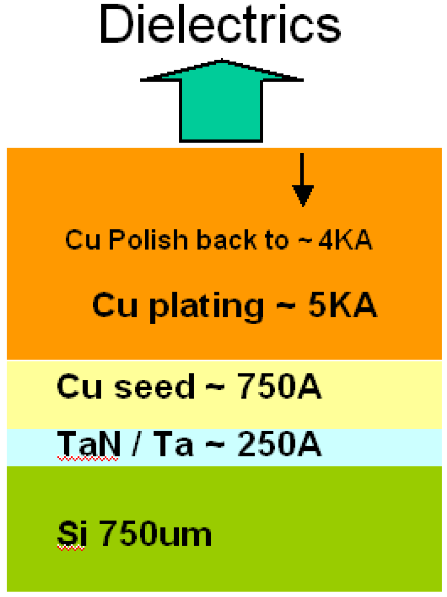
- SIMs:Second Ion Mass Spectroscopy was used to measure the depth profile of Cu. Samples were prepared, as figure 1, by physical vapor deposition 250 A TaN/Ta on a 750 µm bare silicon wafer. In order to provide copper electrochemical plating 5000A, the wafers were deposited with a 750A copper seed layer by physical vapor deposition. After chemical mechanical polishing back to 4000A, all dielectric samples were deposited.

| Sample identification | 4MS | 3MS | TEOS a | ||
|---|---|---|---|---|---|
| N a-SiCN:H | N a-SiCO:H | A a-SiCN:H | SiCO:H | PEOX | |
| Pressure (torr) | 2.0~3.0 | 3.0~4.0 | 1.5 | ||
| HFRF b | 550~600 | 450~600 | 200 | ||
| LFRF b | 900 | - | 0 | 80 | 800 |
| N/Si ratio | 2.06 | - | 1.84 | - | - |
| C/Si ratio | - | 6.55 | - | - | - |
| O/Si ratio | - | - | - | 2.0 | 12,000 |

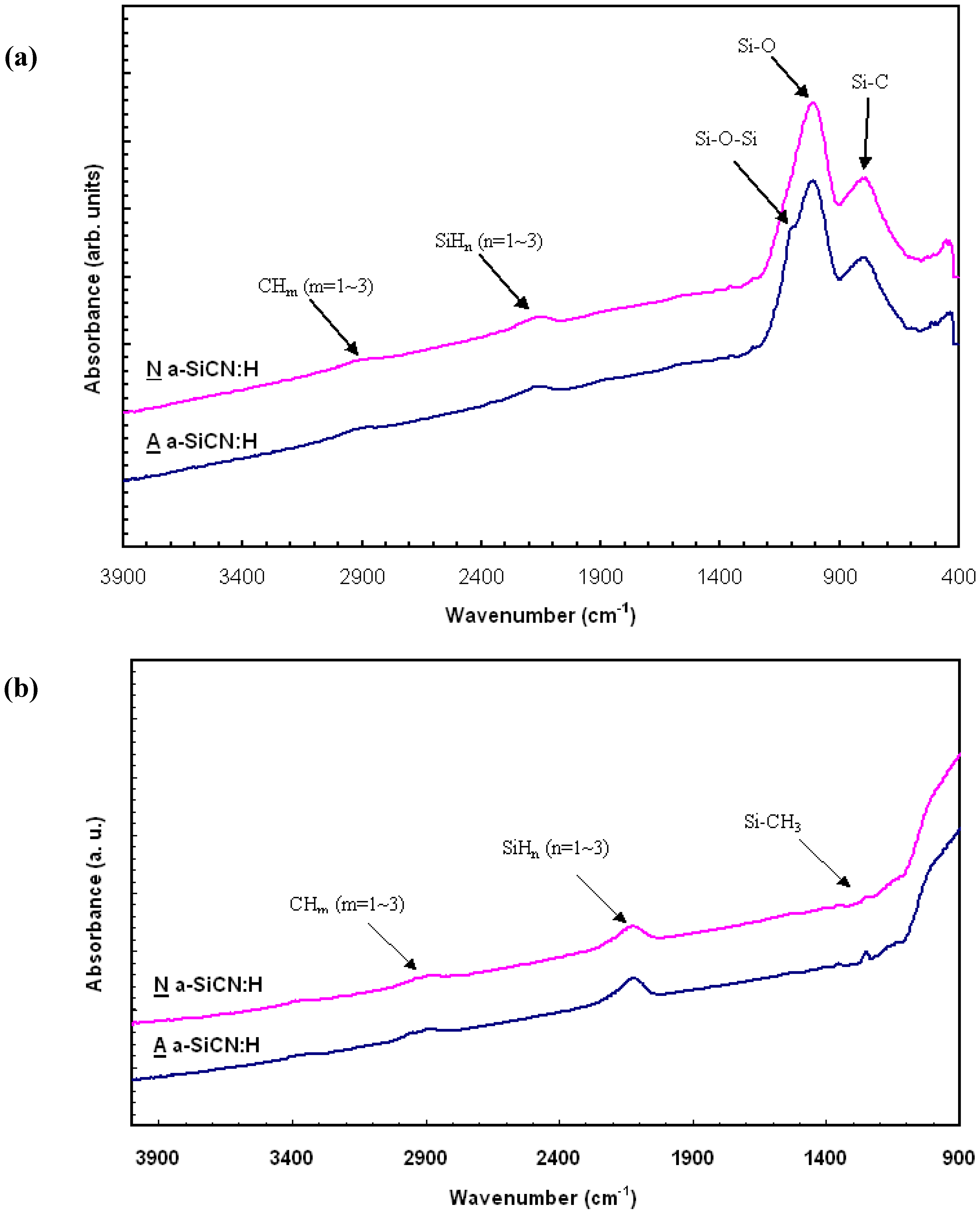
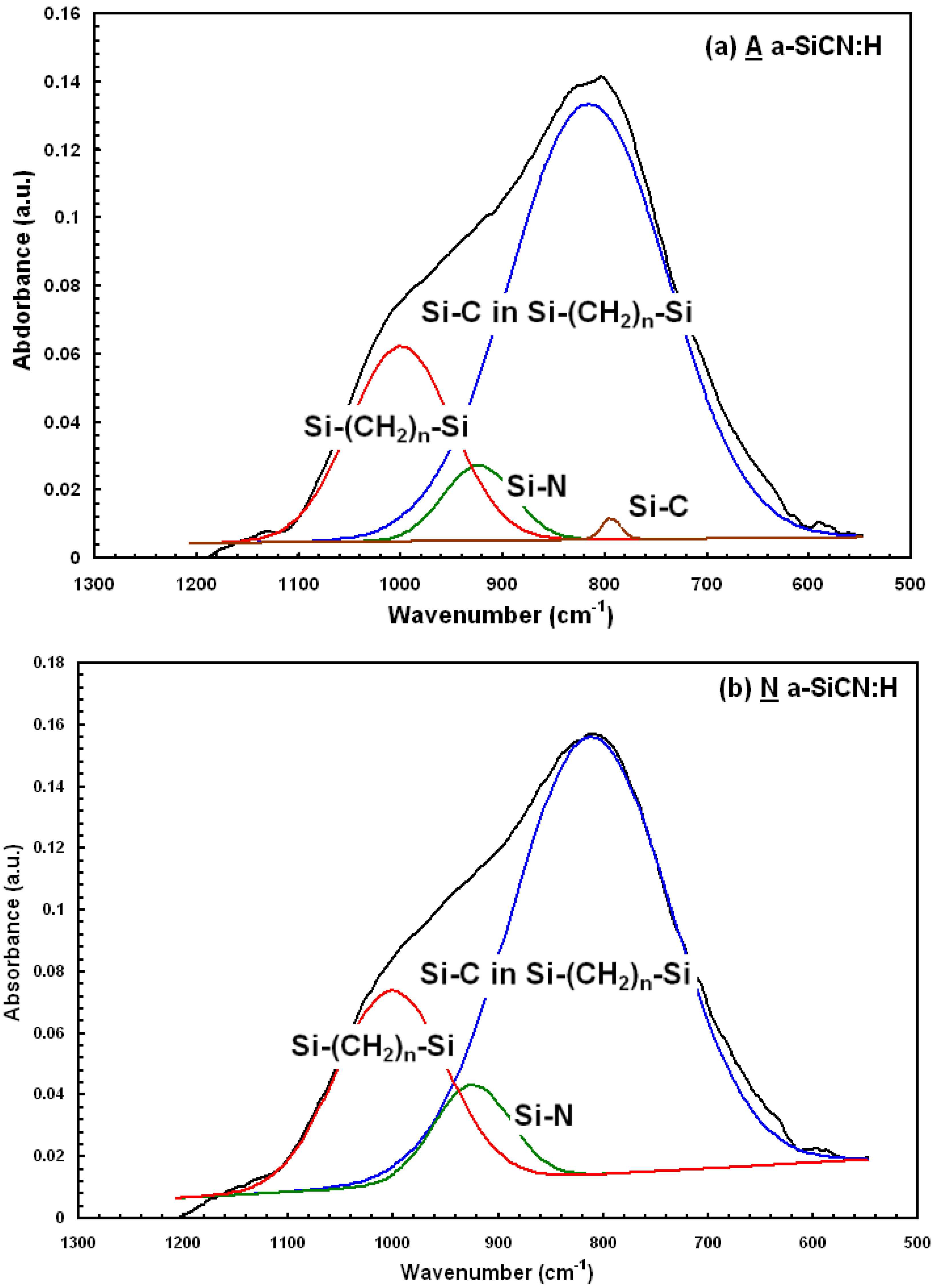
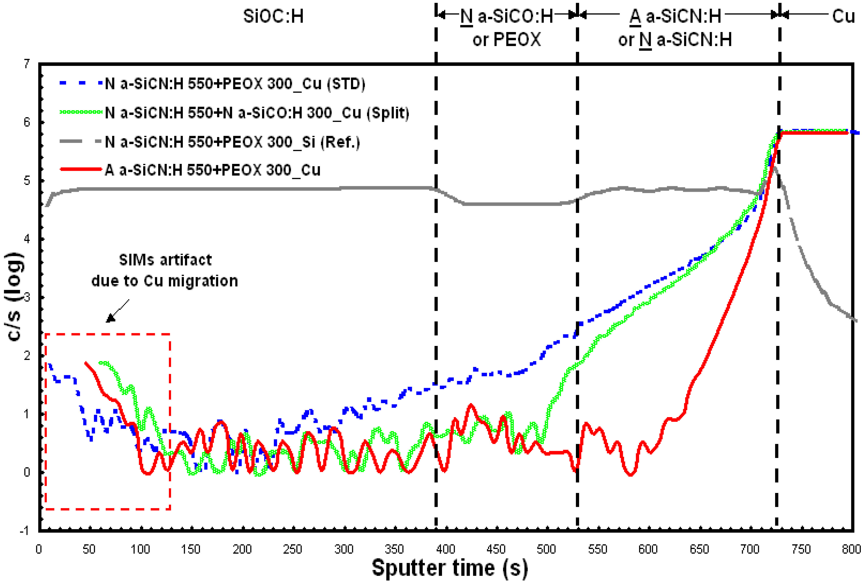
3. Results and Discussion
| Sample Condition | Thickness | K | |
|---|---|---|---|
| Optical | Electrical | ||
| 0SiOC:H | 387 nm | 498 nm | 3.04 |
| 1 A α-SiCN:H | 55 nm | 44 nm | 4.81 |
| 2 N α-SiCN:H | 57 nm | 39 nm | 5.68 |
| 3 N α-SiCO:H | 30 nm | 26 nm | 4.46 |
| 4 PEOX | 30 nm | 28 nm | 4.23 |
| N α-SiCN:H + PEOX + SiOC:H | 470 nm | 540 nm | 3.41 |
| N α-SiCN:H + N α-SiCO:H + SiOC:H | 470 nm | 544 nm | 3.39 |


4. Conclusions
Acknowledgments
References
- Schurr, M.; Brandl, D.; Tomaschko, Ch.; Schoppmann, Ch.; Voit, H. Langmuir—Blodgett films made from yttrium arachidate. Thin Solid Films 1995, 261, 271–274. [Google Scholar]
- Chiang, C.C.; Chen, M.C.; Ko, C.C.; Wu, Z.C.; Jang, S.M.; Liang, M.S. Physical and barrier properties of plasma-enhanced chemical vapor deposited α-SiC:H films from trimethylsilane and tetramethylsilane. Jpn. J. Appl. Phy. 2003, 42, 4273–4277. [Google Scholar] [CrossRef]
- Chang, S.Y.; Chang, J.Y.; Lin, S.J.; Tsai, H.C.; Chang, Y.S. Interface chemistry and adhesion strength between porous sioch low-k film and sicn layers. J. Electrochem. Soc. 2008, 155, G39–G43. [Google Scholar] [CrossRef]
- Ishii, A.; Matsumoto, S.; Hattori, T.; Suzuki, S.; Isono, S.; Iwasaki, A.; Tomita, K.; Hashimoto, K.; Tawa, S.; Furusawa, T.; et al. Interface engineering for highly-reliable 65 nm-node Cu/ULK (k = 2.6) interconnect integration. In Proceedings of the IEEE 2005 International Conference, Burlingame, CA, USA, 2005; pp. 21–23.
- Chen, C.W.; Chang, T.C.; Liu, P.T.; Tsai, T.M.; Tseng, T.Y. Effects of oxygen plasma ashing on barrier dielectric SiCN film. Electrochem. Solid-State Lett. 2005, 8, G11–G13. [Google Scholar] [CrossRef]
- Hatano, M.; Usui, T.; Shimooka, Y.; Kaneko, H. EM lifetime improvement of Cu damascene interconnects by p-SiC cap layer. In Proceedings of the IEEE 2002 International Conference, Burlingame, CA, USA, 7 August 2002; pp. 212–214.
- Cui, H.; Burke, P.A. Time-dependent dielectric breakdown studies of PECVD H:SiCN and H:SiC thin films for copper metallization. J. Electrochem. Soc. 2004, 151, G795–G800. [Google Scholar] [CrossRef]
- Tsui, B.Y.; Fang, K.L.; Lee, S.D. Electrical instability of low-dielectric constant diffusion barrier film (a-SiC:H) for copper interconnect. IEEE Trans. Electron. Devices 2001, 48, 2375–2383. [Google Scholar] [CrossRef]
- Nakamura, N.; Takigawa, Y.; Soda, E.; Hosoi, N.; Tarumi, Y.; Aoyama, H.; Tanaka, Y.; Kawamura, D.; Ogawa, S.; Oda, N.; Kondo, S.; Mori, I.; Saito, S. Design impact study of wiring size and barrier metal on device performance toward 22 nm-node featuring EUV lithography. In Proceedings of the Interconnect Technology Conference, Sapporo, Hokkaido, Japan, 2009; pp. 14–16.
- Zhang, D.H.; Yang, L.Y.; Li, C.Y.; Lu, P.W.; Foo, P.D. Ta/SiCN bilayer barrier for Cu-ultra low k integration. Thin Solid Films 2006, 504, 235–238. [Google Scholar] [CrossRef]
- Biggerstaff, T.L.; Reynolds, C.L.; Zheleva, T.; Leis, A.; Habersat, D.; Haney, S.; Ryu, S.H.; Agarwi, A.; Duscher, G. Relationship between 4H-SiC/SiO2 transition layer thickness and mobility. Appl. Phys. Lett. 2009, 95, 032108–032110. [Google Scholar] [CrossRef]
- Hu, C.K.; Rosenberg, R.; Rathore, H.S.; Nguyen, D.B.; Agarwala, B. Scaling effect on electromigration in on-chip Cu wiring. In Proceedings of the Interconnect Technology, San Francisco, CA, USA, 24–26 May 1999; pp. 267–269.
- Chen, C.W.; Liu, P.T.; Chang, T.C.; Yang, J.H.; Tsai, T.M.; Wu, H.H.; Tseng, T.Y. Cu-penetration induced breakdown mechanism for a-SiCN. Thin Solid Films 2004, 469–470, 388–392. [Google Scholar] [CrossRef]
© 2012 by the authors. Licensee MDPI, Basel, Switzerland. This article is an open access article distributed under the terms and conditions of the Creative Commons Attribution license ( http://creativecommons.org/licenses/by/3.0/).
Share and Cite
Chen, S.-W.; Wang, Y.-S.; Hu, S.-Y.; Lee, W.-H.; Chi, C.-C.; Wang, Y.-L. A Study of Trimethylsilane (3MS) and Tetramethylsilane (4MS) Based α-SiCN:H/α-SiCO:H Diffusion Barrier Films. Materials 2012, 5, 377-384. https://doi.org/10.3390/ma5030377
Chen S-W, Wang Y-S, Hu S-Y, Lee W-H, Chi C-C, Wang Y-L. A Study of Trimethylsilane (3MS) and Tetramethylsilane (4MS) Based α-SiCN:H/α-SiCO:H Diffusion Barrier Films. Materials. 2012; 5(3):377-384. https://doi.org/10.3390/ma5030377
Chicago/Turabian StyleChen, Sheng-Wen, Yu-Sheng Wang, Shao-Yu Hu, Wen-Hsi Lee, Chieh-Cheng Chi, and Ying-Lang Wang. 2012. "A Study of Trimethylsilane (3MS) and Tetramethylsilane (4MS) Based α-SiCN:H/α-SiCO:H Diffusion Barrier Films" Materials 5, no. 3: 377-384. https://doi.org/10.3390/ma5030377