Recent Progress in Two-Dimensional Nanomaterials for Laser Protection


Key Lab for Advanced Materials, School of Chemistry and Molecular Engineering, East China University of Science and Technology, 130 Meilong Road, Shanghai 200237, China
*
Authors to whom correspondence should be addressed.
Chemistry 2019, 1(1), 17-43; https://doi.org/10.3390/chemistry1010004
Submission received: 7 December 2018
/
Revised: 14 January 2019
/
Accepted: 15 January 2019
/
Published: 16 January 2019
(This article belongs to the Section Chemistry at the Nanoscale)
Abstract
:The Nobel Prize in Physics 2018, “For groundbreaking inventions in the field of laser physics”, went to Arthur Ashkin and Gérard Mourou and Donna Strickland. Their inventions have revolutionized laser physics and greatly promoted the development of laser instruments, which have penetrated into many aspects of people’s daily lives. However, for the purpose of protecting human eyes or optical instruments from being damaged by both pulsed and continuous wave laser radiation, the research on laser protective materials is of particular significance. Due to the intriguing and outstanding physical, chemical, and structural properties, two-dimensional (2D) nanomaterials have been extensively studied as optical limiting (OL) materials owing to their broadband nonlinear optical (NLO) response and fast carrier relaxation dynamics that are important for reducing the laser intensity. This review systematically describes the OL mechanisms and the recent progress in 2D nanomaterials for laser protection.
1. Introduction
The 2018 Nobel Prize in Physics went to Arthur Ashkin and Gérard Mourou and Donna Strickland, for groundbreaking inventions in the field of laser physics. Arthur Ashkin was awarded for his work with optical tweezers and their application in biological systems, Gérard Mourou and Donna Strickland were awarded for their method of generating high-intensity, ultra-short optical pulses (Figure 1a) [1,2,3,4,5,6,7]. By using optical tweezers, scientists can grasp particles, atoms, viruses, and even living bacteria without harming them [8,9,10,11,12]. Their inventions have revolutionized laser physics and have paved the way for the development of many disciplines in the past three decades, especially in the fields of biology, chemistry, and medicine [13,14,15,16,17]. As shown in Figure 1b, the interactions between photons and atoms include absorption of radiation, spontaneous emission, and stimulated emission [18,19,20]. The stimulated emission was first introduced by Albert Einstein in 1917 [21,22]. The process that electrons transit from the excited state to the ground state will release photons. However, when an electron is irradiated by an incoming photon and the energy of the incoming photon is exactly equal to the bandgap of the electron, the electron will immediately return to the ground state and then release two outgoing photons which have exactly the same energy as the incoming photon. Laser, light amplification of stimulated emission of radiation, originates from the stimulated emission process. In 1960, Maiman developed the first solid-state laser instrument, the Ruby laser, which uses a synthetic ruby crystal as the laser medium [23]. After that, the semiconductor laser instrument, gas laser instrument and the most common yttrium aluminum garnet (YAG) laser instrument were also invited. As shown in Figure 1c, due to the extraordinary and unique properties, lasers have triggered a surge of research attention in both fundamental studies and practical applications. The long optical path and the very small divergence angle enable the excellent directionality of lasers, which can be used in laser guidance, laser ranging, and optical discs. When a laser beam is focused on the surface of an object, its high brightness can make the surface temperature reach a much higher value than that of the surface of the sun, which can be applied in laser cutting, nuclear fusion, and internal carving. Other important applications of lasers are fiber optic communication and holography, owing to their brilliant coherence, which can be presumably understood as the consistency of frequency and phase.
Undoubtedly, lasers have greatly promoted scientific progress, but we should not neglect the potential danger caused by radiation. Table 1 summarizes the pathological effect caused by lasers at different wavelengths. Continuous laser light can possess power ranging from 0.001 to thousands of watts and pulsed laser can reach to millions of watts per fraction of a second. When a laser beam is focused at a point, the intensity can reach 105 times higher than that of the beam itself. Lasers used in weapons can readily stun or permanently blind human eyes and destroy optical sensors, missiles, and other targets. Lasers also have some common applications in our daily lives, such as reporters using a laser pointer when making a speech or supermarket staff using a cash register scanner to scan barcodes. For the purpose of protecting human eyes and optical instruments from being damaged by both pulsed and continuous wave laser radiation, research on laser protective materials has emerged. Optical limiting (OL) is a nonlinear optical (NLO) phenomenon, defined as a higher transmittance for incident light with a lower intensity and a significantly reduced transmittance for high-intensity incident light [24,25]. An ideal optical limiter can effectively attenuate the potentially dangerous high-intensity laser beam to a range that human eyes or optical instruments can withstand without affecting the observation.
In the past three decades, significant research efforts have been devoted to the study of nonlinear optics. Before 2010, research interests were mainly focused on the materials of fullerenes, carbon nanotubes, porphyrins, and phthalocyanines. Since 2010, most active areas in OL materials gradually shifted to two-dimensional materials. The ground-breaking discovery of graphene, and other ultrathin two-dimensional (2D) nanomaterials, has triggered a surge of research interest in both fundamental studies and potential applications owing to its intriguing and outstanding physical, chemical, and structural properties [26,27,28,29,30]. Figure 2 displays the typical graphene-like ultrathin 2D nanomaterials. These atomic-scale thick materials have a large surface area and outstanding thermal and electrical conductivity, superior flexibility, and superior nonlinear optical response, endowing it with the promising application scope in the field of supercapacitors [31,32,33,34], energy storage devices [35,36,37,38], organic light-emitting diodes (OLEDs) [39,40,41], information storage devices [42,43,44,45], optical limiters, [46,47,48,49,50,51,52,53] and others. Due to the extended conjugate sp2 π-system and linear dispersion relation of its electronic band structure, graphene, the most representative 2D nanomaterial, and its derivatives, possesses the ultra-broadband resonate NLO response and the ultrafast carrier relaxation dynamics, which make it suitable for the preparation of solution- or solid-state optical limiters. In addition to graphene, the other nanomaterials in the big 2D family, such as black phosphorus (BP) [54,55,56], antimonene [57], hexagonal boron nitride (h-BN) [58,59], halide perovskites [60,61,62], transition metal dichalcogenides (TMDs) [63,64], metal oxides [65,66], layered double hydroxides (LDHs) [67,68], and metal−organic frameworks (MOFs) [69,70] have also been extensively studied as OL materials. Different two-dimensional materials have different physical, chemical, and surface structures, which in turn lead to different functions and applications. For example, graphene has a zero bandgap, which can be used to replace metal as an electrode material, while BP has a tunable thickness-dependent bandgap and is an excellent semiconductor material, which can be used to prepare photovoltaic devices such as memory devices and solar cells [71,72,73]. However, the inter- and intra-molecular interactions of 2D nanomaterials can greatly shorten the excited state lifetime, add relaxation pathways, and thereby reduce effective NLO absorption [74,75,76]. Besides, these 2D materials usually exhibit notorious solubility and stability. Moreover, although significant progress has been made in the construction of solution- or solid-state optical limiters, considerable challenges still remain in both theoretical and experimental studies. For example, the laser wavelength coverage (180 nm to 1 mm, commonly in the visible and near-infrared regions) is so wide that no one single material can effectively protect against wide-spectrum laser attacks. In addition, the difficulties in detecting laser attacks (most laser frequencies are invisible to the naked eye) render an almost zero evasion time. To address these problems, it would be greatly desirable to explore the OL mechanisms of each material, and then design and synthesize new functional molecule/polymer for the non- and covalent functionalization of 2D materials by following the principle of nonlinear optics. Wide-spectrum laser protection can be achieved by modifying the molecular structure or electronic structure or crystal structure of the materials.
2. Optical Limiting Mechanisms
Decipherment of the underlying mechanisms for the OL behavior is of great importance to the quest for fundamental knowledge of photochemistry and physics, and, just as crucial, it will guide our endeavors to design novel OL materials, explore practical applications, and promote technological innovations for laser protection. In general, the most important mechanisms of optical limiting are nonlinear scattering (NLS), nonlinear absorption (NLA), and nonlinear refraction (NLR), in which NLA includes free carrier absorption (FCA), reverse saturable absorption (RSA), and multi-photon absorption (MPA) [77]. NLR, RSA, and FCA are caused by thermal effects deriving from the accumulative nonlinearities and depend on the energy fluence of the radiation deposited in the sample, while the MPA and NLR are caused by the instantaneous electronic effects and depend on the transient intensity of the incident laser. Different mechanisms cover different wavelength regions of laser irradiation. For example, the RSA behavior mainly covers the high-energy end of the visible, ranging from 400 nm to 600 nm, while the NLS behavior has influence in the visible and near-infrared region and the MPA works in the low-energy end of the visible, ranging from 600 nm to 800 nm. However, for practical and commercial purposes, it is highly desirable to synthesize the state-of-art OL materials, which can effectively combine different OL mechanisms in one OL chromophores system. By capturing the essence of each OL mechanism and the protective region of each OL chromophore, endeavors can creatively design ultra-broadband OL materials. Herein, we are going to illustrate the OL mechanisms in details.
2.1. Reverse Saturable Absorption
Phthalocyanines, porphyrins, fullerenes, and graphene exhibit excellent RSA effects for laser pulses at the high energy end of the visible, ranging from 400 nm to 600 nm. In a molecular system, materials exhibit increased transmission with increasing pulse energy, this is known as saturable absorption (SA). For SA, the singlet and/or triplet excited state absorption cross sections are usually smaller than the ground state absorption cross section, and the mechanism can be assigned to the one-photon absorption. The opposite situation, the decreased transmission with increasing pulse energy, is termed RSA. When the singlet and/or triplet excited state absorption cross sections are much larger than that of the ground state, the RSA takes place. In light of elucidating the working mechanism of the RSA process, a five-level system energy level model is introduced to simulate the RSA process in graphene, in which the vibrational levels of the electronic states are ignored. As depicted in Figure 3, by initial excitation, electrons in the ground state S0 can jump to the first excited singlet state S1. If the pulse duration of the laser is shorter than the interband relaxation time of the materials, electrons in the populated S1 will be further excited to S2 and then quickly relax to S1. Once returned to S1, the population may undergo an intersystem crossing to the first excited triplet T1 in the time of τisc and then the excited transition and relaxation between T1 and T2 will take place. After that, due to the longer time of T1 (τph) than τisc, the electron population is cyclically exchanged between the S1 and T1.
The previously mentioned electron transition process can be described by the following differential rate equations (in order to simplify the equations, the relaxation process of the S2 and T2 and the stimulated emission of the S1 can be ignored. The former is due to the rapid relaxation process and the latter is due to the small fluorescence quantum yield):
where ni (i = 1, 2, 3) is the populations of Si and Ti, σi (I = 0, S, T) is the absorption cross sections of S0, S1, and T1. The propagation equation (Equation (4)) can be introduced to explain the extinction process of the laser beam, in which the absorption coefficient α contains the excited-state absorption from S1 to T1. Since the lifetimes of some molecular system, such as phthalocyanine and porphyrin system, are much shorter than the pulse width (usually a nanosecond), the time derivatives in Equations (1)–(3) can be set to zero under the steady-state approximation. So, deriving from the Equations (1)–(4), the intensity-dependent absorption coefficient and the saturation intensity can be described by
where κ = σex/σ0 and σex is the absorption cross section of excited transitions, representing the degree of nonlinear absorption, is the photon energy. From Equation (5), the larger the κ values and the smaller the values are, the better the optical limiting performance is [78]. By using this five-level system energy level model, it can be clearly seen that the excited state absorption plays an important role in the RSA process.
2.2. Multi-Photon Absorption
Usually, when the bandgap of the optical limiting materials is larger than the photon energy of the pulse laser, multi-photon absorption takes place. Many conjugated polymers, organic chromophores, and graphene derivatives possess significant two-photon absorption (TPA) cross section, which can be used to realize the OL application [79]. As shown in Figure 4, MPA is the process that occurs in the medium by absorbing more than one photon simultaneously through the virtual states. Among MPA, the most common absorption is TPA and can be described by the “Beer–Lambert” equation:
where α in the unit of m−1 is the linear absorption coefficient, β in the unit of m/W is the nonlinear absorption coefficient. In most TPA cases, the linear absorption is negligible at low incident intensity, so the TPA process can be described by the following equations:
where L is the pathlength of the materials, I0 is the incident intensity, β0 is a constant called the non-saturation TPA coefficient and Is is the TPA-induced saturable intensity. Equation (8) is called the non-saturation model; Equation (9) applies for the hyperbolic saturation model for semiconductor materials; Equation (10) and Equation (11) stand for the TPA saturation in homogeneously and inhomogeneously broadened materials, respectively. By introducing these equations into Equation (7), it can be inferred that the transmission intensity decreases with the pulse intensity increasing, suggesting the OL behavior takes place. And the TPA-induced OL behavior strongly relies on the L, the pulse intensity and the TPA coefficient. In addition, the imaginary part of the third-order NLO susceptibility Imχ(3) is related to β by the equation:
where c is the light speed, is the wavelength of the incident laser, and n is the refractive index. Usually, the TPA process applies to the pulse wavelength ranging from 600 to 800 nm, which is the low energy end of the visible. So, to obtain the largest OL response in the visible region, it is highly desirable to design and synthesize the OL chromophores containing both TPA and RSA for practical OL limiters.
2.3. Free-Carrier Absorption
Free-carrier absorption usually applies to the semiconductor system, and the carriers arise from the photon excitation [80]. Figure 5 illustrates the FCA process, by absorbing the photon energy, the electron will be excited to the higher conductive band and the hole will go to the lower valence band. In a FCA system, there are four possible processes for the OL behavior, namely, linear absorption (the absorption coefficient is linear with the transmittance), TPA (two-photon absorption), one-photon (ground state absorption), and two-photon (excited state absorption) induced FCA. In which the simplest case is the linear absorption and can be described by the following equations:
where σFCA is the FCA cross section, T0 is the linear transmission. Equation (14) refers to the formula of carrier density N. It can be inferred from Equation (15) that the larger the peak incident fluence F0 is, the smaller the total transmission T is, resulting in the OL response. For the most sophisticated case, which contains the four possible processes in a FCA system, these equations are transformed into:
For the FCA-induced OL response, the pulse duration of the incident light is shorter than the diffusion and recombination time of free carriers, so the duration time has no influence on the FCA process. Besides, the generation of carriers are derived from the TPA process; however, there would be a competitive relationship between FCA and TPA processes in some semiconductor nanoparticles.
2.4. Nonlinear Scattering
Nonlinear scattering plays the most common role for the NLO response in the dispersion of nanomaterials. Graphene and its derivatives, the most representative materials in the ultrathin two-dimensional (2D) nanomaterials family, have been extensively studied as OL materials [48,49]. So, here we take graphene and its derivatives as examples to illustrate the NLS mechanism in detail. The thermally induced NLS is considered to be the primary mechanism for graphene-based nanomaterial dispersions [81,82]. Figure 6 shows that the intensity of a laser beam can be reduced by scattering it in large spatial dimensions. According to the Mie scattering theory, the effective OL behavior must be resulting from the formation of a larger scattering center, which means the size of the scattering center is in the same order of the wavelength of the laser radiation. In graphene dispersion, there are two sources of the induced scattering centers: the formation and growth of solvent bubbles, as a result of the thermal energy transfer from graphene to solvent; and the formation and expansion of microplasmas, which is due to the ionization of graphene nanosheet. The physical properties of the solvent will also have an influence on the OL behavior of the graphene dispersion. Usually, in some solvents with a low boiling point and low surface tension, better and faster OL performance and lower limiting threshold could be achieved. The relevant work has been reported by Wang et al. [83], they demonstrated that the surface tension of the solvent has more impact on the OL performance of carbon nanoparticles than the viscosity or the boiling point. In order to evaluate the diameter of the solvent bubbles, a simple model was established:
where γ is the surface tension, n is the number of moles of gas, R is the universal gas constant, T is the absolute temperature in the bubble, p is the pressure far from the bubble, and r is the radius of the bubble at the end of a laser pulse.
Belousova et al. also developed a theoretical model to illustrate the NLS behavior of carbon-based nanomaterials dispersion by dividing the OL process into three steps [84]: the dynamics of the formation and growth of solvent bubbles; the Mie scattering of the expanding bubbles; and the nonlinear propagation process of the scattering medium. This model shows that with the size of the solvent bubbles increasing, the scattering cross section increases significantly and the absorption cross section gradually decreases until becoming negligible.
According to the “Beer–Lambert” law, the linear transmission T0 and decreased transmission TNLO can be applied to the following equations:
where δ0 is the linear extinction cross section, δNLO is the nonlinear extinction cross section. Equation (21) is the ratio of the linear and nonlinear extinction cross section. According to Mie scattering theory and the theoretical model by Belousova et al., the absorption cross section will become negligible with the extension of the solvent bubbles. So, the scattering cross section δ and the TNLO can be expressed as:
where and are the coefficients defined with Bessel function and its differentiation, , q and are an integer, the corresponding size parameters and the radius of the micro-scatters, respectively.
3. Two-Dimensional (2D) Nanomaterials for Optical Limiting
Due to the outstanding physical, chemical, electronic, and optical properties, ultra-thin 2D materials can be potentially utilized in a wide spectrum of applications, including catalysis, energy storage, sensors, biomedicine and electronics/optoelectronics, etc. In this section, we briefly summarize the recent process of 2D materials by categories on the utilization for optical limiting.
3.1. Graphene
Graphene and its derivatives have been widely used in the preparation of optical limiting materials due to the ultra-broadband resonate NLO response and the ultrafast carrier relaxation dynamics that are derived from its extended conjugate sp2 π-system and linear dispersion relation of its electronic band structure. Recent advances of graphene-based optical limiting materials have been summarized in a comprehensive review [48].
Most recently, Chen et al. innovatively designed and synthesized the chemically modified reduced graphene oxide materials with aggregation-induced emission (AIE) polymer for solid-state optical limiters [49]. As shown in Figure 7a, the AIE-active polymer PBFTB was synthesized with Suzuki coupling reaction. By converting the bromine group to azide group, the polymer PAHFTP was functionalized on the surface of reduced graphene oxide via nitrene chemistry. The solid-state PFTP-RGO film showed typical RSA response at both 532 and 1064 nm, indicating it could be the potential broadband OL materials. From Figure 7b, it can be clearly seen that the annealed PFTP-RGO/PMMA film has the lowest normalized transmittance (Tmin) under both 532 and 1064 nm irradiation, indicating the best OL performance. Moreover, Figure 7c showed the OL threshold (the input influence or energy at which the Tmin is 50% of the linear transmittance) and the nonlinear coefficients (βeff) of the samples. Under the laser intensity of 300 μJ, by comparison with RGO/PMMA and PFTP-RGO/PMMA film, the annealed PFTP-RGO/PMMA film obtained the lowest OL thresholds (1.44 J/cm2 at 532 nm and 1.08 J/cm2 at 1064 nm) and the largest nonlinear coefficients (296.79 cm/GW at 532 nm and 369.89 cm/GW at 1064 nm). These values are among the best of the reported graphene-based NLO materials, providing a new avenue for designing ultra-broadband OL materials.
3.2. Black Phosphorus
As a rising star among the 2D nanomaterials family, black phosphorus (BP) has been extensively investigated due to its outstanding, high electron/hole mobility, thickness-dependent tunable bandgap, large photon-to-electron quantum yields [85], superior thermodynamic stability, and broadband nonlinear optical response. Figure 8a,b shows the non-planar, puckered architecture of BP, which consists of fused hexagons of sp3-hybridized P atoms [86,87,88]. The STEM image shows the aesthetically pleasing lattice structure of BP. However, in the presence of oxygen, BP will rapidly degrade within the scope of hours. This lack of stability under ambient conditions severely undermines the application of BP, which is still a formidable challenge for researchers to conquer.
Fan et al. first reported the broadband NLO response in multi-layer BP nanoplatelets both in solution and solid state [89]. As shown in Figure 9a, the multi-layer BP nanosheets were obtained by liquid exfoliation from bulk BP crystal. For BP dispersions, characterized by the wide-band open-aperture Z-scan techniques, saturable absorption (SA) was observed under femtosecond at both 400 nm and 800 nm (Figure 9b–d). The achieved saturation intensity and normalized transmittance value were 455.3 ± 55 GW/cm2 and 27.6% at 400 nm, 334.6 ± 43 GW/cm2 and 12.4% at 800 nm. For BP/PMMA thin film, similar results were also observed under picosecond excitations at both 1562 nm and 1930 nm and the corresponding values were 18.54 MW/cm2 and 19.5% at 1563 nm, and 4.56 MW/cm2 and 16.1% at 1930 nm. By centrifuging at 3000 rpm to remove the multi-layer BP, the few-layer BP nanosheet was obtained by centrifuging the supernatant at 12000 rpm (Figure 10a). As shown in Figure 10b, Chu et al. demonstrated that the few-layer BP nanosheet also exhibited the SA behavior in NMP at 800 nm with pulse width of 100 fs [90]. By using few-layered BP as an electron donor and C60 as an electron acceptor, Yu et al. successfully prepared the donor–acceptor (D-A) type blends and embedded them in the poly(methylmethacrylate) (PMMA) matrix as a solid-state optical limiter [91]. Due to the thermal-induced intermolecular charge transfer effect between BP and C60, the annealed BP:C60/PMMA film showed an enhanced optical limiting response at 532 nm. The nonlinear coefficient, the limiting threshold, and the damage threshold were 241.73 cm/GW, 4.5 J/cm2, and 19.54 J/cm2, respectively (Figure 10c). This creative strategy for designing such novel D-A type blends offers new solutions for constructing the next generation optical limiters.
However, for large scale production, it is difficult to control the thickness and lateral size of BP nanosheets by liquid exfoliation. Ultrasmall quantum dots (QDs) are another morphology of 2D materials with a particle size less than the exciton Bohr radius. Due to the existence of the quantum-confinement effect, QDs usually exhibit some excellent physical and chemical properties, especially in the field of optoelectronics. As depicted in Figure 11a, by using the solvothermal method, Yu et al. successfully prepared the black phosphorus quantum dots (BPQDs) with an average size of 2.1 ± 0.9 nm from bulk BP crystal and used it as an optical saturable absorber [92]. The achieved saturable intensity and modulation depth were 3.3 GW/cm2 and 36% (Figure 11b). Similar results were also obtained by other researchers and these results demonstrate that BP and its derivatives could be an extraordinary candidate for ultrafast photonics devices. Furthermore, the work of non- and covalent functionalization of BP as OL materials is well worth exploring, especially the covalent functionalization, as it is considered to have better and more stable physicochemical properties than non-covalent modifications.
3.3. Antimonene
In contrast to the instability of BP in air, which has greatly limited the application scope of BP and its derivatives, antimonene, the group-VA element composed 2D material, was recently predicted to be of good stability [93]. Figure 12 illustrates the atomic structure of β-phase antimonene; the monolayer β-phase antimonene consists of buckled hexagonal rings composed of Sb atoms connected through sp3 bonding and the layer distance is about 0.38 nm. According to theoretical calculations, antimonene presents high carrier mobility, superior thermal conductivity, strain-induced band transition and promising spintronic properties [94,95,96,97,98]. Although the antimonene possesses these excellent properties, reports in the field of nonlinear optical are still scarce. Zhang et al. first reported the NLO response of few-layer antimonene decorated microfiber with the exciting source at 800 and 1500 nm, and the pulse duration is 95 fs and repetition rate is 1 kHz [99]. Figure 13b illustrates the evanescent field method of depositing few-layer antimonene nanoflakes onto a piece of microfiber. From Figure 13a, it can be seen that antimonene showed the typical SA response, and the achieved saturable intensity and modulation depth are 14.25 GW/cm2 and 3.96% at 800 nm and 15.10 GW/cm2 and 19.72% at 1500 nm. However, the RSA response of antimonene was observed by Xu et al. for the first time [100]. When the pulse energy was above 7.43 μJ excitation at 1064 nm, the competitive process between single photon absorption (1PA) and two-photon absorption (TPA) was observed (Figure 13c). The same phenomenon was also observed at the higher energy of visible region (532 nm), suggesting antimonene could be the TPA-dominant OL materials.
3.4. Hexagonal Boron Nitride Sheets (h-BN)
Hexagonal boron nitride (h-BN), which is called the “white graphene”, has a similar lattice structure to graphene (Figure 14a) [101]. However, in contrast to the zero bandgap of graphene, h-BN has a wide bandgap of about 6.1 eV at room temperature demonstrated by experimental and theoretical studies. Due to the high-temperature stability, outstanding mechanical strength, intrinsic electrical insulation and anti-oxidation capacity [102,103,104], h-BN may have the potential of being a nonlinear optical material. The NLO properties of h-BN dispersion were first studied by Ajayan et al. and the typical OL response was observed at 1064 nm with the pulse duration of 10 ns [105]. The tested data fitted well with the TPA and the largest achieved TPA coefficient was 74.84 cm/GW at the peak intensity of 0.02 GW/cm (Figure 14b). From a practical application point of view, it is better to fabricate solid-state optical limiters by embedding the NLO materials as inclusions in a suitable non-optically active host and/or polymerizing the NLO chromophore-based monomers to form composite functional materials [49]. Hao et al. investigated the NLO response of h-BN nanosheets (BNNSs) in both solution and solid state [106]. The MTES hybrid gel glasses of BNNSs were successfully prepared by the modified molten hydroxide exfoliation method and the Z-scan test was performed at 532, 1064, and 2000 nm (Figure 15a). By comparison with carbon nanomaterials (i.e., graphene and graphene oxide), the BNNSs showed superior OL performance both in solution and solid state which can be explained by the good transparency, high thermal conductivity, and stability of BNNSs. Meanwhile, due to the long-term optical, thermal, and mechanical stability of the ormosil glasses, the MTES hybrid gel glasses of BNNSs have a better performance than BNNSs dispersion. The ultra-broadband NLO response of h-BN, ranging from 500 to 2000 nm, were deduced from the combination of NLA, NLS, and NLR, indicating h-BN could be another promising OL material after graphene.
3.5. Transition Metal Dichalcogenides (TMDs)
Transition Metal Dichalcogenides (TMDs), of which the general formula is MX2 (M=Mo, W, Nb, Ta; X = S, Se), is analogous to graphene and has a layered structure [27]. The TMD monolayer structure contains three atomic layers and the middle layer is the transition metal layer. The layered TMDs crystals are stacked by the van der Waals force and the most characteristic feature of TMDs is their capability to form different crystal polytypes. MoS2, as the prototypical TMD, has five different crystal structures, naming 1H, 1T, 1T′, 2H, and 3R (Figure 16a). Due to the different crystal polytypes, ultrafast carrier dynamics, and ultrafast nonlinear absorption, much attention has been focused on the study of nonlinear optical properties of TMDs. Wang et al. systematically investigated the NLO behavior of MoS2, MoSe2, WS2, WSe2, and graphene nanosheets with the excitation wavelength of 532 and 1064 nm [107]. Both TMDs and graphene strong optical limiting responses at 1064 nm, which originated from the NLS (Figure 16b). However, at 532 nm, the TMDs showed a combination of SA and NLS response. Among these materials, the performance of the selenium compounds is superior to the sulfide compounds in the near infrared region. However, little work has focused on the impact of different crystal structure on the electronic and optical properties. As the most stable phase at ambient conditions, the 2H phase TMDs have been widely used in transistor devices. While the less stable 1T’ phase exhibits some unique properties, such as dipolar ferroelectricity, Weyl semimetal, and quantum spin Hall effect, et al. [108,109,110,111].
By intercalating the alkali metal hydrides, which served as the electron donors, the complete phase conversion from 2H-to-1T′ took place and the 1T′ phase of MoS2 and WS2 showed unprecedented long-term stability in the ambient environment [112]. Under the excitation of a femtosecond laser at 900 nm, the 1T′ phase few-layered h-LiMoS2 exhibited the typical SA response, while the 2H phase MoS2 showed SA at a low energy level and TPA behavior in the high energy region (Figure 17). The nonlinear optical studies revealed that the 1T’ phase TMDs had a much higher conduction band electron occupancy, optical transparency, and optical Kerr nonlinearity effect, allowing the 1T’ phase TMDs promising for nonlinear photonic applications.
3.6. Halide Perovskites
Halide perovskites, with the general crystal structure formula of ABX3 (A = organic ammonium cation, Cs+; B = Pb2+, Sn2+; X = Cl, Br, I), present some excellent optical and electrical properties such as low-temperature solution processability, long photocarrier lifetime, high fluorescence yield, wavelength tenability, and nonlinear response [113,114,115,116]. These unique and exciting properties make perovskites promising for application in optoelectronic devices, especially in photovoltaic operation and laser protection [117,118,119,120,121,122,123]. Figure 18a depicts the key structural factors of halide perovskites, these factors can form different properties of halide perovskites, such as absorption properties, the emission wavelength and charge carrier lifetimes, etc. Similar to TMDs, halide perovskites also have three different crystal structures of 100, 110, and 111 (Figure 18b), which can be used to construct different formations for its potentially diverse varieties of practical applications.
The NLO response of organic−inorganic perovskites absorbers CH3NH3PbI3 was investigated by Snaith et al. and the typical SA was observed under the excitation of both 532 and 1064 nm [124]. The achieved nonlinear absorption coefficient and saturable intensity were −2.25 cm/MW, 12.71 GW/cm2 for CH3NH3PbI3 and −2.03 cm/MW, 12.61 GW/cm2 for CH3NH3PbI3−xClx, respectively (Figure 19a,b). The same OL response was also observed in the CH3NH3PbI3 perovskite nanosheets, in which the thickness was about 105 nm [123]. The achieved highest normalized transmittance value was 22.2% and the lowest saturable intensity was about 1.8 × 10³ GW/cm, which is much larger than the bulk perovskite sheets. By embedding the CH3NH3PbI3 film into the ring fiber laser, the organic–inorganic halide perovskites hybrid was prepared and showed the saturable absorption coefficients of the normalized transmittance value and saturable intensity were 13.58% and 6.4 MW/cm2, respectively [126]. All of these results suggest that the perovskites could find important applications in ultrafast photonics as a new type of NLO material.
4. Conclusion and Perspectives
The Nobel Prize in Physics 2018 revealed the particular significance of lasers for civilian, industrial, military, and medical purposes. As lasers are becoming more and more common in daily life, it is crucial to design and synthesize state-of-art broadband OL chromophores to prevent human eyes or optical instruments from being damaged by both pulsed and continuous wave lasers. Ultrathin 2D nanomaterials feature unprecedented physical, electronic, and chemical properties, and explosive progress has been achieved in the field of OL. However, the inevitable drawbacks cannot be ignored, such as the notorious dispersion ability and dispersion stability, high-yield and large scale production, thickness and crystal structure controlling ability, ambient stability, aggregation effect, etc. So, the study of 2D nanomaterials for OL is still in its infancy and is far from mature. Significant challenges still remain in both theoretical and experimental studies.
Although the study of 2D nanomaterials with superior NLO properties is one of the most active areas in laser protection, a single material cannot protect against the wide-spectrum laser and cover all the requirements of NLO applications. Following the principle of nonlinear optics, by taking the essence and discarding the dregs of every material, it is desirable to explore the chemical modification of the ultrathin materials, such as the non- and covalent functionalization. By modifying the molecular structure or electronic structure or crystal structure of the material, wide-spectrum laser protection can be achieved with the combination of two or more OL mechanisms. Furthermore, in the big 2D nanomaterials family, aside from the six nanomaterials mentioned here, others (i.e., covalent−organic frameworks (COFs), metal−organic frameworks (MOFs), MXenes) have been less studied and are well worth exploring in nonlinear optics, which could be the next-generation optical limiter. The transformation from solution-state to solid-state film can also provide new avenues for designing and fabricating industrially applicable optical limiters.
Future work on OL materials should be focused on (I) exploration of the new ultra-thin 2D nanomaterials (i.e., the new transition metal dichalcogenides PtSe2) in the preparation of OL materials; (II) design and synthesis of the new organic chromophores or polymers with unique properties (i.e., AIE-active, Vibration Induced Emission (VIE)-active) for the covalent functionalization of 2D nanomaterials; (III) exploration of a non-optically active matrix with excellent physical properties (i.e., flexibility, heat resistance, pressure resistance) that can be used for the construction of solid-state optical limiters; (IV) the in-depth study of solution and solid-state systems to provide a profound understanding of the nonlinear optical mechanisms; (V) exploration of the effect of different Z-scan system (i.e., the pulse duration (picosecond, femtosecond, nanosecond level), the pulse repetition rate).
Funding
We are grateful for the financial support of the National Natural Science Foundation of China (61378072).
Conflicts of Interest
The authors declare no conflict of interest.
References
- Ashkin, A. Optical trapping and manipulation of neutral particles using lasers. Proc. Natl. Acad. Sci. USA 1997, 94, 4853–4860. [Google Scholar] [CrossRef] [PubMed] [Green Version]
- Strickland, D.; Mourou, G. Compression of amplified chirped optical pulses. Opt. Commun. 1985, 56, 219–221. [Google Scholar] [CrossRef]
- Ashkin, A. Acceleration and Trapping of Particles by Radiation Pressure. Phys. Rev. Lett. 1970, 24, 156–159. [Google Scholar] [CrossRef]
- Ashkin, A.; Dziedzic, J.M. Optical Levitation by Radiation Pressure. Appl. Phys. Lett. 1971, 19, 283–285. [Google Scholar] [CrossRef]
- Ashkin, A.; Dziedzic, J.M.; Bjorkholm, J.E.; Chu, S. Observation of a single-beam gradient force optical trap for dielectric particles. Opt. Lett. 1986, 11, 288–290. [Google Scholar] [CrossRef] [PubMed]
- Desbois, J.; Gires, F.; Turnois, P. A new approach to picosecond laser pulse analysis shaping and coding. IEEE J. Quant. Electron. 1973, 9, 213–218. [Google Scholar] [CrossRef]
- The Nobel Prize in Physics 2018. NobelPrize.org. Nobel Media AB. Available online: https://www.nobelprize.org/prizes/physics/2018/press-release/ (accessed on 2 October 2018).
- Ashkin, A. Trapping of Atoms by Resonance Radiation Pressure. Phys. Rev. Lett. 1978, 40, 729–732. [Google Scholar] [CrossRef]
- Ashkin, A.; Dziedzic, J.M. Optical trapping and manipulation of viruses and bacteria. Science 1987, 235, 1517–1520. [Google Scholar] [CrossRef] [PubMed]
- Ashkin, A.; Dziedzic, J.M. Internal cell manipulation using infrared laser traps. Proc. Natl. Acad. Sci. USA 1989, 86, 7914–7918. [Google Scholar] [CrossRef]
- Ashkin, A.; Schütze, K.; Dziedzic, J.M.; Euteneuer, U.; Schliwa, M. Force generation of organelle transport measured in vivo by an infrared laser trap. Nature 1990, 348, 346–348. [Google Scholar] [CrossRef]
- Block, S.M.; Blair, D.F.; Berg, H.C. Compliance of bacterial flagella measured with optical tweezers. Nature 1989, 338, 514–518. [Google Scholar] [CrossRef] [PubMed]
- Abbondanzieri, E.A.; Greenleaf, W.J.; Shaevitz, J.W.; Landick, R.; Block, S.M. Direct observation of base-pair stepping by RNA polymerase. Nature 2005, 438, 460–465. [Google Scholar] [CrossRef] [PubMed] [Green Version]
- Perkins, T.T.; Quake, S.R.; Smith, D.E.; Chu, S. Relaxation of a single DNA molecule observed by optical microscopy. Science 1994, 264, 822–826. [Google Scholar] [CrossRef] [Green Version]
- Smith, S.B.; Cui, Y.; Bustamante, C. Overstretching B-DNA: The elastic response of individual double-stranded and single-stranded DNA molecules. Science 1996, 271, 795–799. [Google Scholar] [CrossRef]
- Sekundo, W.; Kunert, K.S.; Blum, M. Small incision corneal refractive surgery using the small incision lenticule extraction (SMILE) procedure for the correction of myopia and myopic astigmatism: Results of a 6 month prospective study. Br. J. Ophthalmol. 2011, 95, 335–339. [Google Scholar] [CrossRef]
- Lin, F.; Xu, Y.; Yang, Y. Comparison of the visual results after SMILE and femtosecond laser-assisted LASIK for myopia. J. Refract. Surg. 2014, 30, 248–254. [Google Scholar] [CrossRef] [PubMed]
- Pert, G.J. Output characteristics of amplified-stimulated-emission lasers. J. Opt. Soc. Am. B 1994, 11, 1425–1435. [Google Scholar] [CrossRef]
- Wang, H.; Yu, H.; Zhou, X.; Kan, Q.; Yuan, L.; Chen, W.; Wang, W.; Ding, Y.; Pan, J. High-power InGaAs/GaAs quantum-well laser with enhanced broad spectrum of stimulated emission. Appl. Phys. Lett. 2014, 105, 141101. [Google Scholar] [CrossRef]
- Apkarian, V.A. Stimulated emission as a major channel for the depopulation of laser-excited states in condensed media. Chem. Phys. Lett. 1984, 108, 150–154. [Google Scholar] [CrossRef]
- Hutchin, R.A. A New Physical Model for the Vacuum Field Based on Einstein’s Stimulated Emission Theory. Opt. Photon. J. 2015, 5, 109–112. [Google Scholar] [CrossRef]
- Johar Shakir, Q.J.; Patel, A.R. The use of lasers in periodontology. Int. J. Curr. Res. 2017, 9, 44806–44809. [Google Scholar]
- Maiman, T.H. Stimulated Optical Radiation in Ruby. Nature 1960, 187, 493–494. [Google Scholar] [CrossRef]
- Spangler, C.W. Recent development in the design of organic materials for optical power limiting. J. Mater. Chem. 1999, 9, 2013–2020. [Google Scholar] [CrossRef]
- Leite, R.C.C.; Porto, S.P.S.; Damen, T.C. The Thermal Lens Effect as a Power-Limiting Device. Appl. Phys. Lett. 1967, 10, 100–101. [Google Scholar] [CrossRef]
- Zhang, H. Ultrathin Two-Dimensional Nanomaterials. ACS Nano 2015, 9, 9451–9469. [Google Scholar] [CrossRef] [PubMed]
- Tan, C.; Cao, X.; Wu, X.J.; He, Q.; Yang, J.; Zhang, X.; Chen, J.; Zhao, W.; Han, S.; Nam, G.H.; et al. Recent Advances in Ultrathin Two-Dimensional Nanomaterials. Chem. Rev. 2017, 117, 6225–6331. [Google Scholar] [CrossRef] [PubMed]
- Xu, M.; Liang, T.; Shi, M.; Chen, H. Graphene-like two-dimensional materials. Chem. Rev. 2013, 113, 3766–3798. [Google Scholar] [CrossRef]
- Chen, Y.; Fan, Z.; Zhang, Z.; Niu, W.; Li, C.; Yang, N.; Chen, B.; Zhang, H. Two-Dimensional Metal Nanomaterials: Synthesis, Properties, and Applications. Chem. Rev. 2018, 118, 6409–6455. [Google Scholar] [CrossRef] [PubMed]
- Sun, Y.; Gao, S.; Xie, Y. Atomically-thick two-dimensional crystals: Electronic structure regulation and energy device construction. Chem. Soc. Rev. 2014, 43, 530–546. [Google Scholar] [CrossRef]
- Acerce, M.; Voiry, D.; Chhowalla, M. Metallic 1T phase MoS2 nanosheets as supercapacitor electrode materials. Nat. Nanotechnol. 2015, 10, 313–318. [Google Scholar] [CrossRef] [PubMed]
- Wu, H.; Yu, G.; Pan, L.; Liu, N.; McDowell, M.T.; Bao, Z.; Cui, Y. Stable Li-ion battery anodes by in-situ polymerization of conducting hydrogel to conformally coat silicon nanoparticles. Nat. Commun. 2013, 4, 1943. [Google Scholar] [CrossRef] [Green Version]
- Zhang, M.; Zhu, Y.; Wang, X.; Feng, Q.; Qiao, S.; Wen, W.; Chen, Y.; Cui, M.; Zhang, J.; Cai, C.; et al. Controlled Synthesis of ZrS2 Monolayer and Few Layers on Hexagonal Boron Nitride. J. Am. Chem. Soc. 2015, 137, 7051–7054. [Google Scholar] [CrossRef] [PubMed]
- Wang, L.; Lin, C.; Zhang, F.X.; Jin, J. Phase Transformation Guided Single-Layer β-Co(OH)2 Nanosheets for Pseudocapacitive Electrodes. ACS Nano 2014, 8, 3724–3734. [Google Scholar] [CrossRef] [PubMed]
- Roy-Mayhew, J.D.; Aksay, I.A. Graphene materials and their use in dye-sensitized solar cells. Chem. Rev. 2014, 114, 6323–6348. [Google Scholar] [CrossRef] [PubMed]
- Liu, Z.; Lau, S.P.; Yan, F. Functionalized graphene and other two-dimensional materials for photovoltaic devices: Device design and processing. Chem. Soc. Rev. 2015, 44, 5638–5679. [Google Scholar] [CrossRef]
- Wan, X.; Long, G.; Huang, L.; Chen, Y. Graphene—A promising material for organic photovoltaic cells. Adv. Mater. 2011, 23, 5342–5358. [Google Scholar] [CrossRef] [PubMed]
- Du, J.; Pei, S.; Ma, L.; Cheng, H.M. 25th anniversary article: Carbon nanotube- and graphene-based transparent conductive films for optoelectronic devices. Adv. Mater. 2014, 26, 1958–1991. [Google Scholar] [CrossRef]
- Puzzo, D.P.; Helander, M.G.; O’Brien, P.G.; Wang, Z.; Soheilnia, N.; Kherani, N.; Lu, Z.; Ozin, G.A. Organic light-emitting diode microcavities from transparent conducting metal oxide photonic crystals. Nano Lett. 2011, 11, 1457–1462. [Google Scholar] [CrossRef]
- Wu, T.L.; Yeh, C.H.; Hsiao, W.T.; Huang, P.Y.; Huang, M.J.; Chiang, Y.H.; Cheng, C.H.; Liu, R.S.; Chiu, P.W. High-Performance Organic Light-Emitting Diode with Substitutionally Boron-Doped Graphene Anode. ACS Appl. Mater. Interfaces 2017, 9, 14998–15004. [Google Scholar] [CrossRef]
- Kim, J.S.; Jeon, P.J.; Lee, J.; Choi, K.; Lee, H.S.; Cho, Y.; Lee, Y.T.; Hwang, D.K.; Im, S. Dual Gate Black Phosphorus Field Effect Transistors on Glass for NOR Logic and Organic Light Emitting Diode Switching. Nano Lett. 2015, 15, 5778–5783. [Google Scholar] [CrossRef]
- Zhang, B.; Liu, G.; Chen, Y.; Zeng, L.J.; Zhu, C.X.; Neoh, K.G.; Wang, C.; Kang, E.T. Conjugated polymer-grafted reduced graphene oxide for nonvolatile rewritable memory. Chem. Eur. J. 2011, 17, 13646–13652. [Google Scholar] [CrossRef] [PubMed]
- Fan, F.; Zhang, B.; Cao, Y.; Chen, Y. Solution-processable poly(N-vinylcarbazole)-covalently grafted MoS2 nanosheets for nonvolatile rewritable memory devices. Nanoscale 2017, 9, 2449–2456. [Google Scholar] [CrossRef] [PubMed]
- Sun, S.; Zhuang, X.; Liu, B.; Wang, L.; Gu, L.; Song, S.; Zhang, B.; Chen, Y. In Situ Synthesis and Characterization of Poly(aryleneethynylene)-Grafted Reduced Graphene Oxide. Chem. Eur. J. 2016, 22, 2247–2252. [Google Scholar] [CrossRef] [PubMed]
- Fan, F.; Zhang, B.; Cao, Y.; Yang, X.; Gu, J.; Chen, Y. Conjugated polymer covalently modified graphene oxide quantum dots for ternary electronic memory devices. Nanoscale 2017, 9, 10610–10618. [Google Scholar] [CrossRef] [PubMed]
- Liu, R.; Hu, J.; Zhu, S.; Lu, J.; Zhu, H. Synergistically Enhanced Optical Limiting Property of Graphene Oxide Hybrid Materials Functionalized with Pt Complexes. ACS Appl. Mater. Interfaces 2017, 9, 33029–33040. [Google Scholar] [CrossRef]
- Zhu, J.; Li, Y.; Chen, Y.; Wang, J.; Zhang, B.; Zhang, J.; Blau, W.J. Graphene oxide covalently functionalized with zinc phthalocyanine for broadband optical limiting. Carbon 2011, 49, 1900–1905. [Google Scholar] [CrossRef] [Green Version]
- Chen, Y.; Bai, T.; Dong, N.; Fan, F.; Zhang, S.; Zhuang, X.; Sun, J.; Zhang, B.; Zhang, X.; Wang, J.; et al. Graphene and its derivatives for laser protection. Prog. Mater. Sci. 2016, 84, 118–157. [Google Scholar] [CrossRef]
- Liu, Z.; Dong, N.; Jiang, P.; Wang, K.; Wang, J.; Chen, Y. Reduced Graphene Oxide Chemically Modified with Aggregation-Induced Emission Polymer for Solid-State Optical Limiter. Chem. Eur. J. 2018, 24, 19317–19322. [Google Scholar] [CrossRef]
- Shi, M.; Dong, N.; He, N.; Wan, Y.; Cheng, H.; Han, M.; Wang, J.; Chen, Y. MoS2 nanosheets covalently functionalized with polyacrylonitrile: Synthesis and broadband laser protection performance. J. Mater. Chem. C 2017, 5, 11920–11926. [Google Scholar] [CrossRef]
- Zhang, W.; Zhang, L.; Zhou, L.; Zhang, J.; Li, F.; Li, K.; Yang, H. An all-liquid crystal based high-performance laser protection system via linear/nonlinear dual-mechanisms. Chem. Commun. 2018, 54, 397–400. [Google Scholar] [CrossRef]
- Zhang, W.; Zhang, L.; Liang, X.; Le, Z.; Xiao, J.; Yu, L.; Li, F.; Cao, H.; Li, K.; Yang, Z.; et al. Unconventional High-Performance Laser Protection System Based on Dichroic Dye-Doped Cholesteric Liquid Crystals. Sci. Rep. 2017, 7, 42955. [Google Scholar] [CrossRef] [PubMed] [Green Version]
- Wang, L. Self-activating liquid crystal devices for smart laser protection. Liq. Cryst. 2016, 43, 2062. [Google Scholar] [CrossRef]
- Wang, K.; Szydlowska, B.M.; Wang, G.; Zhang, X.; Wang, J.J.; Magan, J.J.; Zhang, L.; Coleman, J.N.; Wang, J.; Blau, W.J. Ultrafast Nonlinear Excitation Dynamics of Black Phosphorus Nanosheets from Visible to Mid-Infrared. ACS Nano 2016, 10, 6923–6932. [Google Scholar] [CrossRef] [PubMed]
- Wang, Y.W.; Liu, S.; Zeng, B.W.; Huang, H.; Xiao, J.; Li, J.B.; Long, M.Q.; Xiao, S.; Yu, X.F.; Gao, Y.L.; et al. Ultraviolet saturable absorption and ultrafast carrier dynamics in ultrasmall black phosphorus quantum dots. Nanoscale 2017, 9, 4683–4690. [Google Scholar] [CrossRef]
- Huang, J.; Dong, N.; Zhang, S.; Sun, Z.; Zhang, W.; Wang, J. Nonlinear Absorption Induced Transparency and Optical Limiting of Black Phosphorus Nanosheets. ACS Photon. 2017, 4, 3063–3070. [Google Scholar] [CrossRef]
- Lu, L.; Tang, X.; Cao, R.; Wu, L.; Li, Z.; Jing, G.; Dong, B.; Lu, S.; Li, Y.; Xiang, Y.; et al. Broadband Nonlinear Optical Response in Few-Layer Antimonene and Antimonene Quantum Dots: A Promising Optical Kerr Media with Enhanced Stability. Adv. Opt. Mater. 2017, 5, 1700301. [Google Scholar] [CrossRef]
- Karamanis, P.; Otero, N.; Pouchan, C. Unleashing the quadratic nonlinear optical responses of graphene by confining white-graphene (h-BN) sections in its framework. J. Am. Chem. Soc. 2014, 136, 7464–7473. [Google Scholar] [CrossRef]
- Subrata, B.; Chandra, S.T.; Soumya, V.; Arup, K.K.; Udit, C.; Pathik, K.; Pulickel, M.A. Nonlinear Optical Properties and Temperature Dependent Photoluminescence in hBN-GO Heterostructure 2D Material. J. Phys. Chem. C 2017, 121, 8060–8069. [Google Scholar]
- Saouma, F.O.; Stoumpos, C.C.; Wong, J.; Kanatzidis, M.G.; Jang, J.I. Selective enhancement of optical nonlinearity in two-dimensional organic-inorganic lead iodide perovskites. Nat. Commun. 2017, 8, 742. [Google Scholar] [CrossRef] [Green Version]
- Walters, G.; Sutherland, B.; Hoogland, S.; Shi, D.; Comin, R.; Sellan, D.; Bake, O.; Sargent, E. Two-Photon Absorption in Organometallic Bromide Perovskites. ACS Nano 2015, 9, 9340–9346. [Google Scholar] [CrossRef]
- Wei, T.-C.; Mokkapati, S.; Li, T.-Y.; Lin, C.-H.; Lin, G.-R.; Jagadish, C.; He, J.-H. Nonlinear Absorption Applications of CH3NH3PbBr3 Perovskite Crystals. Adv. Funct. Mater. 2018, 28, 1707175. [Google Scholar] [CrossRef]
- Nie, Z.; Trovatello, C.; Pogna, E.A.A.; Dal Conte, S.; Miranda, P.B.; Kelleher, E.; Zhu, C.; Turcu, I.C.E.; Xu, Y.; Liu, K.; et al. Broadband nonlinear optical response of monolayer MoSe2 under ultrafast excitation. Appl. Phys. Lett. 2018, 112, 031108. [Google Scholar] [CrossRef]
- Yin, J.; Chen, H.; Lu, W.; Liu, M.; Li, I.L.; Zhang, M.; Zhang, W.; Wang, J.; Xu, Z.; Yan, P.; et al. Large-area and highly crystalline MoSe2 for optical modulator. Nanotechnology 2017, 28, 484001. [Google Scholar] [CrossRef] [PubMed]
- Sridharan, K.; Roy, N.; Philip, R.; Park, T.J. Anomalous growth of multi-phased and multi-dimensional Manganese oxide–Metal (Fe, Co and Ni) oxide nanostructures: Synthesis and optical limiting properties. J. Alloys Comp. 2014, 611, 82–90. [Google Scholar] [CrossRef]
- Anand, B.; Kaniyoor, A.; Swain, D.; Baby, T.T.; Venugopal Rao, S.; Sankara Sai, S.S.; Ramaprabhu, S.; Philip, R. Enhanced optical limiting and carrier dynamics in metal oxide-hydrogen exfoliated graphene hybrids. J. Mater. Chem. C 2014, 2, 10116–10123. [Google Scholar] [CrossRef]
- Ren, H.; Shehzad, F.K.; Zhou, Y.; Zhang, L.; Iqbal, A.; Long, Y. Incorporation of Keplerate-type Mo-O based macroanions into Zn2Al-LDH results in the formation of all-inorganic composite films with remarkable third-order optical nonlinearity. Dalton. Trans. 2018, 47, 6184–6188. [Google Scholar] [CrossRef]
- Zhu, G.; Long, Y.; Ren, H.; Zhou, Y.; Zhang, L.; Shi, Z.; Shehzad, F.K.; Asif, H.M. Notable Third-Order Optical Nonlinearities Realized in Layer-by-Layer Assembled Composite Films by Intercalation of Porphyrin/Polyoxometalate into Layered Double Hydroxide. J. Phys. Chem. C 2016, 120, 22549–22557. [Google Scholar] [CrossRef]
- Medishetty, R.; Zareba, J.K.; Mayer, D.; Samoc, M.; Fischer, R.A. Nonlinear optical properties, upconversion and lasing in metal-organic frameworks. Chem. Soc. Rev. 2017, 46, 4976–5004. [Google Scholar] [CrossRef]
- Jiang, X.; Zhang, L.; Liu, S.; Zhang, Y.; He, Z.; Li, W.; Zhang, F.; Shi, Y.; Lü, W.; Li, Y.; et al. Ultrathin Metal-Organic Framework: An Emerging Broadband Nonlinear Optical Material for Ultrafast Photonics. Adv. Opt. Mater. 2018, 6, 1800561. [Google Scholar] [CrossRef]
- Cao, Y.; Tian, X.; Gu, J.; Liu, B.; Zhang, B.; Song, S.; Fan, F.; Chen, Y. Covalent Functionalization of Black Phosphorus with Conjugated Polymer for Information Storage. Angew. Chem. Int. Ed. 2018, 57, 4543–4548. [Google Scholar] [CrossRef]
- Zhang, L.; Yu, Z.; Zhang, L.; Zheng, X.; Xiao, L.; Jia, S.; Wang, J. A novel electrically controllable volatile memory device based on few-layer black phosphorus. J. Mater. Chem. C 2018, 6, 2460–2466. [Google Scholar] [CrossRef]
- Zhao, Y.; Chen, T.L.; Xiao, L.; Kolaczkowski, M.A.; Zhang, L.; Klivansky, L.M.; Altoe, V.; Tian, B.; Guo, J.; Peng, X.; et al. Facile integration of low-cost black phosphorus in solution-processed organic solar cells with improved fill factor and device efficiency. Nano Energy 2018, 53, 345–353. [Google Scholar] [CrossRef]
- Shirk, J.S.; Pong, R.G.S.; Flom, S.R.; Heckmann, H.; Hanack, M. Effect of Axial Substitution on the Optical Limiting Properties of Indium Phthalocyanines. J. Phys. Chem. A 2000, 104, 1438–1449. [Google Scholar] [CrossRef]
- Chen, Y.; Hanack, M.; Araki, Y.; Ito, O. Axially modified gallium phthalocyanines and naphthalocyanines for optical limiting. Chem. Soc. Rev. 2005, 34, 517–529. [Google Scholar] [CrossRef] [PubMed]
- Chen, Y.; Hanack, M.; Blau, W.J.; Dini, D.; Liu, Y.; Lin, Y.; Bai, J. Soluble axially substituted phthalocyanines: Synthesis and nonlinear optical response. J. Mater. Sci. 2006, 41, 2169–2185. [Google Scholar] [CrossRef]
- Tutt, L.W.; Boggess, T.F. A review of optical limiting mechanisms and devices using organics, fullerenes, semiconductors and other materials. Prog. Quant. Electron. 1993, 17, 299–338. [Google Scholar] [CrossRef]
- O’Flaherty, S.M.; Hold, S.V.; Cook, M.J.; Torres, T.; Chen, Y.; Hanack, M.; Blau, W.J. Molecular engineering of peripherally and axially modified phthalocyanines for optical limiting and nonlinear optics. Adv. Mater. 2003, 15, 19–32. [Google Scholar] [CrossRef]
- He, G.S.; Tan, L.S.; Zheng, Q.D.; Prasad, P.N. Multiphoton Absorbing Materials: Molecular Designs, Characterizations, and Applications. Chem. Rev. 2008, 108, 1245–1330. [Google Scholar] [CrossRef]
- Boggess, T.F.; Bohnert, K.M.; Mansour, K.; Moss, S.C.; Boyd, I.W.; Smirl, A.L. Simultaneous measurement of the two-photon coefficient and free-carrier cross section above the bandgap of crystalline silicon. IEEE J. Quant. Electron. 1986, 22, 360–368. [Google Scholar] [CrossRef]
- Feng, M.; Zhan, H.; Chen, Y. Nonlinear optical and optical limiting properties of graphene families. Appl. Phys. Lett. 2010, 96, 033107. [Google Scholar] [CrossRef]
- Wang, J.; Chen, Y.; Blau, W.J. Carbon nanotubes and nanotube composites for nonlinear optical devices. J. Mater. Chem. 2009, 19, 7425–7443. [Google Scholar] [CrossRef] [Green Version]
- Wang, J.; Hernandez, Y.; Lotya, M.; Coleman, J.N.; Blau, W.J. Broadband Nonlinear Optical Response of Graphene Dispersions. Adv. Mater. 2009, 21, 2430–2435. [Google Scholar] [CrossRef]
- Belousova, I.M.; Mironova, N.G.; Scobelev, A.G.; Yur’ev, M.S. The investigation of nonlinear optical limiting by aqueous suspensions of carbon nanoparticles. Opt. Commun. 2004, 235, 445–452. [Google Scholar] [CrossRef]
- Lei, W.; Liu, G.; Zhang, J.; Liu, M. Black phosphorus nanostructures: Recent advances in hybridization, doping and functionalization. Chem. Soc. Rev. 2017, 46, 3492–3509. [Google Scholar] [CrossRef] [PubMed]
- Abate, Y.; Akinwande, D.; Gamage, S.; Wang, H.; Snure, M.; Poudel, N.; Cronin, S.B. Recent Progress on Stability and Passivation of Black Phosphorus. Adv. Mater. 2018, 30, 1704749. [Google Scholar] [CrossRef] [PubMed]
- Castellanos-Gomez, A.; Vicarelli, L.; Prada, E.; Island, J.O.; Narasimha-Acharya, K.L.; Blanter, S.I.; Groenendijk, D.J.; Buscema, M.; Steele, G.A.; Alvarez, J.V.; et al. Isolation and characterization of few-layer black phosphorus. 2D Mater. 2014, 1, 025001. [Google Scholar] [CrossRef] [Green Version]
- Hirsch, A.; Hauke, F. Post-Graphene 2D Chemistry: The Emerging Field of Molybdenum Disulfide and Black Phosphorus Functionalization. Angew. Chem. Int. Ed. 2018, 57, 4338–4354. [Google Scholar] [CrossRef] [PubMed] [Green Version]
- Lu, S.B.; Miao, L.L.; Guo, Z.N.; Qi, X.; Zhao, C.J.; Zhang, H.; Wen, S.C.; Tang, D.Y.; Fan, D.Y. Broadband nonlinear optical response in multi-layer black phosphorus: An emerging infrared and mid-infrared optical material. Opt. Express. 2015, 23, 11183–11194. [Google Scholar] [CrossRef] [PubMed]
- Guo, Z.; Zhang, H.; Lu, S.; Wang, Z.; Tang, S.; Shao, J.; Sun, Z.; Xie, H.; Wang, H.; Yu, X.-F.; et al. From Black Phosphorus to Phosphorene: Basic Solvent Exfoliation, Evolution of Raman Scattering, and Applications to Ultrafast Photonics. Adv. Funct. Mater. 2015, 25, 6996–7002. [Google Scholar] [CrossRef]
- Shi, M.; Huang, S.; Dong, N.; Liu, Z.; Gan, F.; Wang, J.; Chen, Y. Donor-acceptor type blends composed of black phosphorus and C60 for solid-state optical limiters. Chem. Commun. 2018, 54, 366–369. [Google Scholar] [CrossRef]
- Xu, Y.; Wang, Z.; Guo, Z.; Huang, H.; Xiao, Q.; Zhang, H.; Yu, X.-F. Solvothermal Synthesis and Ultrafast Photonics of Black Phosphorus Quantum Dots. Adv. Opt. Mater. 2016, 4, 1223–1229. [Google Scholar] [CrossRef] [Green Version]
- Ji, J.; Song, X.; Liu, J.; Yan, Z.; Huo, C.; Zhang, S.; Su, M.; Liao, L.; Wang, W.; Ni, Z.; et al. Two-dimensional antimonene single crystals grown by van der Waals epitaxy. Nat. Commun. 2016, 7, 13352. [Google Scholar] [CrossRef] [PubMed] [Green Version]
- Zhang, S.; Yan, Z.; Li, Y.; Chen, Z.; Zeng, H. Atomically thin arsenene and antimonene: Semimetal-semiconductor and indirect-direct band-gap transitions. Angew. Chem. Int. Ed. 2015, 54, 3112–3115. [Google Scholar] [CrossRef]
- Zhang, S.L.; Xie, M.Q.; Li, F.Y.; Yan, Z.; Li, Y.F.; Kan, E.; Liu, W.; Chen, Z.F.; Zeng, H.B. Semiconducting Group 15 Monolayers: A Broad Range of Band Gaps and High Carrier Mobilities. Angew. Chem. Int. Ed. 2016, 128, 1698–1701. [Google Scholar] [CrossRef]
- Wang, G.; Pandey, R.; Karna, S.P. Atomically thin group v elemental films: Theoretical investigations of antimonene allotropes. ACS Appl. Mater. Interfaces 2015, 7, 11490–11496. [Google Scholar] [CrossRef] [PubMed]
- Zhao, M.; Zhang, X.; Li, L. Strain-driven band inversion and topological aspects in Antimonene. Sci. Rep. 2015, 5, 16108. [Google Scholar] [CrossRef] [PubMed] [Green Version]
- Lee, J.; Tian, W.C.; Wang, W.L.; Yao, D.X. Two-Dimensional Pnictogen Honeycomb Lattice: Structure, On-Site Spin-Orbit Coupling and Spin Polarization. Sci. Rep. 2015, 5, 11512. [Google Scholar] [CrossRef] [Green Version]
- Song, Y.; Liang, Z.; Jiang, X.; Chen, Y.; Li, Z.; Lu, L.; Ge, Y.; Wang, K.; Zheng, J.; Lu, S.; et al. Few-layer antimonene decorated microfiber: Ultra-short pulse generation and all-optical thresholding with enhanced long term stability. 2D Mater. 2017, 4, 045010. [Google Scholar] [CrossRef]
- Zhang, F.; Wang, M.; Wang, Z.; Han, K.; Liu, X.; Xu, X. Excellent nonlinear absorption properties of β-antimonene nanosheets. J. Mater. Chem. C 2018, 6, 2848–2853. [Google Scholar] [CrossRef]
- Zhao, G.; Zhang, F.; Wu, Y.; Hao, X.; Wang, Z.; Xu, X. One-Step Exfoliation and Hydroxylation of Boron Nitride Nanosheets with Enhanced Optical Limiting Performance. Adv. Opt. Mater. 2016, 4, 141–146. [Google Scholar] [CrossRef]
- Chang, C.W.; Okawa, D.; Majumdar, A.; Zettl, A. Solid-State Thermal Rectifier. Science 2006, 314, 1121–1124. [Google Scholar] [CrossRef] [PubMed]
- Golberg, D.; Costa, P.M.F.J.; Lourie, O.; Mitome, M.; Bai, X.D.; Kurashima, K.; Zhi, C.Y.; Tang, C.C.; Bando, Y. Direct Force Measurements and Kinking under Elastic Deformation of Individual Multiwalled Boron Nitride Nanotubes. Nano Lett. 2007, 7, 2146–2151. [Google Scholar] [CrossRef]
- Chen, Y.; Zou, J.; Campbell, S.J.; Le Caer, G. Boron nitride nanotubes: Pronounced resistance to oxidation. Appl. Phys. Lett. 2004, 84, 2430–2432. [Google Scholar] [CrossRef]
- Kumbhakar, P.; Kole, A.K.; Tiwary, C.S.; Biswas, S.; Vinod, S.; Taha-Tijerina, J.; Chatterjee, U.; Ajayan, P.M. Nonlinear Optical Properties and Temperature-Dependent UV-Vis Absorption and Photoluminescence Emission in 2D Hexagonal Boron Nitride Nanosheets. Adv. Opt. Mater. 2015, 3, 828–835. [Google Scholar] [CrossRef]
- Xie, Z.; Wu, Y.; Sun, X.; Liu, S.; Ma, F.; Zhao, G.; Hao, X.; Zhou, S. Ultra-broadband nonlinear optical response of two-dimensional h-BN nanosheets and their hybrid gel glasses. Nanoscale 2018, 10, 4276–4283. [Google Scholar] [CrossRef] [PubMed]
- Dong, N.; Li, Y.; Feng, Y.; Zhang, S.; Zhang, X.; Chang, C.; Fan, J.; Zhang, L.; Wang, J. Optical Limiting and Theoretical Modelling of Layered Transition Metal Dichalcogenide Nanosheets. Sci. Rep. 2015, 5, 14646. [Google Scholar] [CrossRef] [PubMed] [Green Version]
- Qian, X.F.; Liu, J.W.; Fu, L.; Li, J. Quantum spin Hall effect in two-dimensional transition metal dichalcogenides. Science 2014, 346, 1344–1347. [Google Scholar] [CrossRef] [Green Version]
- Sun, Y.; Wu, S.-C.; Ali, M.N.; Felser, C.; Yan, B. Prediction of Weyl semimetal in orthorhombic MoTe2. Phys. Rev. B 2015, 92, 161107. [Google Scholar] [CrossRef]
- Qi, Y.; Naumov, P.G.; Ali, M.N.; Rajamathi, C.R.; Schnelle, W.; Barkalov, O.; Hanfland, M.; Wu, S.C.; Shekhar, C.; Sun, Y.; et al. Superconductivity in Weyl semimetal candidate MoTe2. Nat. Commun. 2016, 7, 11038. [Google Scholar] [CrossRef]
- Shirodkar, S.N.; Waghmare, U.V. Emergence of ferroelectricity at a metal-semiconductor transition in a 1T monolayer of MoS2. Phys. Rev. Lett. 2014, 112, 157601. [Google Scholar] [CrossRef]
- Tan, S.J.; Abdelwahab, I.; Ding, Z.; Zhao, X.; Yang, T.; Loke, G.Z.; Lin, H.; Verzhbitskiy, I.; Poh, S.M.; Xu, H.; et al. Chemical Stabilization of 1T’ Phase Transition Metal Dichalcogenides with Giant Optical Kerr Nonlinearity. J. Am. Chem. Soc. 2017, 139, 2504–2511. [Google Scholar] [CrossRef]
- Chen, K.; Schunemann, S.; Song, S.; Tuysuz, H. Structural effects on optoelectronic properties of halide perovskites. Chem. Soc. Rev. 2018, 47, 7045–7077. [Google Scholar] [CrossRef] [PubMed]
- Shi, E.; Gao, Y.; Finkenauer, B.P.; Akriti; Coffey, A.H.; Dou, L. Two-dimensional halide perovskite nanomaterials and heterostructures. Chem. Soc. Rev. 2018, 47, 6046–6072. [Google Scholar] [CrossRef]
- Manser, J.S.; Christians, J.A.; Kamat, P.V. Intriguing Optoelectronic Properties of Metal Halide Perovskites. Chem. Rev. 2016, 116, 12956–13008. [Google Scholar] [CrossRef] [PubMed]
- Cheng, P.; Zhan, X. Stability of organic solar cells: Challenges and strategies. Chem. Soc. Rev. 2016, 45, 2544–2582. [Google Scholar] [CrossRef] [PubMed]
- Ju, M.G.; Dai, J.; Ma, L.; Zeng, X.C. Lead-Free Mixed Tin and Germanium Perovskites for Photovoltaic Application. J. Am. Chem. Soc. 2017, 139, 8038–8043. [Google Scholar] [CrossRef] [PubMed]
- Kojima, A.; Teshima, K.; Shirai, Y.; Miyasaka, T. Organometal Halide Perovskites as Visible-Light Sensitizers for Photovoltaic Cells. J. Am. Chem. Soc. 2009, 131, 6050–6051. [Google Scholar] [CrossRef]
- Gao, P.; Grätzel, M.; Nazeeruddin, M.K. Organohalide lead perovskites for photovoltaic applications. Energy Environ. Sci. 2014, 7, 2448–2463. [Google Scholar] [CrossRef]
- Seo, J.; Noh, J.H.; Seok, S.I. Rational Strategies for Efficient Perovskite Solar Cells. Acc. Chem. Res. 2016, 49, 562–572. [Google Scholar] [CrossRef]
- Yang, W.S.; Park, B.W.; Jung, E.H.; Jeon, N.J.; Kim, Y.C.; Lee, D.U.; Shin, S.S.; Seo, J.; Kim, E.K.; Noh, J.H.; et al. Iodide management in formamidinium-lead-halide–based perovskite layers for efficient solar cells. Science 2017, 356, 1376–1379. [Google Scholar] [CrossRef]
- Sha, W.E.I.; Ren, X.; Chen, L.; Choy, W.C.H. The efficiency limit of CH3NH3PbI3 perovskite solar cells. Appl. Phys. Lett. 2015, 106, 221104. [Google Scholar] [CrossRef]
- Sutherland, B.R.; Sargent, E.H. Perovskite photonic sources. Nat. Photon. 2016, 10, 295–302. [Google Scholar] [CrossRef] [Green Version]
- Zhang, R.; Fan, J.; Zhang, X.; Yu, H.; Zhang, H.; Mai, Y.; Xu, T.; Wang, J.; Snaith, H.J. Nonlinear Optical Response of Organic–Inorganic Halide Perovskites. ACS Photon. 2016, 3, 371–377. [Google Scholar] [CrossRef]
- Jiang, G.; Miao, L.; Yi, J.; Huang, B.; Peng, W.; Zou, Y.; Huang, H.; Hu, W.; Zhao, C.; Wen, S. Ultrafast pulse generation from erbium-doped fiber laser modulated by hybrid organic–inorganic halide perovskites. Appl. Phys. Lett. 2017, 110, 161111. [Google Scholar] [CrossRef]
- Li, P.; Chen, Y.; Yang, T.; Wang, Z.; Lin, H.; Xu, Y.; Li, L.; Mu, H.; Shivananju, B.N.; Zhang, Y.; et al. Two-Dimensional CH3NH3PbI3 Perovskite Nanosheets for Ultrafast Pulsed Fiber Lasers. ACS Appl. Mater. Interfaces 2017, 9, 12759–12765. [Google Scholar] [CrossRef] [PubMed]
Figure 1.
(a) The Nobel Prize in Physics 2018; Reprinted with permission from [7]. Copyright 2018 NobelPrize.org. (b) The illustration of light-matter interactions; (c) the application scope of lasers.
Figure 1.
(a) The Nobel Prize in Physics 2018; Reprinted with permission from [7]. Copyright 2018 NobelPrize.org. (b) The illustration of light-matter interactions; (c) the application scope of lasers.

Figure 2.
Schematic illustration of different kinds of typical ultrathin 2D nanomaterials, such as graphene, h-BN, TMDs, MOFs, COFs, MXenes, halide perovskites, antimonene, and BP. Reprinted with permission from [26]. Copyright 2018 American Chemical Society.
Figure 2.
Schematic illustration of different kinds of typical ultrathin 2D nanomaterials, such as graphene, h-BN, TMDs, MOFs, COFs, MXenes, halide perovskites, antimonene, and BP. Reprinted with permission from [26]. Copyright 2018 American Chemical Society.

Figure 3.
The illustration of reverse saturable absorption.

Figure 4.
The illustration of multi-photon absorption.

Figure 5.
The illustration of free-carrier absorption.

Figure 6.
The illustration of nonlinear scattering.

Figure 7.
(a) Synthesis of PFTP-RGO; (b) Typical open-aperture Z-scan data for the PMMA-based films excited under 6 ns pulses at 532 nm (I–IV) and 1064 nm (V–VIII), respectively. The solid lines are the theoretical fitting results; (c) Variation of the normalized transmittance as a function of input laser intensity for the films at 532 nm (I) and 1064 nm (II), and the corresponding βeff coefficients as a function of the excitation pulse energy (III, IV). Reprinted with permission from [49]. Copyright 2018 WILEY-VCH Verlag GmbH & Co. KGaA, Weinheim.

Figure 8.
(a) Top view of the puckered honeycomb lattice of black phosphorus (BP). Upper plane P atoms are marked in blue, lower plane P atoms are in yellow; (b) lateral view on the lattice in armchair direction. Characteristic distances and angles according to Castellanos-Gomez et al. [87]. Insets: BP lattice with a six-membered ring in chair configuration highlighted in red; scanning tunneling electron microscopy (STEM) image of the BP lattice. Reprinted with permission from [88]. Copyright 2018 WILEY-VCH Verlag GmbH & Co. KGaA, Weinheim.

Figure 9.
(a) The preparation process of BP nanoplatelets; (b) (I) and (II) are the open aperture Z-scan measurements of BP NPs dispersions under different intensities at 400 nm and 800 nm, respectively; (III) The relation between normalized transmittance and input intensity for BP NPs dispersions at 800 nm; (IV) The open aperture Z-scan measurements of BP NPs dispersions in IPA, NMP, and EA at intensities of 515 GW/cm2; (c) (I) The open aperture Z-scan measurements of BP-PMMA on quartz at peak intensity of 4.1 MW/cm2 and (II) relation between normalized transmittance and intensity at 1563 nm band; (d) (I) The open aperture Z-scan measurement of BP-PMMA on quartz at peak intensity of 0.66 MW/cm2 and (II) relation between normalized transmittance and intensity at 1930 nm band. Reprinted with permission from [89]. Copyright 2015 The Optical Society.

Figure 10.
(a) Schematic illustration of the fabrication process of basic-N-methylpyrrolidone(NMP)-exfoliated phosphorene; (b) (I) Open-aperture Z-scan measurements of phosphorene dispersions at 800 nm. (II) The relationship between transmittance of the phosphorene dispersions and intensity of the femtosecond laser; Reprinted with permission from [90]. Copyright 2015 WILEY-VCH Verlag GmbH & Co. KGaA, Weinheim. (c) (I–V) Typical open-aperture Z-scan data with normalized transmittance as a function of the sample position Z for the samples embedded in a PMMA matrix under the excitation of 6 ns pulses at λ = 532 with different energies. The solid lines are the theoretical fitting results; (VI) variation in the normalized transmittance as a function of input laser intensity for the PMMA-based films at 532 nm; and (VII) βeff as a function of the excitation pulse energy for these samples. Reprinted with permission from [91]. Copyright 2018 Royal Society of Chemistry.

Figure 11.
(a) Schematic representation of the synthesis process to prepare black phosphorus quantum dots (BPQDs) by using a solvothermal method in NMP; (b) The experimental results and fittings measured by Z-scan technique at 800 nm. The open Z-scan curves for (I) BPQDs and (III) BP nanosheets. The normalized transmittance and input peak intensity for (II) BPQDs and (IV) BP nanosheets. Reprinted with permission from [92]. Copyright 2016 WILEY-VCH Verlag GmbH & Co. KGaA, Weinheim.

Figure 12.
Schematic illustrations of the atomic structure of β-phase antimonene. Reprinted with permission from [93]. Copyright 2016 Springer Nature Limited.
Figure 12.
Schematic illustrations of the atomic structure of β-phase antimonene. Reprinted with permission from [93]. Copyright 2016 Springer Nature Limited.

Figure 13.
(a) The open-aperture Z-scan measurements of antimonene at 800 nm: (I) measurement of antimonene on quartz and (II) the relation between transmittance and input intensity. Open-aperture Z-scan measurements of antimonene at 1500 nm: (III) measurement of antimonene on quartz and (IV) the relation between transmittance and input intensity; (b) fabrication of FLA decorated microfiber: a schematic diagram of the evanescent field method for trapping antimonene nanoflakes on the sidewall of a microfiber. FLA: few-layer antimonene; Reprinted with permission from [99]. Copyright 2017 IOP Publishing Ltd. (c) Open-aperture Z-scan measurement results of antimonene nanosheets upon excitation at (I–IV) 1064 and (V and VI) 532 nm wavelengths with different excitation intensities (the points are the experimental data and the solid lines are the fitted curves). Reprinted with permission from [100]. Copyright 2018 Royal Society of Chemistry.

Figure 14.
(a) SEM images of raw materials (I) and folded hexagonal boron nitride (h-BN) nanosheets (II), (III) Schematic illustration of the “chemical weathering” exfoliation of hexagonal boron nitride; Reprinted with permission from [101]. Copyright 2015 WILEY-VCH Verlag GmbH & Co. KGaA, Weinheim. (b) Depicts the intensity-dependent OA Z-scan transmission trace of the aqueous dispersion of h-BN nanosheets (BNNSs). Symbols are experimental points and solid lines are theoretically obtained considering 2PA in the sample. Inset (top) shows the optical limiting effect and the inset (bottom) shows the intensity-dependent variation of β2PA showing saturation of 2PA. Reprinted with permission from [105]. Copyright 2015 WILEY-VCH Verlag GmbH & Co. KGaA, Weinheim.

Figure 15.
(a) Schematic of nonlinear optical (NLO) and optical limiting (OL) functional BNNSs with hybrid ormosil gel glass, coating, and film; (b) OL responses of ethanol solutions and methyltriethoxysilane(MTES) hybrid gel glasses of BNNSs and graphene derivatives. Ethanol solutions at 532 (I), 1064 (III), and 2000 nm (V) with 75% linear transmission. MTES hybrid gel glasses at 532 (II), 1064 (IV), and 2000 nm (VI) with the same doping concentration of 0.1 wt%. Reprinted with permission from [106]. Copyright 2018 Royal Society of Chemistry.

Figure 16.
(a) Crystal structures of MoS2 with different polymorphisms. Reprinted with permission from [27]. Copyright 2017 American Chemical Society. (b) Typical open-aperture Z-scan data with normalized transmittance as a function of the sample position Z for the MoS2, MoSe2, WS2, WSe2, and graphene dispersions in NMP at 1064 and 532 nm, respectively, with different incident laser pulse energy. Reprinted with permission from [107]. Copyright 2015 Springer Nature Limited.

Figure 17.
Open (a) and closed (b) aperture Z-scan measurements of h-LiMoS2 and MoS2 at different input laser power, indicated at the top left of each curve, showing saturable absorption and self-focusing behavior of h-LiMoS2 at a lower pumping power. Reprinted with permission from [112]. Copyright 2017 American Chemical Society.

Figure 18.
(a) The key structural factors that influence the properties of halide perovskites; Reprinted with permission from [113]. Copyright 2017 American Chemical Society. (b) (I) Representative crystal structures of halide perovskites in different dimensions; (II) nanoscale morphologies of halide perovskites; (III) schematic representation of the 2D organic–inorganic perovskites from different cuts of the 3D halide perovskite structure. L is a large organic cation, A is a regular cation such as Cs+ or MA+, B is a divalent metal cation such as Pb2+ or Sn2+, and X is a halide. Reprinted with permission from [114]. Copyright 2017 American Chemical Society.

Figure 19.
(a) Nonlinear absorption of CH3NH3PbI3 and CH3NH3PbI3−xClx samples under irradiation of a 1064 nm pulsed laser. (I) Experimental results and theoretical fitting for the nonlinear absorption of CH3NH3PbI3. (II) Experimental results and theoretical fitting for the nonlinear absorption of CH3NH3PbI3−xClx. (III) Experimental results and theoretical fitting for the nonlinear refractive index of CH3NH3PbI3. (IV) Experimental results and theoretical fitting for the nonlinear refractive index of CH3NH3PbI3−xClx; (b) Nonlinear absorption of CH3NH3PbI3 and CH3NH3PbI3−xClx samples in open aperture condition under irradiation of a 532 nm pulsed laser. (I) Experimental results and theoretical fitting for the nonlinear absorption of CH3NH3PbI3. (II) Experimental results and theoretical fitting for the nonlinear absorption of CH3NH3PbI3−xClx; Reprinted with permission from [124]. Copyright 2016 American Chemical Society. (c) (I) SEM image of the perovskite, and the inset shows the cross-sectional SEM image. (II) The linear transmittance spectrum of the perovskite. (III) The nonlinear open aperture and (IV) closed aperture/open aperture Z-scan measurement of the perovskite at 1562 nm, respectively; Reprinted with permission from [125]. Copyright 2017 American Chemical Society. (d) Nonlinear optical properties of CH3NH3PbI3 perovskite nanosheets. Z-scan profiles measured at (I) 800 and (III) 1030 nm. The normalized transmittance versus input peak intensity at (II) 800 and (IV) 1030 nm. The insets in panel b show the energy diagrams of the linear absorption and saturable absorption. (V) Nonlinear absorption coefficient β as a function of nanosheet thickness. (VI) Modulation depths of perovskite nanosheets with different thicknesses. Reprinted with permission from [126]. Copyright 2017 AIP Publishing.


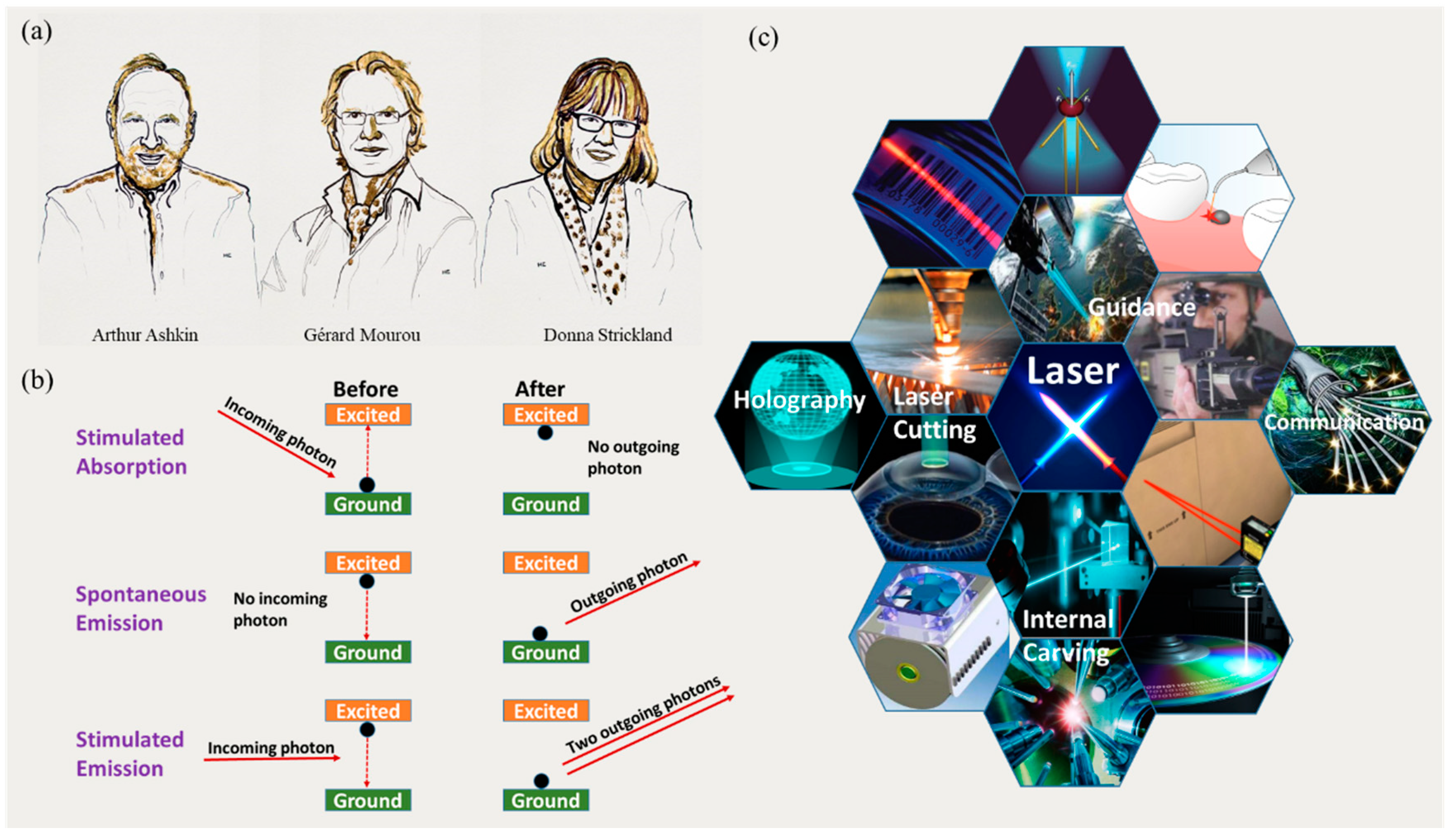
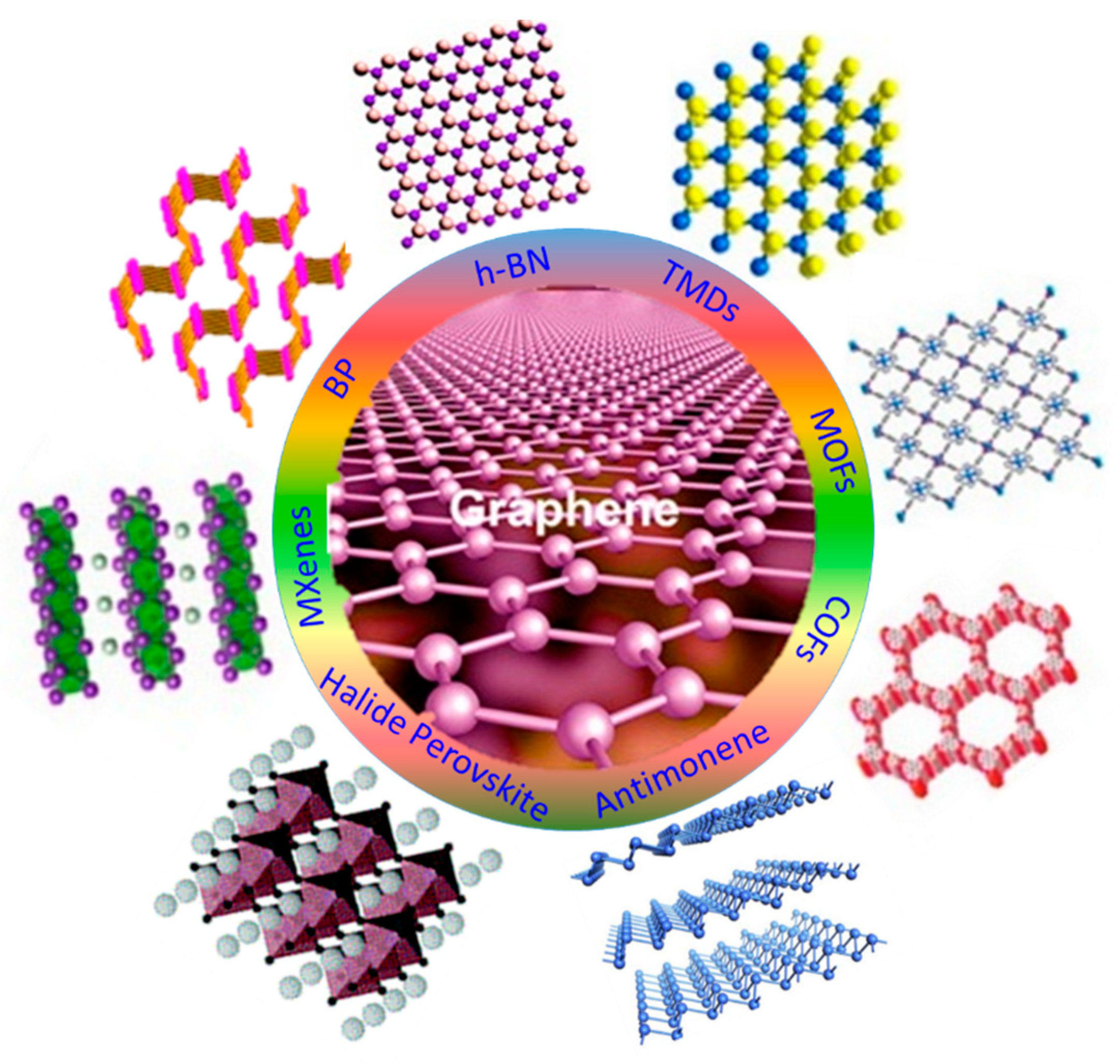
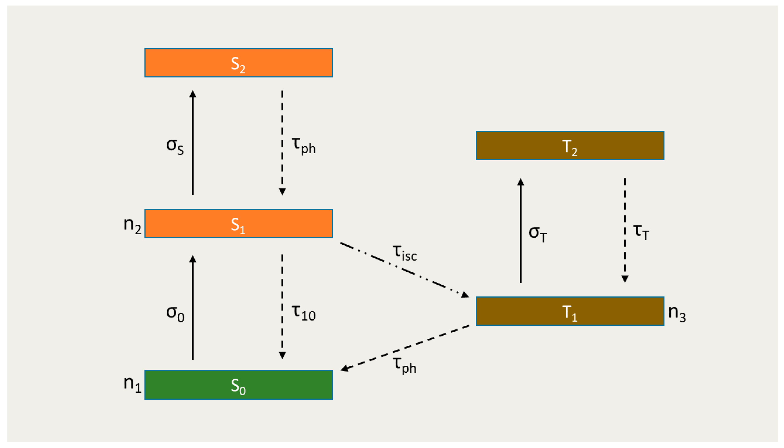
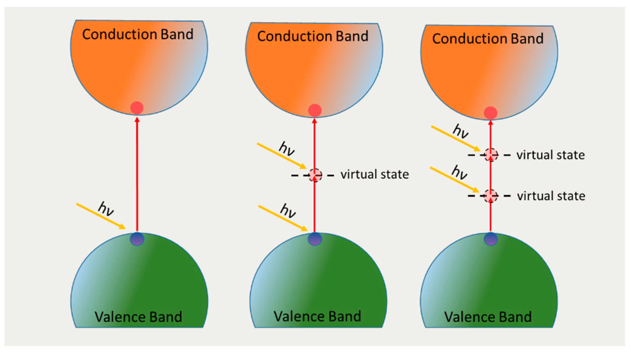
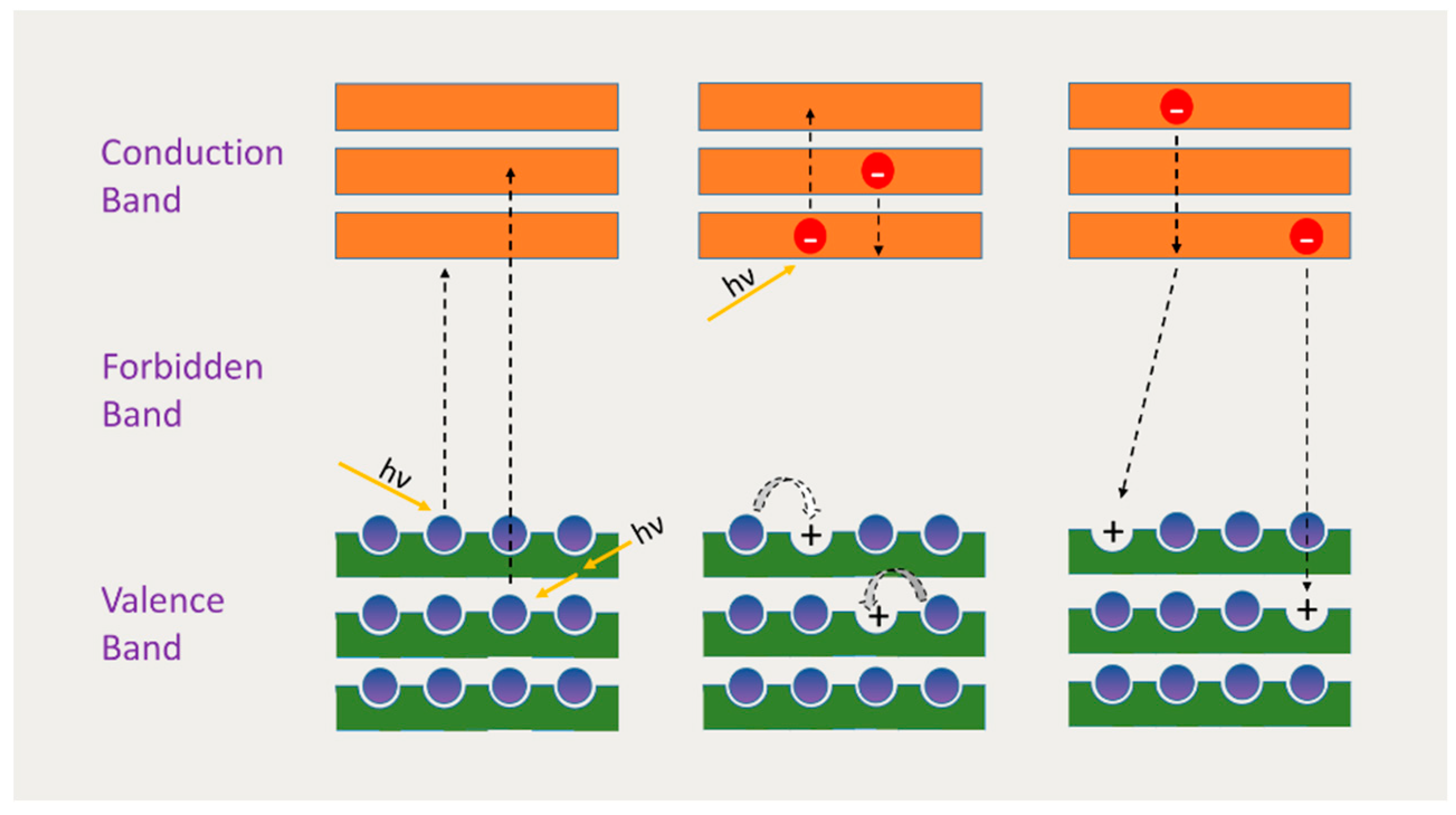
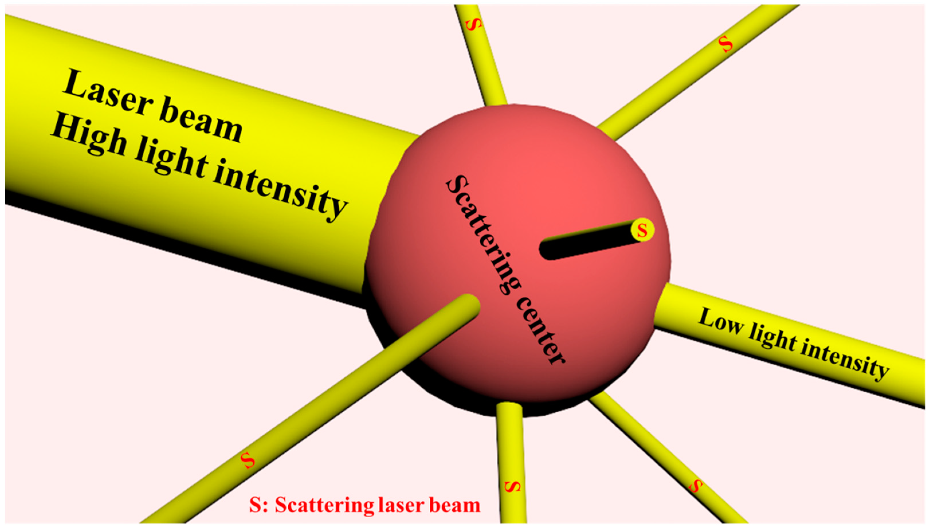
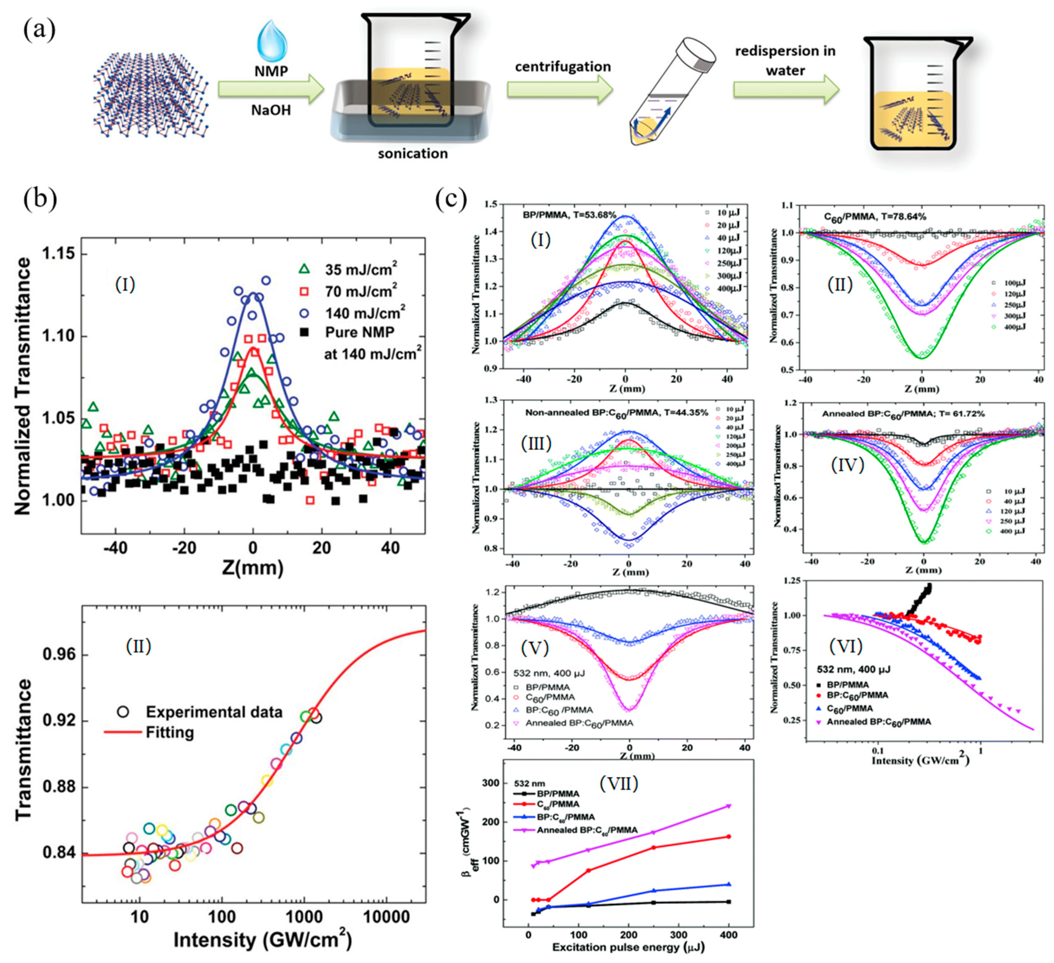
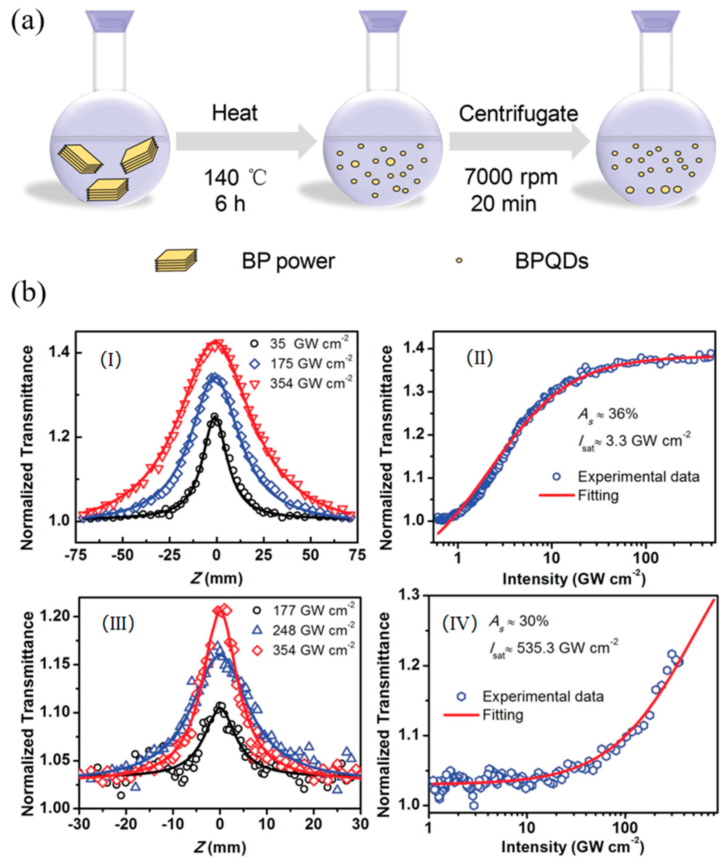
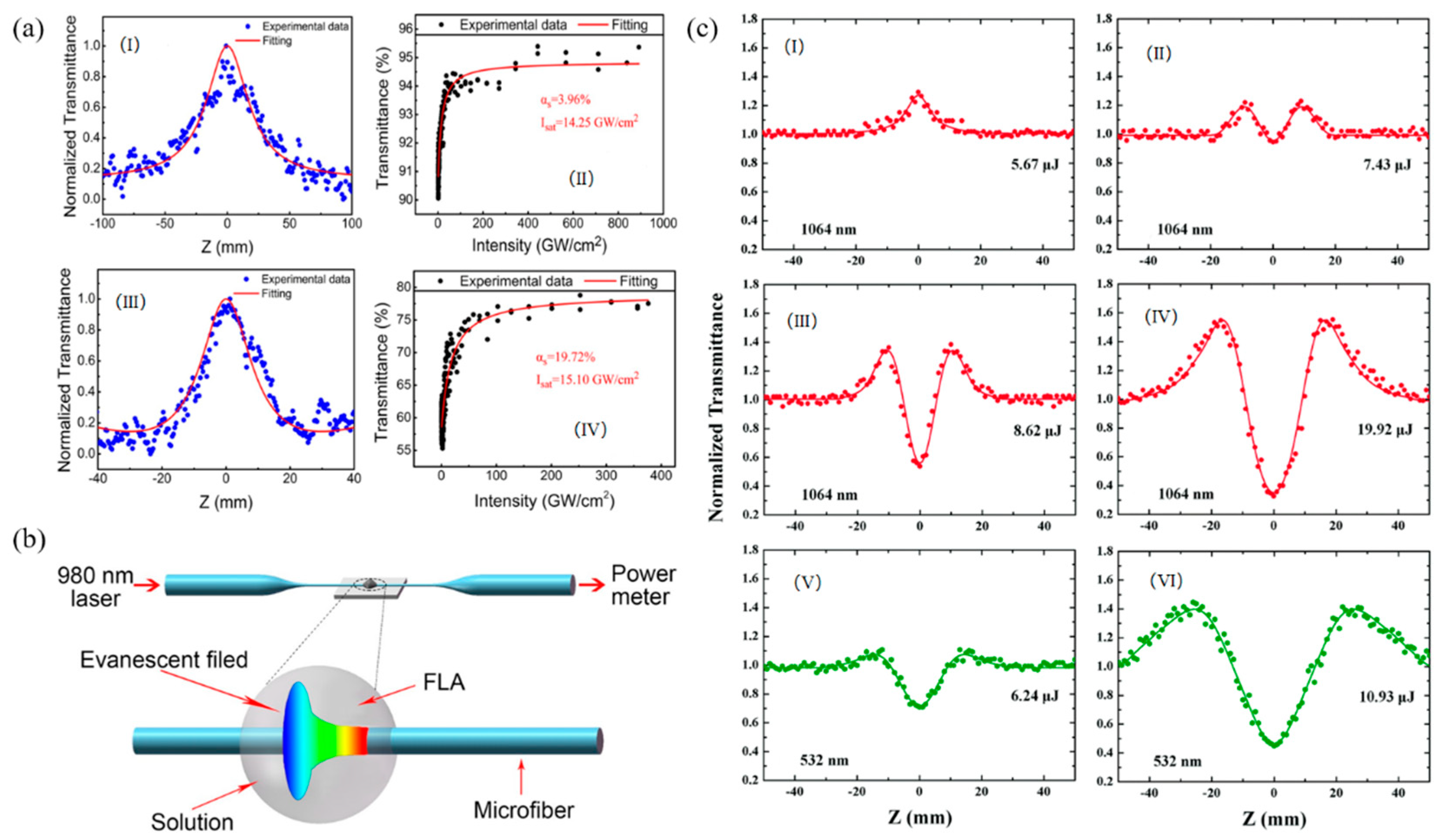
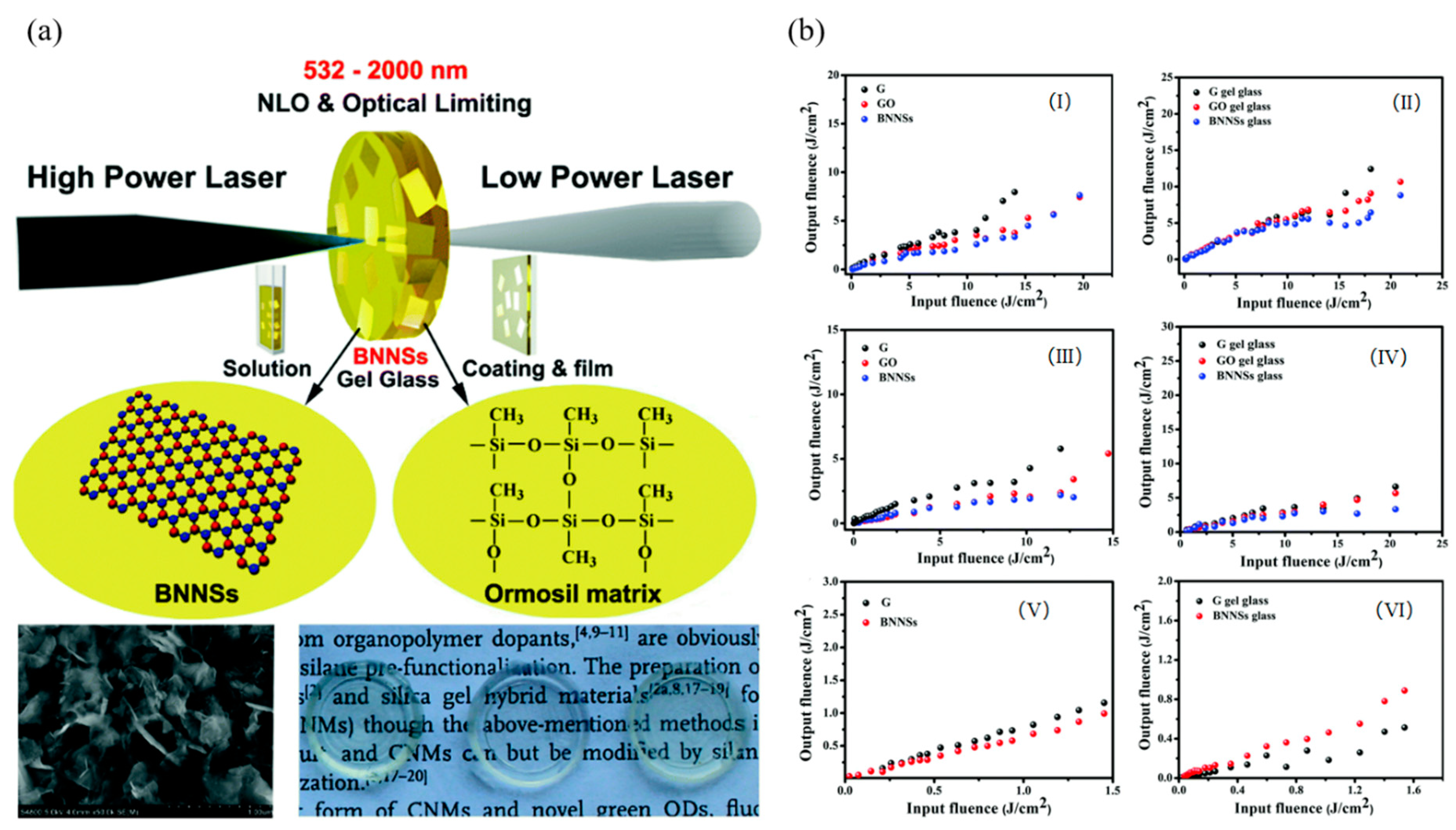
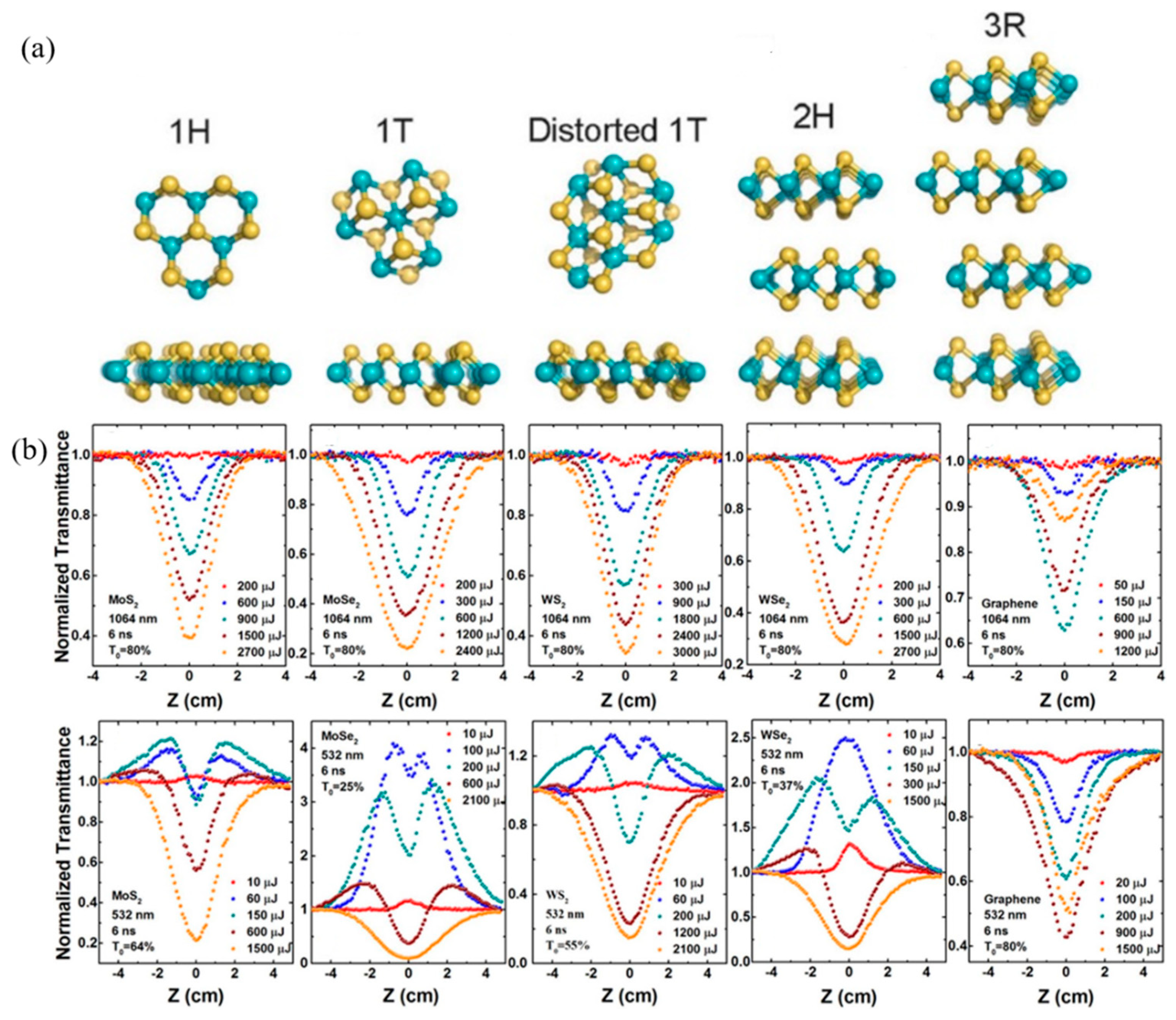
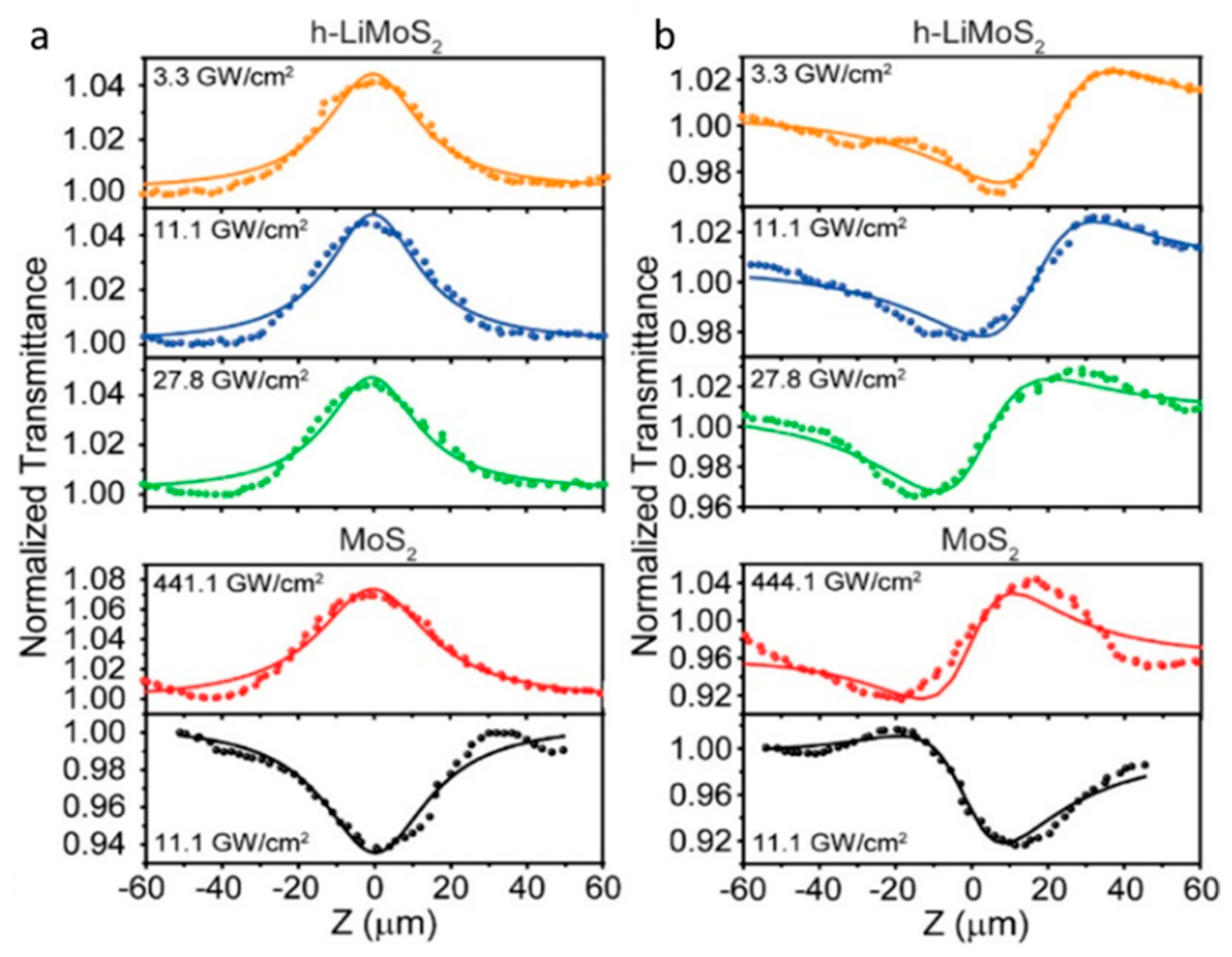
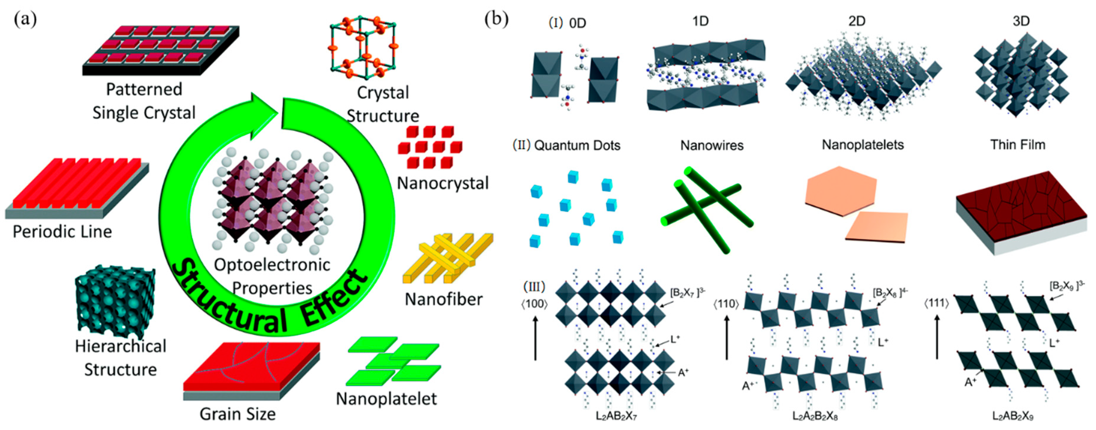
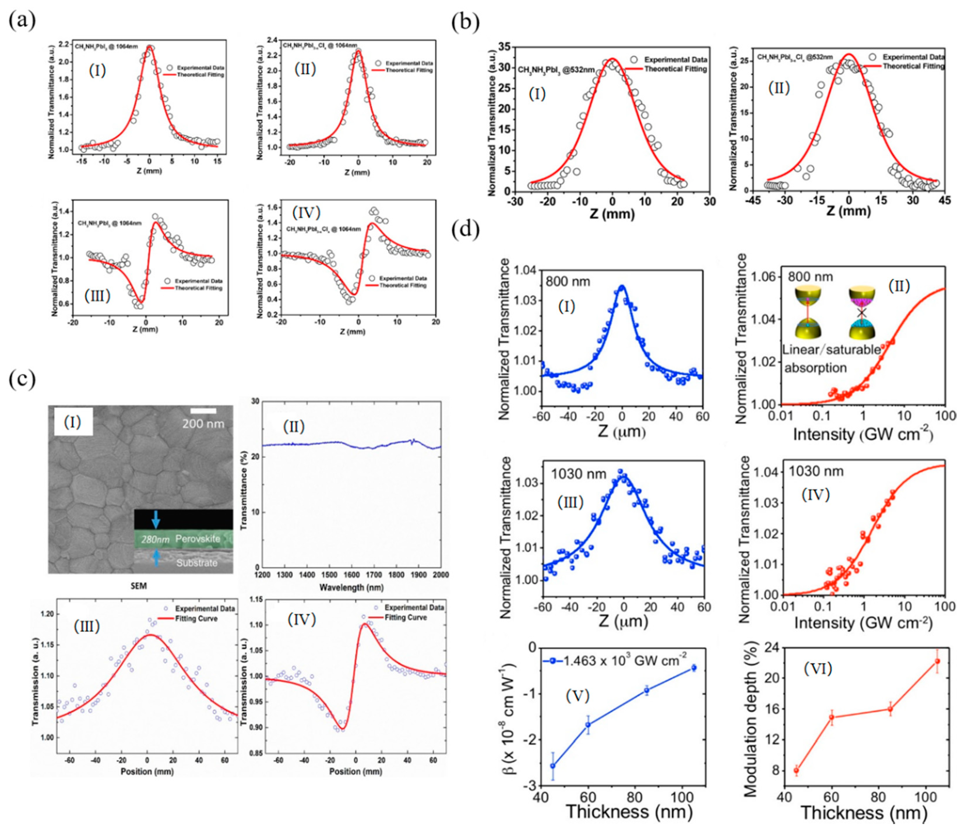
Table 1.
Pathological effects caused by lasers at different wavelengths.
| Wavelength Range | Energy (J) × 10−19 | Pathological Effect |
|---|---|---|
| 180–400 nm (UV) | 4.95–9.90 | Photochemical cataract and keratitis |
| 400–780 nm (visible light) | 2.54–4.95 | Retinal photochemical damage or burn |
| 780–1400 nm (near IR) | 1.40–2.54 | Cataract or retinal burns |
© 2019 by the authors. Licensee MDPI, Basel, Switzerland. This article is an open access article distributed under the terms and conditions of the Creative Commons Attribution (CC BY) license (http://creativecommons.org/licenses/by/4.0/).
Share and Cite
MDPI and ACS Style
Liu, Z.; Zhang, B.; Chen, Y. Recent Progress in Two-Dimensional Nanomaterials for Laser Protection. Chemistry 2019, 1, 17-43. https://doi.org/10.3390/chemistry1010004
AMA Style
Liu Z, Zhang B, Chen Y. Recent Progress in Two-Dimensional Nanomaterials for Laser Protection. Chemistry. 2019; 1(1):17-43. https://doi.org/10.3390/chemistry1010004
Chicago/Turabian StyleLiu, Zhiwei, Bin Zhang, and Yu Chen. 2019. "Recent Progress in Two-Dimensional Nanomaterials for Laser Protection" Chemistry 1, no. 1: 17-43. https://doi.org/10.3390/chemistry1010004