Evanescent Waveguide Sensor for On-Chip Biomolecular Detection †


Department of Information Engineering, Electronics and Telecommunications, Sapienza University of Rome, Rome, Italy
*
Author to whom correspondence should be addressed.
†
Presented at the Eurosensors 2017 Conference, Paris, France, 3–6 September 2017.
Proceedings 2017, 1(4), 562; https://doi.org/10.3390/proceedings1040562
Published: 30 August 2017
(This article belongs to the Proceedings of Proceedings of Eurosensors 2017, Paris, France, 3–6 September 2017)
Abstract
:This work presents analysis and development of an evanescent waveguide sensor system, which integrates an amorphous silicon photodiode and a glass-diffused waveguide. Design of the system includes a study of thickness and refractive index of the transparent electrode of the diode, which are crucial parameters for the optimization of the optical coupling between the waveguide and the photodetector. Preliminary electro-optical measurements on the fabricated device show excellent system performances, and suggest its use for on-chip detection in lab-on-chip applications.
1. Introduction
A Lab-on-Chip (LoC) is a miniaturized system able to integrate several laboratory functions on a single device [1] reducing reagents’ consumption, accelerating detection times, improving sensitivity, miniaturizing size, allowing on-field use and avoiding the presence of specialized personnel [2,3].
These systems analyze biological samples through different process steps: injection, reaction, separation and detection. Among the biological detection techniques, the ones showing the best performances in terms of sensitivity and reliability are those based on the measurements of the optical properties of the analyzed substance, such as absorption, fluorescence or refractive index [4,5].
In some case sample detection is performed measuring, through an off-chip crystalline silicon photo-detector, the effect of the biological analyte on the light propagation in a waveguiding structure [6,7].
This work presents an integrated optoelectronic device based on a glass-diffused waveguide optically coupled with a hydrogenated amorphous silicon (a-Si:H) photosensor, with the purpose of achieving “on-chip” measurement of the light power flowing in the waveguide. This new detector structure, replacing the off-chip optics and detection equipment, allows biomolecular analysis with a more compact and easy-to-use system, with lower cost of analysis.
2. Device Design
2.1. System Structure
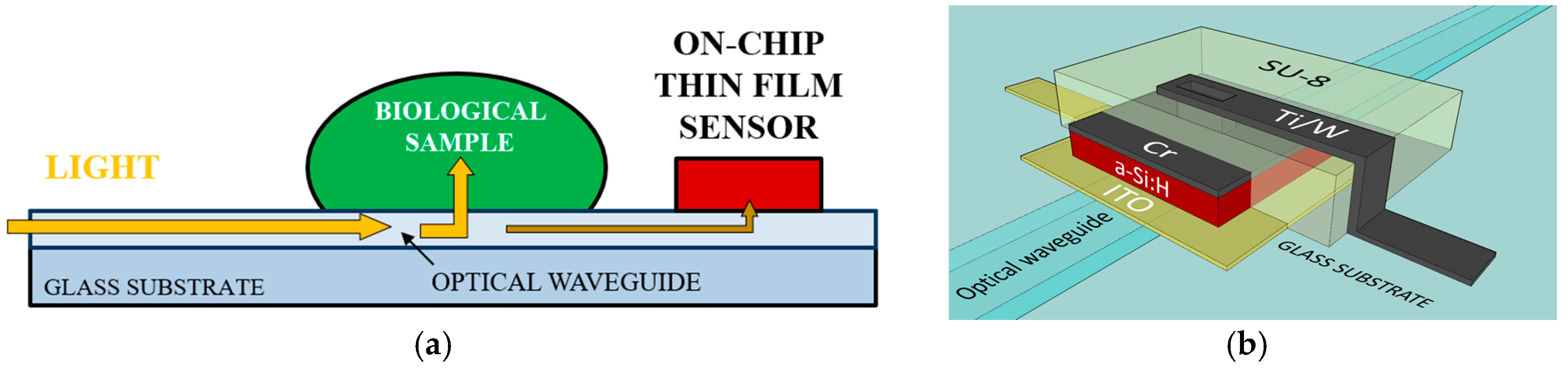
Figure 1a shows the basic structure of the proposed system. A solution containing the analyte is placed in contact with the diffused optical waveguide. A variation in the refractive index of the biological solution, related to the type and concentration of the analyte [8], results in a variation of the intensity of the waveguided light. The thin film sensor, optically coupled to the waveguide, gives a photocurrent signal related to the presence and concentration of the analyte.
The developed system integrates on the same glass substrate two main components: a channel optical waveguide and a photosensor.
Figure 1b reports the three-dimensional sketch of the fabricated device.
Optical waveguides can be made with different processes and materials. Ion-exchanged glass waveguides technology can be used to fabricate simple and low cost optoelectronic devices [9,10,11]. We selected a double ion-exchanged (K+/Ag+ and K+/Na+) thermally annealed channel waveguide diffused on the surface of a borosilicate BK7 glass substrate [12,13]. Our choice opted as project guideline for low propagation losses from visible to infrared spectrum [14].
The photodetector is a thin-film a-Si:H p-doped/intrinsic/n-doped stacked junction. The optoelectronic characteristics of the a-Si:H make this material one of the most promising for the fabrication of thin film devices both in large area electronics [15] and in sensor applications [16,17]. In particular, the low deposition temperature of a-Si:H (below 250 °C) allows the use of different substrates, making it a valuable material for biomolecular recognition applications in compact integrated systems, with performances comparable to those of the c-Si photodiodes [18].
Transparent and conductive indium tin oxide (ITO) layer has been used as bottom contact of the P-I-N junction, to allow the connection of the photodiode to the electronic circuit and the transit of light from the waveguide to the sensor. The top metal is 50 nm-thick chromium layer, which acts both as electrode and as reflector. A 200 nm-thick Ti-W film connects the top electrode to the electronics.
2.2. Simulation Results
The performances of the designed device have been optimized evaluating its coupling efficiency as a ratio between the optical power flux through the waveguide after and before the ITO/P-I-N stacked structure. The whole numerical analysis was carried out using COMSOL Multiphysics at the wavelength of 532 nm, which is within the typical biomolecular emission spectrum [19]. We assumed a 630 nm-thick a-Si:H diode with a refractive index of 4.45. Furthermore we considered refractive indexes of 1.52 for the BK7 substrate and of 1.88 for the ITO film. A waveguide core going 1.5 μm deep into the glass surface with an index variation of 0.04 with respect to the glass substrate index was used. A 50 nm thick top contact chromium layer with a refractive index of 2.66 and 5 µm of SU-8 insulation layer with refractive index of 1.585 was assumed.
We found that, due to its high refractive index, the SU-8 layer absorbs most of the optical power routed into the waveguide before it’s coupled into the photodetector. For this reason, we designed a P-I-N junction electrically insulated on three sides, that receives light from its non-insulated side (see Figure 1b).
A critical point in achieving an optimized coupling efficiency is the thickness of ITO film: variations of this parameter from 25 nm to 700 nm show a cyclic behavior, with optical coupling peaks over 99% at the thicknesses of 120 nm, 375 nm and 625 nm. The lowest values of coupling efficiency (under 60%) occurs at ITO thicknesses equal to 45 nm, 250 nm and 500 nm. For the fabrication phase, we chose a thickness of 120 nm as the best scenario in terms of optical coupling and electrical conductivity in order to guarantee an optimized limit of detection.
3. Device Fabrication and Characterization
3.1. Fabrication Steps
The fabrication process required five photolithographic masks: one for the waveguide geometry definition and four for the a.Si:H photosensor. However we chose to add a mask for the preliminary definition of permanent glass-etched markers, because the standard metal markers are not compatible with the high temperatures reached during the waveguide fabrication processes. The entire fabrication procedure is described in detail in [20].
3.2. Experimental Results
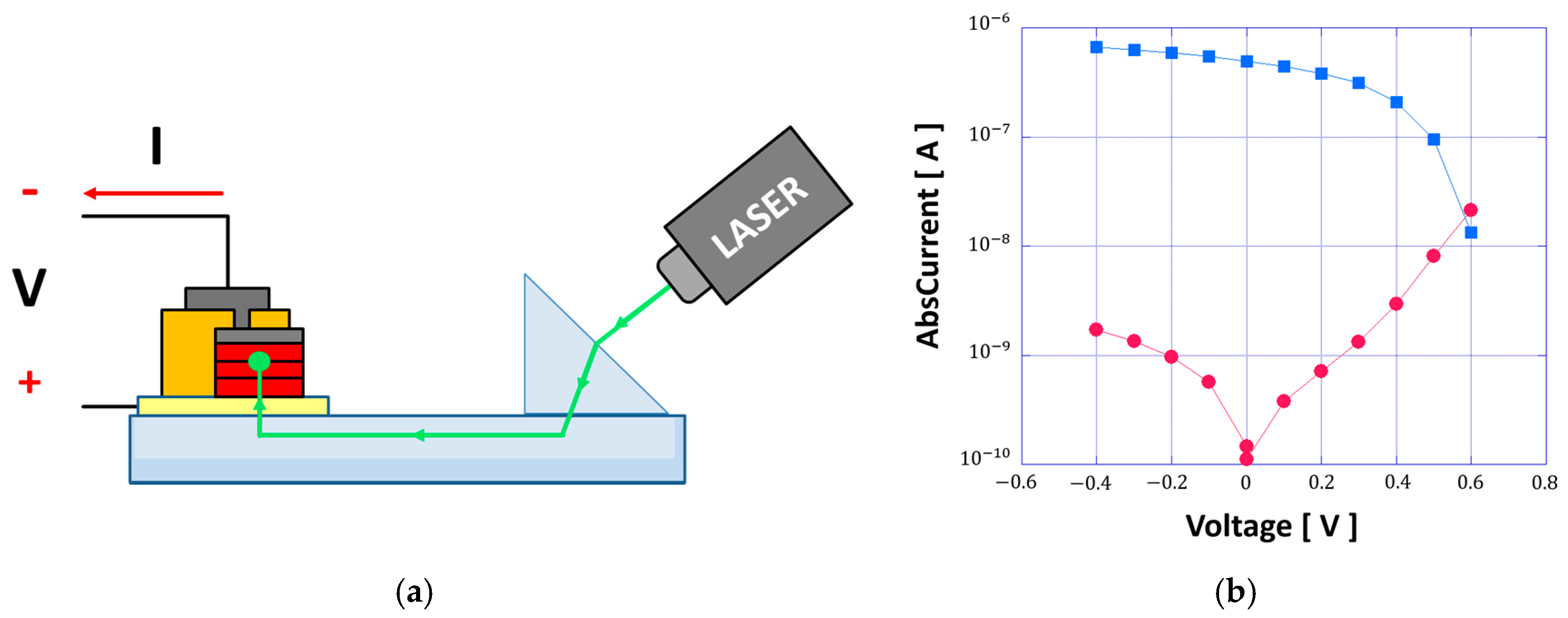
In a first preliminary characterization, we measured the current-voltage characteristics (I–V) of the diode in dark conditions. The reverse saturation current at 100 mV was below 10−11 A, which corresponds to a shot noise level lower than 2 fA. Furthermore, the propagation losses measured in a waveguide before the a-Si:H diode deposition resulted to be around 2 dB/cm.
Figure 2a reports the schematic measurement setup. A 532 nm laser light source is coupled through a prism to the optical waveguide. A Source Measure Unit (SMU) Keithley 236 is used to read the sensor photocurrent. Figure 2b shows the current-voltage curve of the photosensor obtained with and without 15 μW optical power in the waveguide.
We see that, in the operating range voltages of the photodiode (small reverse bias), the presence of the laser beam induces a variation of the photocurrent of about three orders of magnitude, demonstrating the successful on-chip detection of light propagating in a waveguide by a thin film a-Si:H photosensor.
4. Conclusions
This work reports the design, fabrication and preliminary characterization of an integrated evanescent waveguide sensor system based on an amorphous silicon photodiode and an ion-exchanged glass-diffused waveguide. We studied the behavior of the two components and their optical coupling, providing their successful integration on the same glass substrate. Currently, works are in progress to accomplish a quantitative characterization of the system. Taking into account the presented results, our structure is a promising candidate in smart and high-sensitive systems for on-chip recognition of biomolecules.
Acknowledgments
Authors would like to thank the Center for Life Nano Scienze Sapienza, Istituto Italiano di Tecnologia (Rome, Italy) and the University Research Project 2015 (prot. C26H15J3PX) for the financial supports.
Conflicts of Interest
The authors declare no conflict of interest.
References
- Caputo, D.; Ceccarelli, M.; de Cesare, G.; Nascetti, A.; Scipinotti, R. Lab-on-glass system for DNA analysis using thin and thick film technologies. Mater. Res. Soc. Symp. Proc. 2009, 1191, 53–58. [Google Scholar] [CrossRef]
- Jung, W.E.; Han, J.; Choi, J.-W.; Ahn, C.H. Point-of-care testing (POCT) diagnostic systems using microfluidic lab-on-a-chip technologies. Microelectron. Eng. 2015, 132, 46–57. [Google Scholar] [CrossRef]
- De Venuto, D.; Carrara, S.; Riccò, B. Design of an integrated low-noise read-out system for DNA capacitive sensors. Microelectron. J. 2009, 40, 1358–1365. [Google Scholar] [CrossRef]
- Costantini, F.; Nascetti, A.; Scipinotti, R.; Domenici, F.; Sennato, S.; Gazza, L.; Bordi, F.; Pogna, N.; Manetti, C.; Caputo, D.; et al. On-chip detection of multiple serum antibodies against epitopes of celiac disease by an array of amorphous silicon sensors. RSC Adv. 2014, 4, 2073–2080. [Google Scholar] [CrossRef]
- Fixe, F.; Chu, V.; Prazeres, D.M.F.; Conde, J.P. An on-chip thin film photodetector for the quantification of DNA probes and targets in microarrays. Nucleic Acids Res. 2004, 32, e70–e75. [Google Scholar] [CrossRef] [PubMed]
- Estevez, M.C.; Alvarez, M.; Lechuga, L.M. Integrated optical devices for lab-on-a-chip bio-sensing applications. Laser Photon. 2012, 6, 463–487. [Google Scholar] [CrossRef]
- Schmitta, K.; Schirmera, B.; Hoffmanna, C.; Brandenburga, A.; Meyrueisb, P. Interferometric biosensor based on planar optical waveguide sensor chips for label-free detection of surface bound bioreactions. Biosens. Bioelectron. 2007, 22, 2591–2597. [Google Scholar] [CrossRef] [PubMed]
- Jin, Y.L.; Chen, J.Y.; Xu, L.; Wang, P.N. Refractive index measurement for biomaterial samples by total internal reflection. Phys. Med. Biol. 2006, 51, N371–N379. [Google Scholar] [CrossRef] [PubMed]
- Asquini, R.; d’Alessandro, A. Tunable photonic devices based on liquid crystals and composites. In Liquid Crystals XVII, Proceedings of the SPIE Optics + Photonics, Organic Photonics and Electronics, San Diego, CA, USA, 25–29 August 2013; International Society for Optics and Photonics: San Diego, CA, USA, 2013; Volume 8828, p. 88280T. [Google Scholar]
- Gizzi, C.; Asquini, R.; d’Alessandro, A. A polarization independent liquid crystal assisted vertical coupler switch. Mol. Cryst. Liq. Cryst. 2004, 421, 95–105. [Google Scholar] [CrossRef]
- Gilardi, G.; Asquini, R.; d’Alessandro, A.; Beccherelli, R.; De Sio, L.; Umeton, C. All-optical and thermal tuning of a Bragg grating based on photosensitive composite structures containing liquid crystals. Mol. Cryst. Liq. Cryst. 2012, 558, 64–71. [Google Scholar] [CrossRef]
- Zou, J.; Zhao, F.; Chen, R.T. Two-step K+–Na+ and Ag+–Na+ ion-exchanged glass waveguides for C-band applications. Appl. Opt. 2002, 41, 7620–7626. [Google Scholar] [CrossRef] [PubMed]
- Gizzi, C.; Asquini, R.; d’Alessandro, A. An integrated 2 × 2 SSFLC optical switch with channel ion exchanged glass waveguides. Ferroelectrics 2004, 312, 31–37. [Google Scholar] [CrossRef]
- Asquini, R.; d’Alessandro, A. Bistable optical waveguided switch using a ferroelectric liquid crystal layer. In Proceedings of the 13th IEEE Annual Meeting Lasers and Electro-Optics Society 2000 Annual Meeting (LEOS 2000), Rio Grande, Puerto Rico, USA, 13–16 November 2000; Volume 1, pp. 119–120. [Google Scholar]
- Caputo, D.; de Cesare, G. New a-Si:H two terminal switching device for active display. J. Non-Cryst. Solids 1996, 198–200, 1134–1136. [Google Scholar] [CrossRef]
- De Cesare, G.; Palma, F.; Gavesi, M.; Riccò, B. A novel a-Si:H mechanical stress sensor. Thin Solid Films 2003, 427, 191–195. [Google Scholar] [CrossRef]
- Knipp, D.; Herzog, P.G.; Stiebig, H. Stacked amorphous silicon color sensors. IEEE Trans. Electron. Devices 2002, 49, 170–176. [Google Scholar] [CrossRef]
- Zangheri, M.; Di Nardo, F.; Mirasoli, M.; Anfossi, L.; Nascetti, A.; Caputo, D.; de Cesare, G.; Guardigli, M.; Roda, A. Chemiluminescence lateral flow immunoassay cartridge with integrated amorphous silicon photosensors array for human serum albumin detection in urine samples. Anal. Bioanal. Chem. 2016, 408, 8869–8879. [Google Scholar] [CrossRef] [PubMed]
- Caputo, D.; de Cesare, G.; Scipinotti, R.; Stasio, N.; Costantini, F.; Manetti, C.; Nascetti, A. On-chip diagnosis of celiac disease by an amorphous silicon chemiluminescence detector. Lect. Notes Electr. Eng. 2014, 268, 183–187. [Google Scholar]
- De Cesare, G.; Asquini, R.; Buzzin, A.; Caputo, D. Electro-optical detector for lab-on-chip applications. In Proceedings of the 7th IEEE International Workshop on Advances in Sensors and Interfaces (IWASI), Vieste, Italy, 15–16 June 2017; pp. 203–206. [Google Scholar]
Figure 1.
(a) Basic structure of the proposed system; (b) Three-dimensional sketch of the fabricated device.
Figure 1.
(a) Basic structure of the proposed system; (b) Three-dimensional sketch of the fabricated device.

Figure 2.
(a) Schematic measurement setup with a 532 nm laser; (b) Current-voltage characteristics of the photodiode with (blue squares) and without (red circles) laser beam routed into the waveguide.
Figure 2.
(a) Schematic measurement setup with a 532 nm laser; (b) Current-voltage characteristics of the photodiode with (blue squares) and without (red circles) laser beam routed into the waveguide.

Publisher’s Note: MDPI stays neutral with regard to jurisdictional claims in published maps and institutional affiliations. |
© 2017 by the authors. Licensee MDPI, Basel, Switzerland. This article is an open access article distributed under the terms and conditions of the Creative Commons Attribution (CC BY) license (https://creativecommons.org/licenses/by/4.0/).
Share and Cite
MDPI and ACS Style
Cesare, G.d.; Asquini, R.; Buzzin, A.; Caputo, D. Evanescent Waveguide Sensor for On-Chip Biomolecular Detection. Proceedings 2017, 1, 562. https://doi.org/10.3390/proceedings1040562
AMA Style
Cesare Gd, Asquini R, Buzzin A, Caputo D. Evanescent Waveguide Sensor for On-Chip Biomolecular Detection. Proceedings. 2017; 1(4):562. https://doi.org/10.3390/proceedings1040562
Chicago/Turabian StyleCesare, Giampiero de, Rita Asquini, Alessio Buzzin, and Domenico Caputo. 2017. "Evanescent Waveguide Sensor for On-Chip Biomolecular Detection" Proceedings 1, no. 4: 562. https://doi.org/10.3390/proceedings1040562