Proceeding Paper

Multimodal Neuroimaging Microtool for Infrared Optical Stimulation, Thermal Measurements and Recording of Neuronal Activity in the Deep Tissue
 †

1
MTA EK NAP B Research Group for Implantable Microsystems, Budapest, Hungary
2
Doctoral School of Material Science & Technology, Óbuda University, Budapest, Hungary
3
Department of Atomic Physics, Budapest University of Technology & Economics, Budapest, Hungary
*
Author to whom correspondence should be addressed.
Presented at the Eurosensors 2017 Conference, Paris, France, 3–6 September 2017.
Proceedings 2017, 1(4), 494; https://doi.org/10.3390/proceedings1040494
Published: 25 August 2017
(This article belongs to the Proceedings of Proceedings of Eurosensors 2017, Paris, France, 3–6 September 2017)

Abstract

:
Infrared neural stimulation (INS) uses pulsed near-infrared light to generate highly controlled temperature transients in neurons, leading them to fire action potentials. Stimulation of the superficial layer of the intact brain has been presented, however, the stimulation of the deep neural tissue has larger potential in view of therapeutic use. To reveal the underlying mechanism of deep tissue stimulation properly, we present the design, the fabrication scheme and functional testing of a novel, multimodal microelectrode for future INS experiments. Three modalities—electrophysiological recording, thermal measurements and infrared waveguiding abil—were integrated based on silicon MEMS technology. Due to the advanced functionalities, a single probe is sufficient to determine safe stimulation parameters in vivo. As far as we know, this is the first multimodal microelectrode designed for INS studies in deep neural tissue. In this paper, the technology and results of chip-scale measurements are presented.

1. Introduction

Infrared neural stimulation (INS) is an emerging method, first presented by Wells et al. in 2005 [1]. Spatially controlled short pulses of infrared light are used to modulate neuronal activity without molecular intervention or sensitization. Recent tools to deliver infrared radiation are limited to the stimulation of the cortical surface of animal models, however, the technological advances of silicon microelectrode fabrication open doors to new opportunities in the integration of several functionalities in a single device. In this work, we present the development of a multimodal, single crystalline silicon-based neural microelectrode for INS in the deep tissue. In our system, silicon has both mechanical and optical functionality provided by post-processing steps based on the combined use of wet chemicals [2]. These type of multimodal brain electrodes provide a less invasive way of deep tissue infrared neural stimulation in combination with recording neuronal activity and local temperature changes in the close vicinity of the stimulation site.

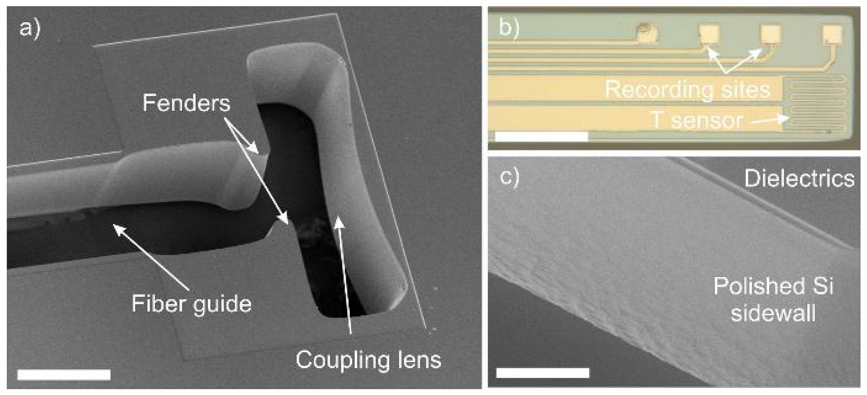
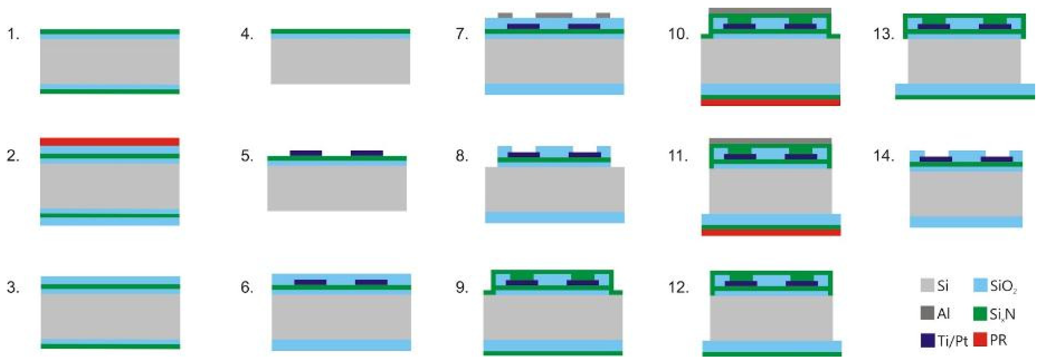
2. Design and Technology

Integrated modalities make the microelectrode able to locally modify the temperature of neural tissue, while the evoked neural response can be recorded from the closest vicinity. Thermal modulation is realized via IR irradiation. in our case, the bulk Si is not only utilized as a mechanical carrier of the electrical recording sites, but also as an IR waveguide. Integrated coupling lens and a low-loss waveguiding shaft (see Figure 1a,c) can deliver the IR light from light source to deep brain regions. Electrophysiological recording sites and integrated resistance thermometer are made of sputtered Ti/Pt patterned by lift-off process and sandwiched between SiO2/SiN dielectric stacks. They are positioned close to the stimulation site which provides true local information on evoked neural activity and on accumulated heat. To ease the evaluation of bench top tests through measurement with a CMOS beam profiler, we designed blunt tip probes (Figure 1b).
On Figure 2, the schematic of our Si-based MEMS manufacturing process supplemented additional wet etching steps at the back-end are shown. Our proposed technology reduces the surface roughness of the optrode’s sidewall what is caused by the electrode shape release technique, deep reactive ion etching (DRIE). The aim of it is to increase IR light coupling efficiency.

3. Test Methods

In this section, we present preliminary, bench top measurements on each modality, including a short description, and characteristic parameters summarized in Table 1.

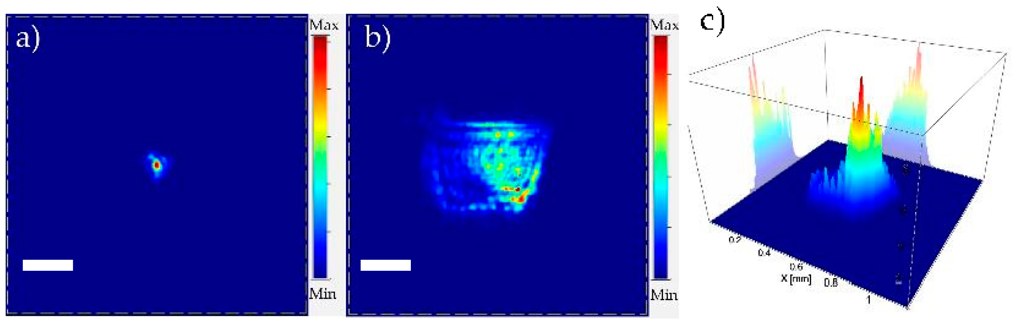
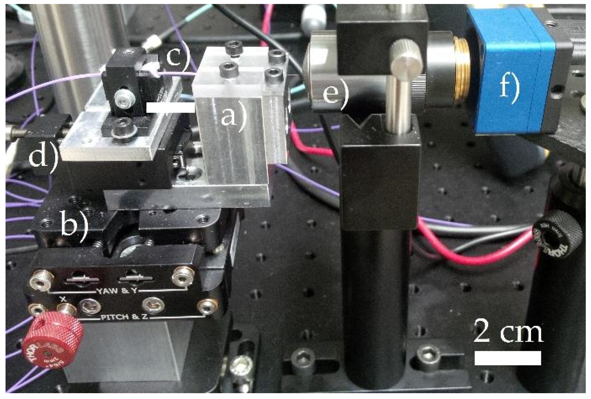
3.1. Optical Characterization

The waveguiding ability of individual chips was tested via relative LASER beam power measurement. On Figure 3, a representative measured IR beam profile is shown. First, the light (λ = 1310 nm) emitted from the optical fibre was measured (a), then the fibre was inserted into the chip’s fibre guide and the light from the optrode’s tip was measured again (b). The ratio of these beam powers are considered as, the overall coupling efficiency of our system. Figure 4 shows the setup of optical characterization.

3.2. Thermal Characterization

Each optrode chip contains a meander-shape platinum resistance thermometer positioned as close as possible to the recording sites as Figure 1b shows. They were calibrated with a negative temperature coefficient (NTC) thermistor (ΔT = ±0.14 °C, Semitec 223Fμ5183-15U004, Mouser Electronics) [3]. At body temperature (34–39 °C), the Callendar–Van Dusen equation is linear: Rt = R0 [1 + α · ΔT]. The parameters in our case are listed in Table 1. The resistance of the temperature sensing filament is measured by four-wire setup with 1 mA measuring current (Keithley 2000 multimeter and Keithley 6221 current source). Utilizing the optrode’s waveguiding modality, IR irradiation may cause considerable temperature rise in the close vicinity of the optrode in the brain tissue. Therefore, the monitoring of accumulated heat by the integrated sensor is important in view of possible tissue damages. The cooperative functioning of these two modalities may be further exploited to control the local tissue temperature.

3.3. Electrical Characterization

Potentiostatic electrochemical impedance spectroscopy (EIS) was used to validate the rectangular platinum recording sites (Reference 600, Gamry Instruments, Warminster, PA, USA). The electrolyte solution is phosphate buffered saline (PBS), the reference is a silver/silver-chloride electrode always maintained at a constant potential, each Pt recording sites are connected to the working electrode pin, and the counter electrode is a Pt wire as well. During the measurement process, the voltage between a recording site and the reference electrode induces charger transport between itself and the counter electrode and this transport can be measured as current. The impedance of the recording sites are of sufficiently low impedance for recording activity of individual neurons.

Acknowledgments

The supportive work of the cleanroom staff of MTA EK MFA in micromachining, and the contribution of A.J.C. in the preparative work on the optical fibers are highly appreciated. The authors are also thankful to the Hungarian Brain Research Program (KTIA NAP 13-2-2015-0004).

Conflicts of Interest

The authors declare no conflict of interest.

References

  1. Wells, J.; Kao, C.; Jansen, E.D.; Konrad, P.; Mahadevan-Jansen, A. Application of infrared light for in vivo neural stimulation. J. Biomed. Opt. 2005, 10, 064003. [Google Scholar] [CrossRef] [PubMed]
  2. Kiss, M.; Földesy, P.; Fekete, Z. Optimization of a Michigan-type silicon microprobe for infrared neural stimulation. Sens. Actuators B Chem. 2016, 224, 676–682. [Google Scholar] [CrossRef]
  3. Fekete, Z.; Csernai, M.; Kocsis, K.; Horváth, Á.C.; Pongrácz, A.; Barthó, P. Simultaneous in vivo recording of local brain temperature and electrophysiological signals with a novel neural probe. J. Neural Eng. 2017, 14, 034001. [Google Scholar] [CrossRef] [PubMed]
Figure 1. Close SEM view of the coupling region on the chip (a). Tip of a fully functional optrode (b). Close microscopy (b) and representative SEM view of the shaft polished sidewall (c). Scale bar shows 100 microns on all figures.
Proceedings 01 00494 g001
Figure 2. Fabrication sequence of INS electrodes. (1) SiO2 and SixNy deposition; (2) LTO deposition and front-side photoresist protection; (3) HF etch and PR removal; (4) Backside nitride and oxide removal; (5) Ti/Pt deposition and lift-off; (6) LTO deposition; (7) Deposition, photolithography and etching of Al mask for DRIE; (8) Dielectric stack removal in DRIE and Al removal in wet etchant; (9) SixNy deposition; (10) Deposition, photolithography and etching of Al mask for DRIE with backside PR protective layer; (11) Deep silicon etching in DRIE; (12) Removal of Al mask and protective PR layer; (13) Wet chemical polishing; (14) HF etch and SixNy removal in phosphoric acid.
Proceedings 01 00494 g002
Figure 3. IR beam profile measured on the end facet of multimode fibre (a) and blunt-tip silicon shaft of a fully functional optrode chip (b). 3D view of the intensity of IR beam profile coupled out from the electrode’s shaft (c). The pixel intensity is in arbitrary units in all figures. Scale bar shows 300 µm on both of Figure 3a,b.
Proceedings 01 00494 g003
Figure 4. Photo of the optical measurement setup: the chip under test is inserted in a custom designed sample holder (a) fastened on a 3D translation stage (b). IR light is delivered via a multimode fibre (c) whose position can be adjusted by a 1D translation stage (d). Imaging optic (e) is a microscope objective (50×, NA = 0.8). All measured data are registered by a CMOS beam profiler (CinCam CMOS Nano, CINOGY Technologies GmbH) (f).
Proceedings 01 00494 g004
Table 1. A summary of the microelectrode’s characteristic parameters.
Parameter (dim.)Value
Shaft width (μm)170
Shaft thickness (μm)190
Shaft length (mm)5
Recording site area (μm2)900
Number of recording sites4–16
Zsite at 1 kHz (kΩ)1031 ± 95
αTsensor (ppm/K)2636 ± 75
Detection limit (°C)0.14
Thermal time constant (ms)472
Waveguide efficiency (%)32.04 ± 4.10

