Proceeding Paper

Incorporation of ZnO Nanostructures in MIS Architecture through Chemical Routes †

by
Rubén J. Aranda García
1,
A. Escobedo Morales
1,
J. Carrillo López
2,
M. Dominguez Jimenez
2,
N. Carlos Ramírez
3 and
José Alberto Luna López
2,*
1
Facultad de Ingeniería Química, Benemérita Universidad Autónoma de Puebla, 5013 Puebla, Pue., Mexico
2
IC-CIDS Benemérita Universidad Autónoma de Puebla, Ed. IC5 o IC6, Col. San Manuel, C.P. 72570 Puebla, Pue., Mexico
3
INAOE, Electronics Department, Apartado 51, 72000 Puebla, Mexico
*
Author to whom correspondence should be addressed.
Presented at the Eurosensors 2017 Conference, Paris, France, 3–6 September 2017.
Proceedings 2017, 1(4), 308; https://doi.org/10.3390/proceedings1040308
Published: 18 August 2017
(This article belongs to the Proceedings of Proceedings of Eurosensors 2017, Paris, France, 3–6 September 2017)

Abstract

:
Because it’s physical properties, ZnO is considered a potential semiconductor compound for fabricating electronic and optoelectronic functional devices. In this regard, several growth techniques have been developed in order to meet the requirements of commercial devices based in this material. On the pathway for improving the performance of the current devices, low-dimensional ZnO structures seem a promising alternative. Here, we report the process to obtain a metal-insulator-semiconductor (MIS) structure based on ZnO nanostructures grown on the surface of an anodized aluminum substrate (Al2O3/Al) by chemical routes.
Keywords:
ZnO; SEM; morphology; XRD; MIS

1. Introduction

Zinc oxide (ZnO) is recognized as one of the most promising semiconductor oxides so research in relation to its electronic and optoelectronic properties has increased substantially in recent years. The main cause of this renewed interest in ZnO is mainly due to two of its characteristics: its direct forbidden gap of 3.37 eV at room temperature and its high exciton bond energy of 60 meV. These characteristics make it a potential material for the manufacture of electronic and optoelectronic devices that work in the ultraviolet range at room temperature and with good stability. In addition, the presence of deep levels from the intrinsic and extrinsic defects of the material allows the ZnO nanostructures to exhibit luminescence in the range of blue, green, yellow and orange-red [1,2,3]. Thus, ZnO nanostructures can be formally applied in a wide range of LEDs that can cover a wide range of the visible spectral zone. This material is a promising candidate for the manufacture of white light sources. Due to the possibilities of ZnO in photovoltaic applications and to its great sensitivity to different chemical environments, many other investigations are being oriented towards the technological application of the nanostructures of this material in solar cells and gas sensors. This type of technological applications is of great importance if it is to resolve or reduce some of the environmental problems caused by high energy consumption and emissions of polluting or volatile gases by industries, households and the use of cars.

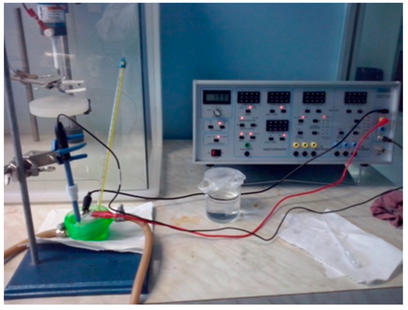
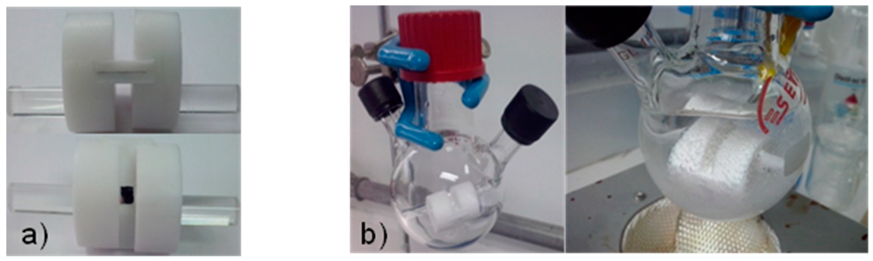
2. Materials and Methods

The fabrication of the MIS structure (ZnO/Al2O3/Al) consisted basically of 4 steps which are described below: (1) cleaning the Al substrate; (2) electropolishing process; (3) anodizing process and (4) growth of ZnO nanostructures. Anodizing process, this process was carried out to form the insulating barrier (Al2O3) on the metallic substrate (Al). For this process, the same materials used in the electropolishing process were used (Figure 1), except that the electrolytic solution was a mixture of 0.5 M H3BO3 and 0.05 M Na2B4O7, and the temperature was maintained at 20 ± 0.5 °C. Applying a current of 1 mA for 30 s carried out the anodizing process.
The ZnO nanostructures were grown on an anodized aluminum substrate (Al2O3/Al) using the hydrothermal chemical pathway. The growth of ZnO nanostructures was carried out by preparing 70 mL of an equimolar solution (7.5 mM) of Zn(NO3)2·6H2O and hexamethyltetramine3. For the growth of the nanostructures, another Teflon device was designed and machined in order to only contact the anodized surface of the Al substrate with the precursor solution (see Figure 2). The growth process was carried out at 70 ± 1 °C for 2 h. After the reaction time had elapsed, the solution was allowed to cool freely until it reached 25 °C, then the substrate was rinsed with ultra-pure deionized water, finally thermally treated at 300 °C for 2 h in a tubular furnace.

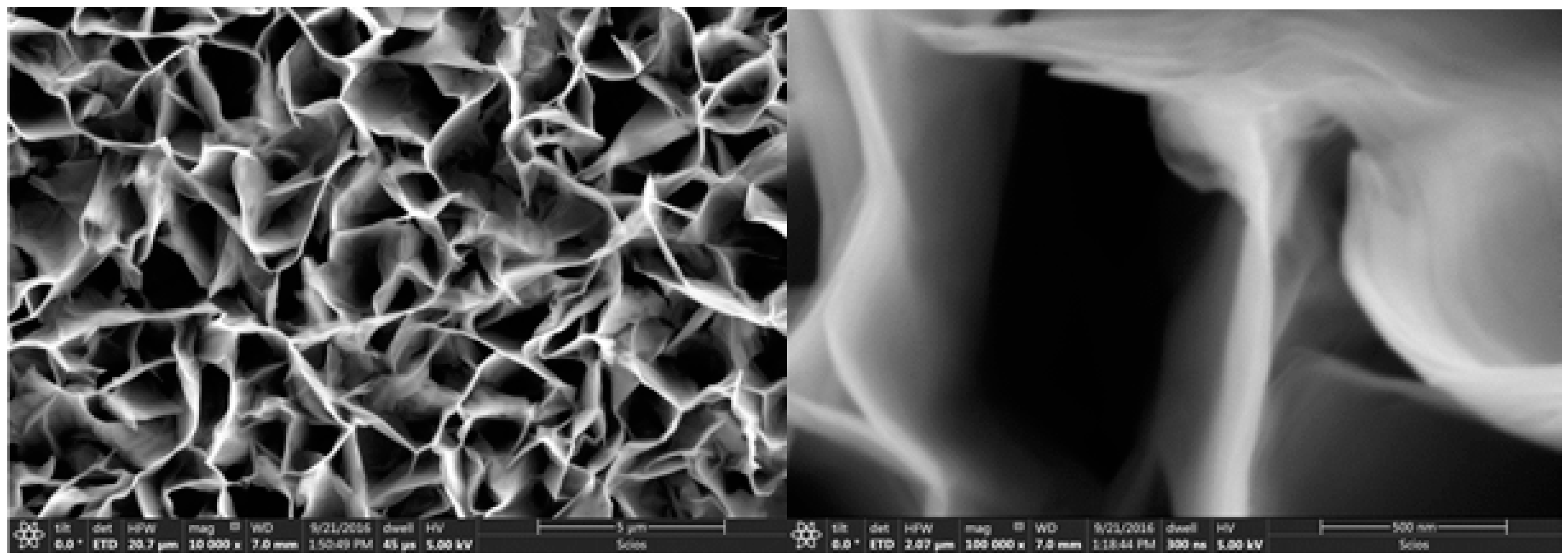
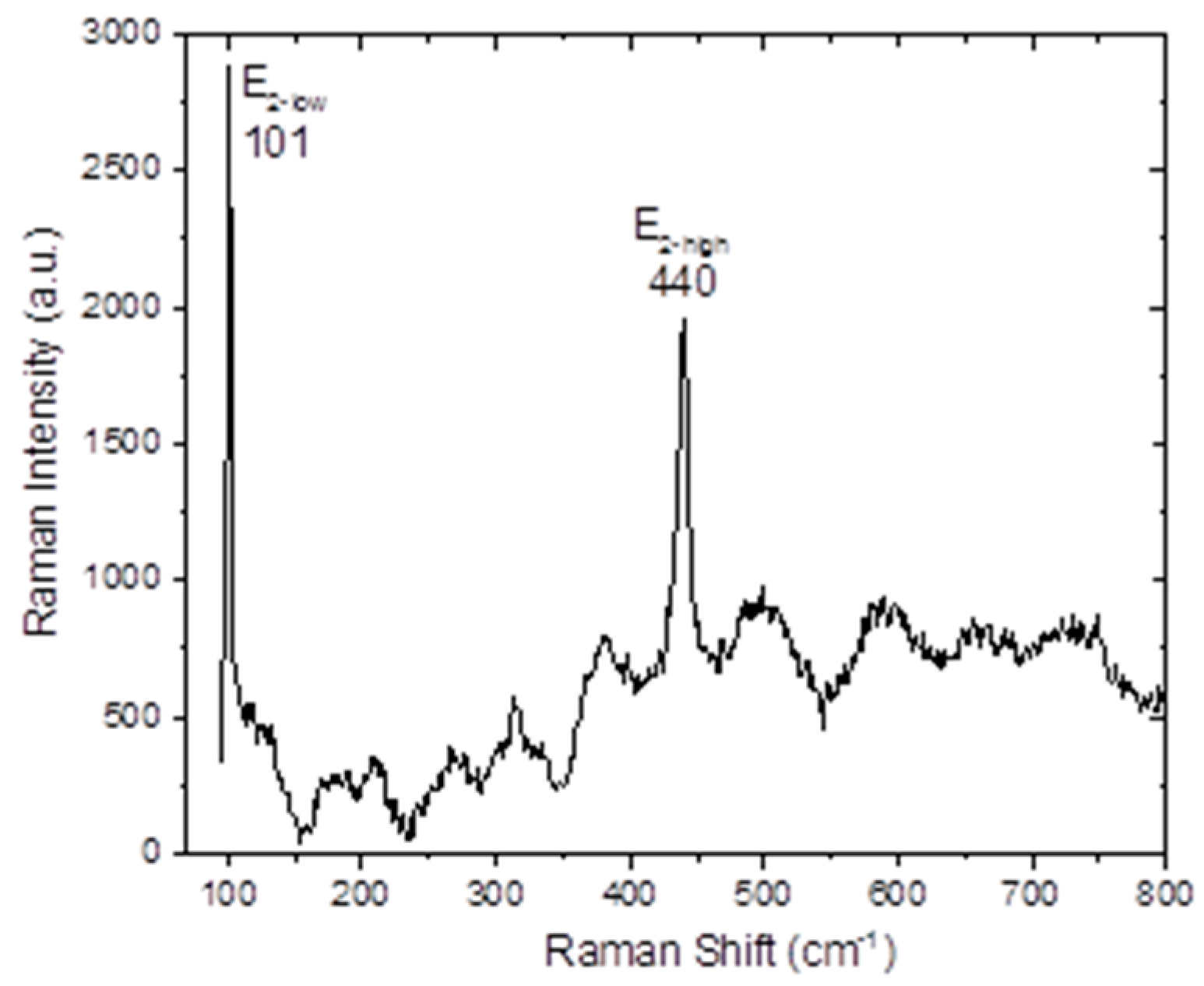
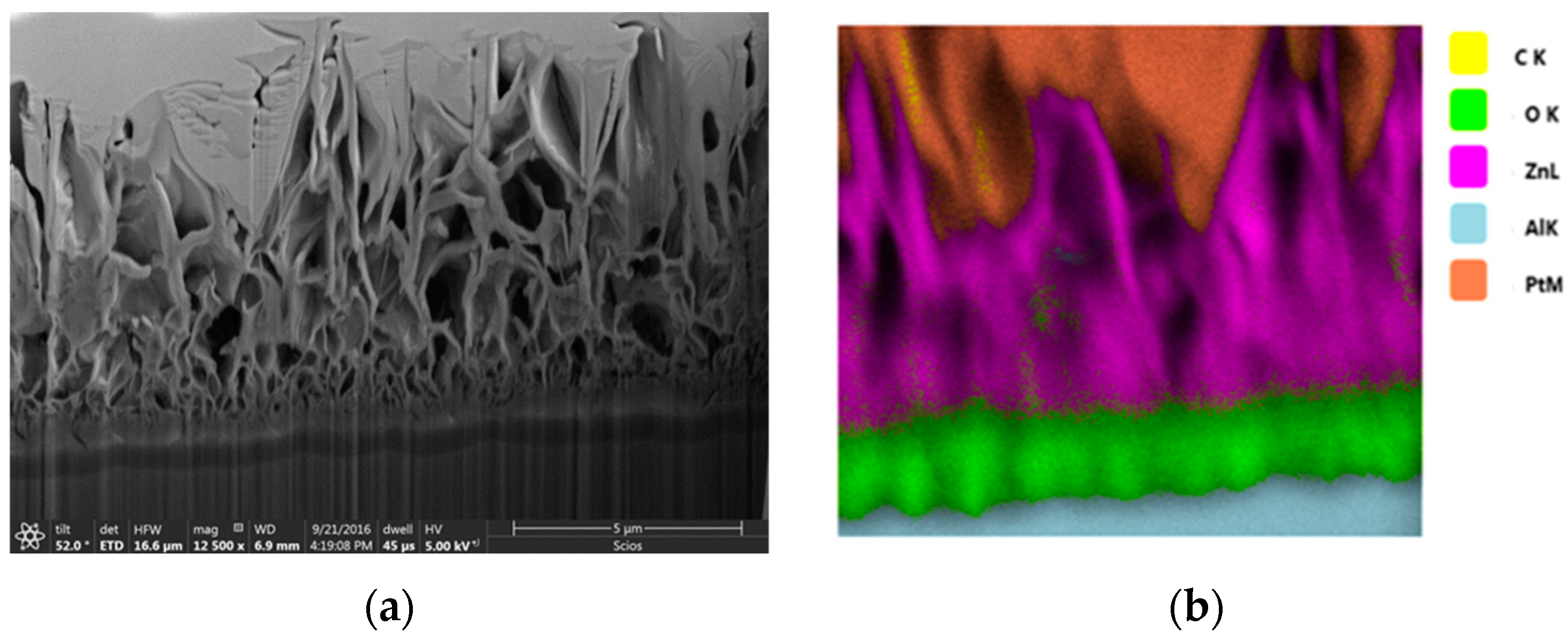
3. Results and Discussion

While the semiconductor layer was obtained through a low-temperature hydrothermal route, the substrates were prepared by subsequent electrochemical processes: electro-polishing and anodizing. The obtained MIS architecture was characterized by scanning electron microscopy (SEM), energy dispersive spectroscopy X-ray (EDS), X-ray diffraction (XRD), micro-Raman spectroscopy (µRS) and cathodoluminescence (CL). The voltage-time plot acquired during the anodizing process indicates formation of an insulating barrier (Al2O3) on the metallic substrate (Al). The SEM analysis reveals that a nanostructured layer is grown on the anodized substrate, constituted by interconnected leaf-like ZnO nanostructures with average thickness of ~50–100 nm (see Figure 3). The EDS analysis suggests formation of three different phases: ZnO, Al2O3 and Al phase (see Figure 4); the XRD results confirms the latter. According with the Raman spectrum, these ZnO nanostructures are crystalline (see Figure 3), although native defects are present as the broad visible-band centered at 533 nm in CL spectrum reveals (see Figure 4). Nowadays, the electrical characteristics of a metal-oxide-semiconductor (MIS) with ZnO nanostructures are been realized, therefore it is possible to fabricate a ZnO nanostructures-based MIS architecture using chemical routes as show in Figure 5. A correlation of results structural and optical was realized.

4. Conclusions

From the results obtained in this work related to the production and characterization of ZnO nanostructures incorporated on anodized aluminum substrates, the following conclusions were obtained. It is possible to construct a MIS type structure from chemical (electrochemical and hydrothermal) routes. These methods are characterized by using mild reaction conditions, being fast, low cost and easy processing, making possible their scaling. The study of the electropolished surface of the metal substrate (Al) by metallographic analysis shows a uniform surface, with no apparent roughness. The analysis by SEM confirmed the observed by metallography obtaining a high homogeneity of the surface of electropolished aluminum substrates.

Author Contributions

R. J. Aranda García1, A. Escobedo Morales, J. A. Luna López conceived and designed the experiments; R. J. Aranda García1, A. Escobedo Morales, J. Carrillo López, M. Dominguez, N. Carlos Ramírez performed the experiments; R. J. Aranda García, A. Escobedo Morales, J. A. Luna López analyzed the data; R. J. Aranda García, A. Escobedo Morales, M. Dominguez, N. Carlos Ramírez and J. A. Luna López wrote the paper.

Acknowledgments

This work has been partially supported by CONACyT-CB-255062 and VIEP-LULJ-EXC-2017. The authors acknowledge CIDS, INAOE and IFUAP laboratories for their help in the samples characterizations.

Conflicts of Interest

The authors declare no conflict of interest.

References

  1. Li, W.; Reisdorffer, F.; Nguyen, T.P.; Kwok, H.L. Electronic properties of ZnO nanorod MIS structure. Sci. Mater. Electron. 2013, 24, 3788–3792. [Google Scholar] [CrossRef]
  2. Diggle, J.W.; Downie, T.C.; Goulding, C.W. Porous Anodic Aluminum Oxide: Anodization and Templated Synthesis of Functional Nanostructures. Chem. Rev. 1969, 69, 365–405. [Google Scholar] [CrossRef]
  3. Amin, G.; Willander, P.M. ZnO and CuO Nanostructures: Low Temperature Growth, Characterization, Their Optoelectronic and Sensing Application; Linköping University Electronic Press: Linköping, Sweden, 2012; pp. 238–256. [Google Scholar]
Figure 1. Experimental assembly used for electropolishing and anodizing processes.
Proceedings 01 00308 g001
Figure 2. (a) Teflon device used for the growth of ZnO nanostructures on an anodized aluminum substrate; (b) experimental setup used for the growth of ZnO nanostructures.
Proceedings 01 00308 g002
Figure 3. SEM micrographs of ZnO nanostructures hydrothermally grown on the anodized aluminum substrate.
Proceedings 01 00308 g003
Figure 4. Raman spectrum of the ZnO nanostructures grown on the anodized aluminum substrate.
Proceedings 01 00308 g004
Figure 5. (a) SEM micrograph showing the cross-sectional cut made by FIB of the MIS-type structure; (b) Elemental mapping performed in each of the layers that form the MIS-type structure.
Proceedings 01 00308 g005
Publisher’s Note: MDPI stays neutral with regard to jurisdictional claims in published maps and institutional affiliations.

