Silicon Sacrificial Layer Technology for the Production of 3D MEMS (EPyC Process) †

1
Robert Bosch GmbH, Reutlingen D-72762, Germany
2
Department of Electrical Engineering and Information Technology and Fraunhofer Institute for Electronic Nano Systems ENAS Chemnitz, Technical University Chemnitz-Zwickau, Chemnitz D-09107, Germany
*
Author to whom correspondence should be addressed.
†
Presented at the Eurosensors 2017 Conference, Paris, France, 3–6 September 2017.
Proceedings 2017, 1(4), 295; https://doi.org/10.3390/proceedings1040295
Published: 11 August 2017
(This article belongs to the Proceedings of Proceedings of Eurosensors 2017, Paris, France, 3–6 September 2017)
Abstract
:The EPyC process uses silicon sacrificial layer technology, which makes it possible to generate high volume sacrificial structures of up to 100 microns thickness. The biggest challenge is the rapid and complete removal of the 3D sacrificial structure at the end of the process. This paper examines and compares in detail two silicon dry etching methods to optimize a new silicon etching process for successful EPyC manufacturing.
1. Introduction
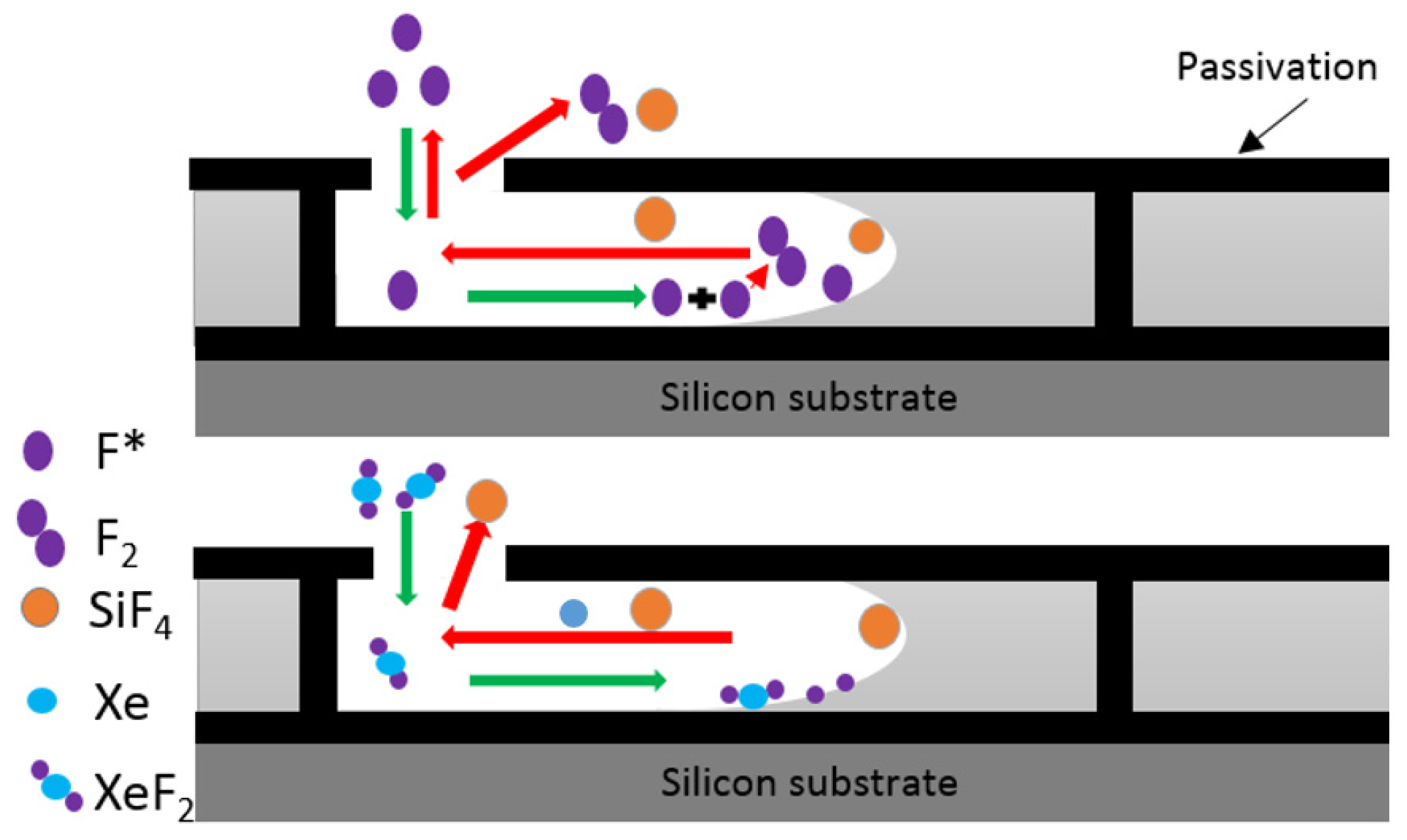
The EPyC process is based on cyclic deposition of epitaxial polysilicon and oxide. The silicon is structured by DRIE process to separate sacrificial from functional silicon. The narrow trench gaps are refilled with oxide to protect the functional parts towards the etch gases. The sacrificial structure is finally released by a suitable silicon dry etching process. The remaining oxide passivation is cleaned off the surfaces with HF vapor phase etching. An optimized dry etching process is crucial for the EPyC process [1]. The challenge is to completely remove three dimensional high volume polysilicon sacrificial structures with a high etching rate even in nested areas which are difficult to access. In this paper, two dry etching processes are examined in detail and compared with each other with regard to the requirements of the EPyC process: the plasma process with sulfur hexafluoride (SF6) and the chemical etching process with xenon difluoride (XeF2). Both etching methods etch silicon spontaneously and isotropically.
2. Silicon Dry Etching
2.1. Chemical Etching Process with XeF2
At room temperature the solid XeF2 has a vapor pressure of about 4 Torr. The gaseous XeF2 spontaneously etches silicon. The chemical reaction is shown in Equation (1).
with this etching process, it is possible to create long undercuts even within extremely narrow structures (<1 μm). However, the etch rate is limited by the vapor pressure of the solid XeF2. The etching mechanism has already been described in detail in various papers [2,3,4].
2.2. The Plasma Process with SF6
In the plasma high-energy electrons collide with -molecules and decompose into -ions and F-radicals (Equation (2)). The F-radicals react spontaneously with silicon and form the volatile product silicon tetrafluoride (Equation (3)).
The F-radicals also etch silicon isotropically. The limitation of this process is the recombination of the F-radicals [5].
In Figure 1 the etch mechanisms of SF6 and XeF2 is shown.
3. Sample Preparation
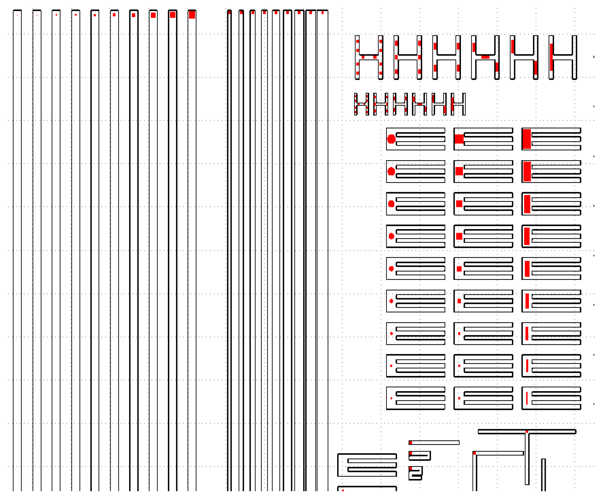
To elucidate the differences between two etching methods, a new set of masks was developed to build up a single EPyC sample for the baseline experiments. For the experiments one-sided polished 8-inch silicon substrate was used. First a 2.5 μm thermal oxide is deposited on the substrate (isolation layer). On a thin LPCVD polysilicon seed layer a 20 μm epitaxial silicon layer is grown and planarised by CMP (chemical mechanical polishing). The first mask is used to pattern the 20 μm silicon layer by DRIE process. A selection of different shapes for the sacrificial silicon is defined by the 1.4 μm single gap size mask (black line in Figure 1). The narrow trench gaps are then refilled with 2.2 μm LPCVD oxide. The second mask is used to pattern the oxide layer to create a variety of differently shaped etch accesses for SF6 and XeF2 (red areas in Figure 2). The oxide is structured by a CF4 plasma process. The final open area (etch access) with respect to the wafer surface is 0.37%. In our experiments the single EPyC samples are etched stepwise (time intervals) either with XeF2 or SF6 -plasma. Both etching processes with XeF2 and SF6 were tuned to get the maximum etch rate. The low open area of 0.37% allows high etch rates even for the vapor pressure limited XeF2. To determine the lateral etch rate the undercut is measured through the oxide mask by optical microscope.
4. Results
4.1. Aperture Size Effect
To determine the lateral undercut as a function of the size of the aperture 5000 μm long and 40 μm wide channels with a square shaped etch access on one end were used. The aperture varies from 2 × 2 to 30 × 30 μm2 in. Figure 3 show the lateral undercut as a function of the aperture size for SF6 and XeF2 after 8 min etch time respectively. For SF6 silicon is hardly etched with small aperture sizes. Between 7 × 7 μm2 and 15 × 15 μm2 the lateral undercut strongly increases. At 15 × 15 μm2 the lateral undercut starts to saturate and remains nearly constant with a maximum etch rate of ~30 μm/ min. The smaller the access the less fluorine radicals can pass the bottle neck per time unit. In addition the collision probability increases with decreasing access size leading to a strong loss of reactive fluorine radicals due to recombination. Therefore the etch slows down dramatically. With XeF2 etches silicon already with an aperture size of 2 × 2 μm2 with 3 μm/min. The etch rate strongly increases between 2 × 2 μm2 and 15 × 15 μm2 where saturation sets in with a maximum etch rate of ~37 μm/min. XeF2 shows the same limitation due to diffusion through small cross section access holes but there is no further loss of active species due to chemical reactions.
4.2. Channel Size Effect
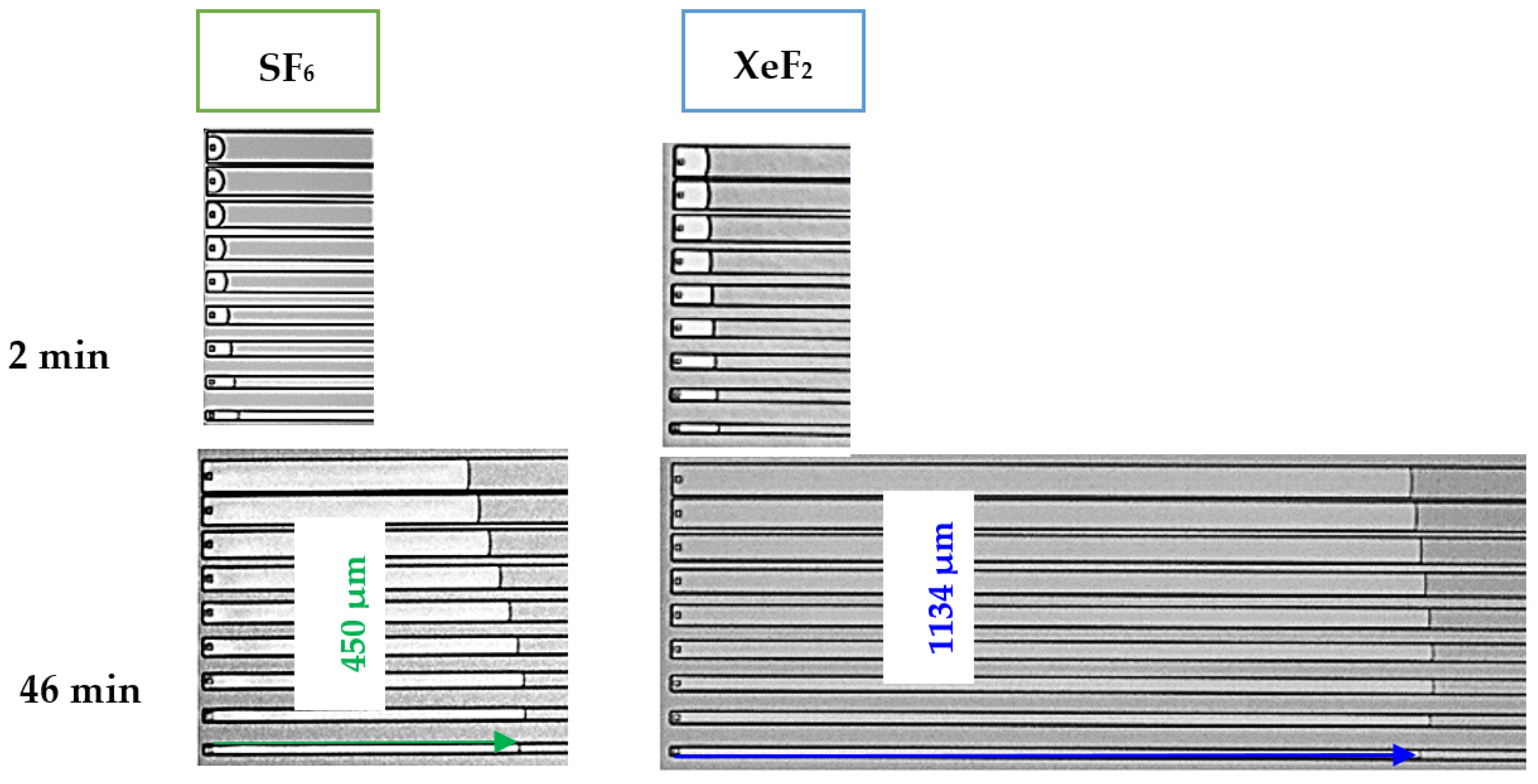
The influence of the channel width on the lateral undercut was investigated by using 5000 μm long channels with a fixed square shaped access of 10 × 10 μm2 (fixed etch gases quantity) on one end. The channel width was varied between 15.6 and 55.6 μm in 5 μm steps. By varying the width of the channels the volume of sacrificial silicon to be removed changes. The Figure 4 shows the etch results after 2 min and 46 min for SF6 and XeF2. At the beginning etching in all channels is isotropic. After 2 min of etching with XeF2 the narrow channel (15.6 μm) shows the longest undercut as expected. As the etch is continued the same etch rate is observed in all different channels. The reaction speed by XeF2 is limited by diffusion only. SF6 shows a larger difference between the channels after 2 min of etching. Therefore there might be no excess of F-radicals during the isotropic part of the etch leading to an additional advantage for the narrow channel. Continuing the etch all channels show very similar etch rates. After 46 min SF6 shows significantly shorter undercut (450 μm) then XeF2 (1134 μm). SF6 is limited by recombination in a small accesses and diffusion.
4.3. Optimization of the Etching Process by Combining SF6 and XeF2
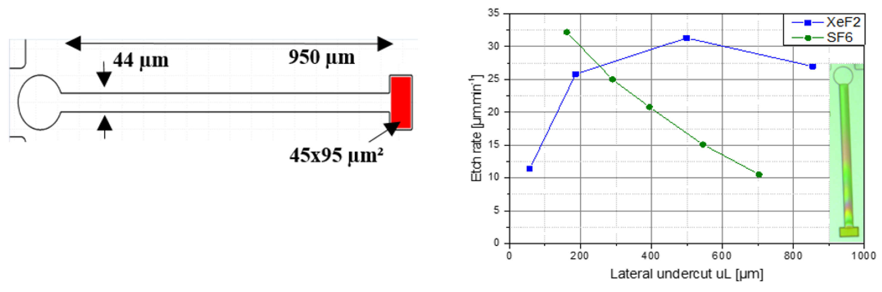
To demonstrate the advantage of a process combining SF6 and XeF2 we used a sample with larger open area of ~1%. XeF2 has a clear disadvantage etching high volumes with large open area (vapor pressure). A structure was examined with a larger rectangular access of 45 μm width and 95 μm length. The channel to be etched is 950 μm long and 44 μm wide. In Figure 5 it is shown that the etch rate of SF6 at the beginning etching is by a factor 3 higher than the etch rate of XeF2. Then decreases the etch rate of SF6 with the undercut contrary to XeF2 where the etch rate increases with the undercut since the open area of silicon decreases during the etch process. There is a certain undercut length of ~200 μm where XeF2 begins to etch faster than SF6. The etch time can be reduced by a factor of 2 to 28 min by combining both etch methods. The optimum undercut to switch etch gases strongly depends on the layout (open area, aperture size, layer thickness).
5. Conclusions
In this paper two dry etching processes were investigated in detail with regard to the requirements of the EPyC process. The plasma-process with sulfur hexafluoride (SF6) shows its strength in etching high volumes. Vertical etching in the depth and lateral undercut of readily accessible sacrificial silicon of up to 300 μm is possible with very high etch rate of 30–40 μm/min. The etching rate decreases with increasing undercut. Furthermore, the etch-rate almost comes to a standstill with small etching accesses d < 6 μm. The chemical etching process with xenon difluoride (XeF2) gas behaves completely different. The strength is in the etching of small volumes in nested sacrificial structures with extreme undercut of > 300 μm. In this case, etching rates of 30–40 μm/min can also be observed in areas which are difficult to access. The etch rate drops dramatically when XeF2 faces a high open area of silicon. A big advantage was observed in combining both etching methods leading to a much shorter etching time. A rapid and complete removal of 3D sacrificial silicon structures at the end of the multi-layer EPyC process is now possible. Since the process can be adapted towards the individual requirements (high volume or tiny nested structures), the process is ready to face needs of any complexity.
Author Contributions
L.L. and P.S. conceived and designed the experiments; L.L. performed the experiments, analyzed the data, contributed reagents/materials/analysis tools; A.K. contributed in scientific discussions and interpretation of the results; L.L. and P.S wrote the paper with input from all authors. Both P.S and T.O. provided critical feedback. T.O. supervised the project.
Conflicts of Interest
The authors declare no conflict of interest.
References
- Breitschaedel, O.; Kaelberer, A.; Zielke, C.; Staffeld, P.B.; Artmann, H. Method for Manufacturing Microelectromechanical Structures in A Layer Sequence and a Corresponding Electronic Component Having a Microelectromechanical Structure. US Patent Application 15/097,331, 20 October 2016. [Google Scholar]
- Metzger, L.; Fischer, F.; Mokwa, W. Polysilicon Sacrificial Layer Etching Using XeF2 for Silicon Acceleration Sensors with High Aspect Ratio. In Proceedings of the European Conference on Solid-State Transducers, Eurosensors XVI, Prague, Czech Republic, 15–18 September 2002. [Google Scholar]
- Chang, F.I.; Yeh, R.; Lin, G.; Chu, P.B.; Hoffman, E.; Kruglick, E.J.J.; Pister, K.S.J. Gas-phase silicon micromachining with xenon difluoride. SPIE 1995, 2641, 117–128. [Google Scholar]
- Dagata, J.A.; Squire, D.W.; Dulcey, C.S.; Hsu, D.S.Y.; Lin, M.C. Chemical processes involved in the etching of silicon by xenon difluoride. J. Vac. Sci. Technol. B 1987, 5, 1495–1500. [Google Scholar] [CrossRef]
- Anderson, H.M.; Merson, J.A.; Light, R.W. A kinetic model for plasma etching silicon in a SF6/02 RF discharge. IEEE Trans. Plasma Sci. 1986, 14, 156–164. [Google Scholar] [CrossRef]
Figure 1.
Schematic view of silicon etch process. At the beginning silicon is etched isotropic (all direction). As soon as the sacrificial silicon is cleared to the bottom oxide there is only lateral undercut restricted by the oxide filled trench gaps.
Figure 1.
Schematic view of silicon etch process. At the beginning silicon is etched isotropic (all direction). As soon as the sacrificial silicon is cleared to the bottom oxide there is only lateral undercut restricted by the oxide filled trench gaps.

Figure 2.
Mask-layers (black line: trench mask, red area: etch-access) for etch experiments. Some examples narrow/wide lines, dense/isolated.
Figure 2.
Mask-layers (black line: trench mask, red area: etch-access) for etch experiments. Some examples narrow/wide lines, dense/isolated.

Figure 3.
The etch results after 8 min for XeF2 (left) and SF6 (right).

Figure 4.
The etch results after 2 min and 46 min for XeF2 and SF6.

Figure 5.
Etching results for same structure of the both etching gases SF6 and XeF2 in different etching time.
Figure 5.
Etching results for same structure of the both etching gases SF6 and XeF2 in different etching time.

© 2017 by the authors. Licensee MDPI, Basel, Switzerland. This article is an open access article distributed under the terms and conditions of the Creative Commons Attribution (CC BY) license (https://creativecommons.org/licenses/by/4.0/).
Share and Cite
MDPI and ACS Style
Louriki, L.; Staffeld, P.; Kaelberer, A.; Otto, T. Silicon Sacrificial Layer Technology for the Production of 3D MEMS (EPyC Process). Proceedings 2017, 1, 295. https://doi.org/10.3390/proceedings1040295
AMA Style
Louriki L, Staffeld P, Kaelberer A, Otto T. Silicon Sacrificial Layer Technology for the Production of 3D MEMS (EPyC Process). Proceedings. 2017; 1(4):295. https://doi.org/10.3390/proceedings1040295
Chicago/Turabian StyleLouriki, Latifa, Peter Staffeld, Arnd Kaelberer, and Thomas Otto. 2017. "Silicon Sacrificial Layer Technology for the Production of 3D MEMS (EPyC Process)" Proceedings 1, no. 4: 295. https://doi.org/10.3390/proceedings1040295