Article

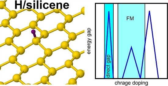
Tuning the Electronic Structure of Hydrogen-Decorated Silicene

by
Agata Podsiadły-Paszkowska
* and
Mariusz Krawiec
Institute of Physics, Maria Curie-Skłodowska University, Pl. M. Curie-Skłodowskiej 1, 20-031 Lublin, Poland
*
Author to whom correspondence should be addressed.
Condens. Matter 2017, 2(1), 1; https://doi.org/10.3390/condmat2010001
Submission received: 9 November 2016 / Revised: 15 December 2016 / Accepted: 19 December 2016 / Published: 23 December 2016

Abstract

:
The effects of strain, charge doping, and external electric field on the electronic structure of a free-standing silicene layer decorated by hydrogen atoms are studied by first-principles density functional theory. Various phases, including insulating, metallic, spin-polarized, and half-metallic have been found, depending on these external factors. The most efficient way of switching the system between these phases is charge doping. The character of the energy gap of the H/silicene system can also be modified, and for charged or for strained systems, the originally indirect gap can be tuned to become direct. The obtained results are very promising in view of the silicene functionalization and potential applications of silicene in the fields of spintronics and optoelectronics.

Graphical Abstract

1. Introduction

Two-dimensional materials have been an area of intense research focus in recent years due to their unusual transport properties [1,2,3]. One of the particularly intensively studied materials is silicene (silicon equivalent of graphene), showing the same atomic structure as a monolayer of atoms arranged in a honeycomb lattice [4,5,6,7]. This material is also twin of graphene in terms of energy structure, with bands of linear dispersion derived from the π-type bonds [8,9,10]. In spite of numerous similarities between silicene and graphene, many differences make silicene more attractive from the point of view of possible applications in the current and future electronics. Silicene enables a significant improvement in the current devices based mainly on silicon, minimizing them with much less effort than would be required in the conversion from silicon technology to technology based on graphene.
Unfortunately, the essential drawback of silicene is the difficulty in preparing it such that its two-dimensional character—and thus excellent transport properties—are not damaged. An intense discussion on silicene on silver (the most commonly used as a substrate for silicene growth) showed that silicon atoms bind too strongly to silver, so that they do not form a two-dimensional quasi-freestanding crystal [11,12,13,14,15,16,17,18,19,20,21]. Several other surfaces have been used to produce silicene [22,23,24], and others have been proposed as potentially suitable for silicene formation [25,26,27,28,29,30,31,32], but the problem still does not have a clear solution. Another problem is the exposure of silicene to ambient conditions [33]. However, Tao et al. reported the first field-effect transistor based on silicene on a thin Al 2 O 3 layer obtained using the novel method of encapsulated delamination from silicene on Ag(111) [34].
Despite these disadvantages, intensive theoretical work is aimed at predicting the features of silicene under different conditions. Unlike graphene, freestanding silicene exhibits a corrugated structure on the atomic scale, which is associated with the mixed sp 2 and sp 3 hybridization of their atomic orbitals [8,9,35]. Such a structure makes silicene much more susceptible to functionalization.
The studies indicate that with only adsorption of foreign element atoms on silicene, its transport and magnetic properties can be modulated in a wide range such that silicene behaves like a semiconductor, metal, insulator, or a half-metal with magnetic ordering [36,37,38,39,40,41]. However, other methods of affecting the atomic and electronic structure of silicene are also commonly used; e.g., electric field, charge doping, and strain [42,43,44,45,46,47].
Recently, studies that combine several methods for the functionalization of silicene are also under consideration—for example, a combination of the electric field and strain shows the possibility of increasing the band gap caused by the spin–orbit interaction [48]. Moreover, both tensile strain and electric field were proved to enhance adsorption of hydrogen on silicene [49,50]. Silicane—a fully hydrogenated silicene layer—is also under consideration thanks to its mechanical and transport properties [51,52,53,54]. Although it is not possible to produce silicane experimentally, the studies on the hydrogenation of silicene on Ag(111) (e.g., half-hydrogenated silicene) have shown that it can be employed as a method of modifying silicene properties, and indicated that the structure 2 3 × 2 3 R 30 contains no defects or alloy with Ag [55], contrary to the earlier reports [56,57]. It has also been shown that the hydrogenation of silicene is a reversible process and can be effectively used for hydrogen storage [58]. Still, future applications of silicene demand a profound analysis of possible external factors that will influence its properties and possibly increase its utility.
In our previous paper [59], we investigated structural, kinetic, and magnetic properties of hydrogen-decorated free-standing silicene subjected to external electric field, charge doping, uniform and nonuniform strains. It was shown that the charge doping and the strain are the most effective ways of changing the hydrogen–silicene binding energy. The strain also has the strongest impact on the diffusion of H atoms, and can change the diffusion barrier by 50%. The system in its equilibrium is a ferromagnet with locally antiferromagnetic order, and can easily be driven into a nonmagnetic phase by the charge doping and strain.
The purpose of this paper is to show how to modify and control the electronic properties of the system (such as magnitude and character of a band gap) by charge doping, external electric field, and uniform and nonuniform strains. We show that these methods allow significant modifications of the band gap and the magnetic ordering of the system. The most effective way of tuning the electronic properties is charge doping. It can drive the originally spin-polarized insulating H/silicene system to various phases, including non-magnetic insulating, metallic (magnetic or non-magnetic), and half-metallic. The character of the band gap can also be modified and switched from an indirect to a direct one in a charged or strained H/silicene system. These findings are very promising in view of silicene functionalization and potential applications of silicene in the fields of spintronics and modern optoelectronics.

2. Details of Calculations

The calculations were performed within density functional theory (DFT) using the Siesta code [60,61,62,63,64]. The exchange-correlation energy was used in Perdew–Burke–Ernzerhof form [65] of the generalized gradient approximation (GGA), and Troullier–Martins norm-conserving pseudopotentials [66] were used to simulate the core–electrons interaction. The Brillouin zone (BZ) was sampled by 30 × 30 × 1 k-points, and the energy cutoff was set to 300 Ry in all the calculations.
The system was modeled as the 4 × 4 unit cell of silicene with a single H atom above one of the Si atoms. Such a unit cell allows interaction between neighboring hydrogen atoms to be avoided, and corresponds to the uniform coverage of one H atom per 32 Si atoms (i.e., θ = 1 / 32 ). The system was relaxed to the maximum forces below 0.01 eV/Å. The lattice constant for the system in equilibrium conditions was equal to 3.87 Å, which is very close to the value for a freestanding layer; thus, the presence of a hydrogen atom does not strongly affect the atomic structure of silicene. However, the methods in use do affect this value, and the lattice constant was modified and adjusted for any considered case.
The uniform strain ε is defined as ( a a 0 ) / a 0 , where a and a 0 are the lattice constants of the strained system and the system in its equilibrium, respectively. The uniform strain was modeled by changing a. In the calculations for a nonuniformly strained system, the lattice constant was changed in the zigzag (ZZ) direction ( ε ZZ ), while the system was allowed to relax in the armchair (AC) direction, and thus the effect of strain was partially compensated. Using this method, we analyzed the lattice deformation in both perpendicular directions simultaneously, as tensile strain in one direction is accompanied by compression in the other direction, and vice versa.

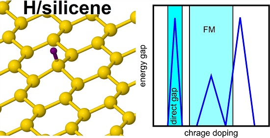
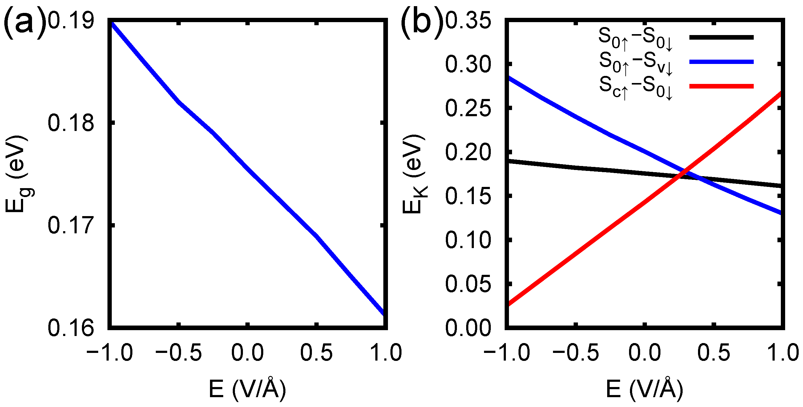
3. Results and Discussion

In equilibrium (i.e., without any external perturbations), the H/silicene system is a ferromagnetic insulator, although with locally antiferromagnetic order [40,59]. The insulating character is a direct consequence of the inversion symmetry breaking due to the adsorption of an H atom [19,26,67,68]. The adsorbed H atoms are also responsible for the magnetism of the system, as they break the silicene π bonds, and two dangling p z orbitals are formed. One orbital is involved in the bonding with the H atom, while the other one forms the spin-polarized state localized in the vicinity of the adsorbed H atom [59].
A fully-hydrogenated silicene may be an indirect- or a direct-gap semiconductor, depending on the atomic configuration [69]. At lower H coverage (like discussed here), the system is an indirect band gap insulator [40], which somehow limits its potential applications in nanoelectronics. The adsorption of H atoms leads to a large energy gap between the valence S v and conduction S c bands at the K point of the silicene Brillouin zone, and to in-gap flat bands S 0 , as demonstrated in Figure 1b.
The flat bands substantially suppress the energy gap, which in the present case yields 100 meV, a value slightly larger than in the previous studies [40]. These bands are spin polarized, and were previously misinterpreted as the bands mainly derived from H orbitals [40]. If it was true, the H atoms should feature large magnetic moments (μ), which is not the case, as μ = 0.05 μ B [59]. Thus, the origin of the S 0 bands must be different. Indeed, these bands come mainly from dangling p z orbitals of Si atoms—nearest neighbors of the H adsorption site, marked as Si 1 in Figure 1a. Each of these atoms carries higher magnetic moment (0.20 μ B ) than the H atom. This scenario is fully confirmed by the projected band structure, shown in Figure 1c,d. Clearly, the main contribution to the spin-polarized flat bands around the Fermi energy E F comes form the 3 p z orbitals of Si 1 atoms, not from the H adatom. Similar conclusions have also been drawn in a very recent study [70]. Moreover, the Si 3 atoms also contribute to these states (see Figure S1 of Supplementary Materials), as they carry more than half of the magnetic moment of Si 1 atoms [59]. The contribution of the remaining atoms is much smaller or even negligible.
The above shows that the H/silicene system in equilibrium is an indirect-gap ferromagnetic insulator. This situation may change if the external factors (such as charge doping, strain or electric field) come into play. As a result, the value and character of the energy gap, as well as the magnetic properties of the system can be tuned and controlled.
Placing freestanding silicene in an electric field perpendicular to its plane induces polarization of its sublattices, which leads to the opening of an energy gap. It was shown that the width of this energy gap grows linearly in a wide range of electric field intensity [43]. In the present case, the symmetry between sublattices is already broken due to the adsorption of H atoms, and the charge distribution is inhomogeneous. Since the hydrogen atom attracts negative charge, the top silicene sublattice is charged positively, and the bottom one negatively, even without an external electric field [59]. Thus, unlike freestanding silicene, the insulating character of the H/silicene structure is observed at equilibrium. When the negative (positive) perpendicular electric field is applied to the H/silicene plane, the polarization between sublattices is enhanced (suppressed), which results in the widening (narrowing) of the energy gap. The situation is illustrated in Figure 2.
Note that electric field does not change the character of the energy gap. Only its magnitude changes linearly with the field. It does not spoil the magnetic order either [59]. The main effect of the electric field is the shifting of the whole band structure—except S 0 states, which are pinned at the E F (see Figure S2). This is reflected in separations between S 0 and S c ( v ) bands, shown in Figure 2b. Going from negative to positive values of the electric field, the S c and S v bands move up towards higher energies. At much higher—perhaps unrealistic—positive (negative) electric field (not shown), the S 0 and S v (S c ) of the same spin channel overlap and start to hybridize, which leads to a transition into a non-magnetic metallic phase. However, in this case, the structure may not be stable. Thus, the electric field maintains the equilibrium properties of the H/silicene system, and only tunes the magnitude of the energy gap.
When silicene is formed on the surface, the charge transfer always occurs [71,72]; thus, we analyze the influence of charge doping on the system. It is well known that the effect of additional charge introduced to a system results in an almost rigid shift of electron bands [73]. Indeed, such a shift of the bands with no band-gap opening has been predicted for freestanding silicene, since the additional charge is distributed equally on both sublattices [42]. As mentioned previously, when an H atom adsorbs on a silicene layer, sublattice polarization is induced and the energy gap develops. Thus, besides the trivial shift of the electron bands, we can also expect other modifications of the electronic structure.
The additional negative charge is transferred to the hydrogen atom, but it partially remains in the layer and reduces the sublattices’ polarization. However, if the electrons are subtracted from the system, but the hydrogen atom is still negatively charged, the sublattices’ polarization increases [59]. Thus, in the former case, the energy gap should narrow, while in the latter case, it should widen. However, the situation is more complicated, as shown in Figure 3a.
First of all, we should remember that the ground state of the H/silicene system is magnetic with a non-zero energy gap. Furthermore, the magnetism is governed by the quasi-localized S 0 states, and disappears for both electron and hole doping higher than 0.05 per primitive ( 1 × 1 ) cell [59]. Above these values of doping, the S 0 states are below or above the E F (see Figure S3), which means that the dangling 3 p z orbitals of Si atoms are fully occupied or empty, and thus no net spin is present. Obviously, the electronic spectrum is gapped. However, the energy gap for the undoped system develops between spin-polarized S 0 states, while at higher doping (i.e., in the nonmagnetic state), the energy gap appears either between S c and S 0 or between S 0 and S v states, depending on the nature of the doping. For the electron doping, the originally indirect band gap changes into a direct one, as the Fermi level falls in between S c and S 0 states (see Figure S3). For the hole doping, the band gap still is indirect. Thus, to think about applications in optoelectronics, one should dope the H/silicene system by electrons. Further increase of doping results in ordinary metallic character of the bands associated with crossing the E F either by S c or by S v .
The transition from the magnetic to nonmagnetic gapped phase is accompanied by the gap closing at low charge doping, but still maintaining the non-zero spin polarization. Interestingly, one can tune the band structure in such a way that electrons with only one spin orientation will be mobile; i.e., the system becomes a half-metal with 100% spin polarization (see Figure S3b,e). A similar phase has also been predicted in the case of the adsorption of single Ti and Cr atoms and for half-brominated silicene [36,37]. However, it is important to realize that the metallic character associated with the S 0 states should be taken with care, as these states are very weakly dispersive, and thus quasi-localized—it might be difficult to utilize them in spintronics applications. Perhaps the solution to this problem might be increasing the H coverage, which makes these states more dispersive [40,70].
Thus, the charge doping appears as a very efficient way of tuning the H/silicene band structure. It can drive the originally ferromagnetic insulator through the ferromagnetic metal, half-metal to an ordinary nonmagnetic insulator, and then to an ordinary metal. It can also change the character of the band from indirect to direct.
The strongest impact on the energetics of the H/silicene system was due to tension and compression of the silicene layer, as it leads to the most dramatic changes in the nature of bonds [59]. Thus, we also expect substantial modifications in the electronic properties of H-decorated silicene. Figure 3b shows the variation of the energy gap as a function of the uniform strain ε.
The band structure is gapped only for tensile strain up to ε = 0.10 . In this region (i.e., 0 ε < 0.10 ), the ground state does not alter its equilibrium phase (i.e., the system is a ferromagnetic insulator). Unlike the case of the charge-doped H/silicene, the band gap in the strained system always occurs between spin-polarized S 0 states, as Figure S4 shows. Interestingly, for small positive values of ε (marked in Figure 3b), the character of the gap changes from indirect to direct, which points to the possibility of utilizing strained H/silicene in applications.
When either uniform compression or uniform stretching with ε > 0.10 is applied to the silicene layer, the system becomes metallic. However, these insulator–metal transitions have different origins. The gap closing for ε < 0 is accompanied by the suppression of magnetism, while for ε > 0.10 , the system is still in the ferromagnetic phase (see Figure S4a,f). The metallic phase at the compressive strain is achieved owing to the structural phase transition. The originally low buckled silicene enters the rippled phase as soon as the compression is applied to the system [59]. On the other hand, at large tensile strain, the insulator–metal transition is associated with the flattening of the silicene layer and charge transfer from π to σ bands (see the modifications of the band structure near the Γ point, shown in Figure S4e,f). The system is stable in a wide range of tensile strain. It does not disintegrate even for ε = 0.17 , which is known to be the limit of silicene and silicane mechanical stability [74,75].
The nonuniform strain ε ZZ applied to the H/silicene layer in the zigzag direction leads to essentially very similar results to the case of the uniform strain, although a few differences do exist. First of all, K 1 and K 2 points in the Brillouin zone are no longer equivalent, since the uniform strain changed the shape of BZ, as Figure 3c shows.
Thus, the band structures in Γ K 1 and in Γ K 2 directions are different, which results in different magnitudes of energy gaps in these directions, as Figure 3d illustrates. Note however that the Γ K 2 direction will vary with the magnitude of the ϵ ZZ as the shape of the BZ changes. Furthermore, it is known that for both free-standing graphene and silicene subjected to nonuniform tension, the Dirac cone moves from the K point of the BZ along the line connecting points Γ and K in the strain direction [76,77]. Nevertheless, the gapped phase occurs in a similar region like in the case of the uniform strain. This phase also survives in weakly compressed H/silicene system, which is associated with the fact that the lattice constant in the direction perpendicular to the strain direction is allowed to relax and keeps trying to maintain its equilibrium value [59]. The gapped phase is also magnetic, and unlike the previous case, only an indirect gap is observed. The transition to a metallic phase for negative strain is due to the same reasons as for the uniform strain. For large values (over 0.075) of both positive and negative strain, the system loses its stability and disintegrates. Thus, the uniform strain seems to be superior over the nonuniform strain, due to the possibility of changing the character of the energy gap.

4. Conclusions

We have analyzed the electronic and magnetic properties of H-decorated silicene subjected to external factors such as charge doping, electric field, and uniform and nonuniform strain. We have shown that all these methods allow controlling the band gap and the magnetic ordering of the system. The most efficient method of tuning the electronic properties is charge doping. It can drive the originally spin-polarized insulating H/silicene system to various phases, including non-magnetic insulating, metallic (magnetic or non-magnetic), and half-metallic. The character of the band gap can also be modified and switched from an indirect to a direct one in charged or strained H/silicene systems. These findings reveal efficient methods of functionalization and tuning the electronic properties of silicene, and are promising from an application point of view in the fields of spintronics and modern optoelectronics.

Supplementary Materials

The following are available online at https://www.mdpi.com/2410-3896/2/1/1/s1. Figure S1: The electronic structure of H/silicene system projected on the 3 p z orbitals of different Si atoms; Figure S2: The band structure of H/silicene in external electric field; Figure S3: Variations of the band structure for doped system; Figure S4: The band structure of strained H/silicene system.

Acknowledgments

The work has been supported by the National Science Center under Grant No. DEC-2014/15/N/ST3/03816. Part of this work has been presented at the international conference on Atomically Controlled Surfaces, Interfaces and Nanostructures (ACSIN2016) held in Rome, Italy on 9–15 October 2016 [78].

Author Contributions

Agata Podsiadły-Paszkowska performed the DFT calculations; Mariusz Krawiec analyzed data; Agata Podsiadły-Paszkowska and Mariusz Krawiec wrote the paper. Both authors have read and approved the final manuscript.

Conflicts of Interest

The authors declare no conflict of interest.

References

  1. Butler, S.Z.; Hollen, M.S.M.; Cao, L.; Cui, Y.; Gupta, J.A.; Gutierrez, H.R.; Heinz, T.F.; Hong, S.S.; Huang, J.; Ismach, A.F.; et al. Progress, challenges, and opportunities in two-dimensional materials beyond graphene. ACS Nano 2013, 7, 2898–2926. [Google Scholar] [CrossRef] [PubMed]
  2. Bhimanapati, G.R.; Lin, Z.; Meunier, V.; Jung, Y.; Cha, J.; Das, S.; Xiao, D.; Son, Y.; Strano, M.S.; Cooper, V.R.; et al. Recent advances in two-dimensional materials beyond graphene. ACS Nano 2015, 9, 11509–11539. [Google Scholar] [CrossRef] [PubMed]
  3. Gupta, A.; Sakthivel, T.; Seal, S. Recent development in 2D materials beyond graphene. Prog. Mater. Sci. 2015, 73, 44–126. [Google Scholar] [CrossRef]
  4. Houssa, M.; Scalise, E.; Sankaren, K.; Pourtois, G.; Afanasev, V.V.; Stesmans, A. Electronic properties of hydrogenated silicene and germanene. Appl. Phys. Lett. 2011, 98, 223107. [Google Scholar] [CrossRef]
  5. Zhong, H.; Quhe, R.; Wang, Y.; Shi, J.; Liu, J. Silicene on Substrates: A Theoretical Perspective. Chin. Phys. B 2015, 24, 087308. [Google Scholar] [CrossRef]
  6. Le Lay, G.; Salomon, E.; Angot, T. Silicene: Silicon conquers the 2D world. Europhys. News 2016, 47, 17–21. [Google Scholar] [CrossRef]
  7. Zhao, J.; Liu, H.; Yu, Z.; Quhe, R.; Zhou, S.; Wang, Y.; Liu, C.C.; Zhong, H.; Han, N.; Lu, J.; et al. Rise of silicene: A competitive 2D material. Prog. Mater. Sci. 2016, 83, 24–151. [Google Scholar] [CrossRef]
  8. Takeda, K.; Shiraishi, K. Theoretical possibility of stage corrugation in Si and Ge analogs of graphite. Phys. Rev. B 1994, 50, 14916–14922. [Google Scholar] [CrossRef]
  9. Cahangirov, S.; Topsakal, M.; Aktürk, E.; Sahin, H.; Ciraci, S. Two- and One-Dimensional Honeycomb Structures of Silicon and Germanium. Phys. Rev. Lett. 2009, 102, 236804. [Google Scholar] [CrossRef] [PubMed]
  10. Sahin, H.; Cahangirov, S.; Topsakal, M.; Bekaroglu, E.; Aktürk, E.; Senger, R.T.; Ciraci, S. Monolayer honeycomb structures of group-IV elements and III-V binary compounds: First-principles calculations. Phys. Rev. B 2009, 80, 155453. [Google Scholar] [CrossRef]
  11. Vogt, P.; De Padova, P.; Quaresima, C.; Avila, J.; Frantzeskakis, E.; Asensio, M.C.; Resta, A.; Ealet, B.; Le Lay, G. Silicene: Compelling Experimental Evidence for Graphenelike Two-Dimensional Silicon. Phys. Rev. Lett. 2012, 108, 155501. [Google Scholar] [CrossRef] [PubMed]
  12. Fleurence, A.; Friedlein, R.; Ozaki, T.; Kawai, H.; Wang, Y.; Yamada-Takamura, Y. Experimental Evidence for Epitaxial Silicene on Diboride Thin Films. Phys. Rev. Lett. 2012, 108, 245501. [Google Scholar] [CrossRef] [PubMed]
  13. Jamgotchian, H.; Colington, Y.; Hamazaouri, N.; Ealet, B.; Hoarau, J.; Aufray, B.; Biberian, J.P. Growth of silicene layers on Ag(111): Unexpected effect of the substrate temperature. J. Phys. Condens. Matter 2012, 24, 172001. [Google Scholar] [CrossRef] [PubMed]
  14. Chiappe, D.; Granzietti, C.; Tallarida, G.; Fanciulli, M.; Molle, A. Local Electronic Properties of Corrugated Silicene Phases. Adv. Matter 2012, 24, 5088–5093. [Google Scholar] [CrossRef] [PubMed]
  15. Majzik, Z.; Tchalala, M.R.; Svec, M.; Hapala, P.; Enriquez, H.; Kara, A.; Mayne, A.J.; Dujardin, G.; Jelinek, P.; Oughaddou, H. Combined AFM and STM measurements of a silicene sheet grown on the Ag(111) surface. J. Phys. Condens. Matter 2013, 25, 225301. [Google Scholar] [CrossRef] [PubMed]
  16. Chen, L.; Liu, C.C.; Feng, B.; He, X.; Cheng, P.; Ding, Z.; Meng, S.; Zao, Z.G.; Wu, K.H. Evidence for Dirac Fermions in a Honeycomb Lattice Based on Silicon. Phys. Rev. Lett. 2012, 109, 056804. [Google Scholar] [CrossRef] [PubMed]
  17. Wang, Y.; Cheng, H. Absence of a Dirac cone in silicene on Ag(111): First-principles density functional calculations with a modified effective band structure technique. Phys. Rev. B 2013, 87, 245430. [Google Scholar] [CrossRef]
  18. Guo, Z.; Furuya, S.; Iwata, J.I.; Oshiyama, A. Absence and presence of Dirac electrons in silicene on substrates. Phys. Rev. B 2013, 87, 235435. [Google Scholar] [CrossRef]
  19. Lin, C.; Arafune, R.; Kawahara, K.; Kanno, M.; Tsukahara, N.; Minamitani, E.; Kim, Y.; Kawai, M.; Takagi, N. Substrate-Induced Symmetry Breaking in Silicene. Phys. Rev. Lett. 2013, 110, 076801. [Google Scholar] [CrossRef] [PubMed]
  20. Feng, B.; Li, H.; Liu, C.; Shao, T.; Cheng, P.; Yao, Y.; Meng, S.; Chen, L.; Wu, K. Observation of Dirac Cone Warping and Chirality Effects in Silicene. ACS Nano 2013, 10, 9049–9054. [Google Scholar] [CrossRef] [PubMed]
  21. Feng, Y.; Liu, D.; Feng, B.; Liu, X.; Zhao, L.; Xie, Z.; Liu, Y.; Liang, A.; Hu, C.; Hu, Y.; et al. Direct Evidence of Interaction-Induced Dirac Cones in Monolayer Silicene/Ag(111) System. 2015; arXiv:1503.06278. [Google Scholar]
  22. Meng, L.; Wang, Y.; Zhang, L.; Du, S.; Wu, R.; Li, L.; Zhang, Y.; Li, G.; Zhou, H.; Hofer, W.A.; et al. Buckled Silicene Formation on Ir(111). Nano Lett. 2013, 13, 685–690. [Google Scholar] [CrossRef] [PubMed]
  23. Morishita, T.; Spencer, M.J.S.; Kawamoto, S.; Snook, I.K. A New Surface and Structure for Silicene: Polygonal Silicene Formation on the Al(111) Surface. J. Phys. Chem. C 2013, 117, 22142–22148. [Google Scholar] [CrossRef]
  24. Aizawa, T.; Suehara, S.; Otani, S. Silicene on Zirconium Carbide (111). J. Phys. Chem. C 2014, 118, 23049–23057. [Google Scholar] [CrossRef]
  25. Cai, Y.; Chuu, C.P.; Wei, C.; Chou, M.Y. Stability and electronic properties of two-dimensional silicene and germanene on graphene. Phys. Rev. B 2013, 88, 245408. [Google Scholar] [CrossRef]
  26. Liu, H.; Gao, J.; Zhao, J. Silicene on Substrates: A Way To Preserve or Tune Its Electronic Properties. J. Phys. Chem. C 2013, 117, 10353–10359. [Google Scholar] [CrossRef]
  27. Scalise, E.; Houssa, M.; Cinquanta, E.; Grazianetti, C.; Van den Broek, B.; Pourtois, G.; Stesmans, A.; Fanciulli, M.; Molle, A. Engineering the electronic properties of silicene by tuning the composition of MoX2 and GaX (X = S, Se, Te) chalchogenide templates. 2D Mater. 2014, 1, 011010. [Google Scholar] [CrossRef]
  28. Kanno, M.; Arafune, R.; Lin, C.L.; Minamitani, E.; Kawai, M.; Takagi, N. Electronic decoupling by h-BN layer between silicene and Cu(111): A DFT-based analysis. New J. Phys. 2014, 16, 105019. [Google Scholar] [CrossRef]
  29. Zhu, J.; Schwingenschlögl, U. Structural and Electronic Properties of Silicene on MgX2 (X = Cl, Br, and I). Appl. Mater. Interfaces 2014, 6, 11675–11681. [Google Scholar] [CrossRef] [PubMed]
  30. Podsiadły-Paszkowska, A.; Krawiec, M. Dirac fermions in silicene on Pb(111) surface. Phys. Chem. Chem. Phys. 2015, 17, 2246–2251. [Google Scholar] [CrossRef] [PubMed]
  31. Podsiadły-Paszkowska, A.; Krawiec, M. Silicene on metallic quantum wells: An efficient way of tuning silicene-substrate interaction. Phys. Rev. B 2015, 92, 165411. [Google Scholar] [CrossRef]
  32. Zhu, J.; Schwingenschlögl, U. Stability and electronic properties of silicene on WSe2. J. Mater. Chem. C 2015, 3, 3946–3953. [Google Scholar] [CrossRef]
  33. Johnson, N.W.; Muir, D.I.; Moewes, A. Oxidized Monolayer of Epitaxial Silicene on Ag(111). Sci. Rep. 2016, 6, 22510. [Google Scholar] [CrossRef] [PubMed]
  34. Cinquanta, L.T.E.; Chiappe, D.; Grazianetti, C.; Fanciulli, M.; Dubey, M.; Molle, A.; Akinwande, D. Silicene field-effect transistors operating at room temperature. Nat. Nanotech. 2015, 10, 227–231. [Google Scholar]
  35. Guzmán-Verri, G.G.; Voon, L.C.L.Y. Electronic structure of silicon-based nanostructures. Phys. Rev. B 2007, 76, 075131. [Google Scholar] [CrossRef]
  36. Zheng, F.B.; Zhang, C.W. The electronic and magnetic properties of functionalized silicene: A first-principles study. Nanoscale Res. Lett. 2012, 7, 422. [Google Scholar] [CrossRef] [PubMed]
  37. Sahin, H.; Peeters, F.M. Adsorption of alkali, alkaline-earth, and 3d transition metal atoms on silicene. Phys. Rev. B 2013, 87, 085423. [Google Scholar] [CrossRef]
  38. Sivek, J.; Sahin, H.; Partoens, B.; Peeters, F.M. Adsorption and absorption of boron, nitrogen, aluminum, and phosphorus on silicene: Stability and electronic and phonon properties. Phys. Rev. B 2013, 87, 085444. [Google Scholar] [CrossRef]
  39. Huang, S.M.; Lee, S.T.; Mou, C.Y. Ferromagnetism and quantum anomalous Hall effect in one-side-saturated buckled honeycomb lattices. Phys. Rev. Lett. 2013, 111, 145502. [Google Scholar] [CrossRef] [PubMed]
  40. Özcelik, V.O.; Ciraci, S. Local Reconstructions of Silicene Induced by Adatoms. J. Phys. Chem. C 2013, 117, 26305–26315. [Google Scholar] [CrossRef] [Green Version]
  41. Van den Broek, B.; Houssa, M.; Scalise, E.; Pourtois, G.; Afanas’ev, V.V.; Stesmans, A. First-principles electronic functionalization of silicene and germanene by adatom chemisorption. Appl. Surf. Sci. 2014, 291, 104–108. [Google Scholar] [CrossRef]
  42. Cheng, Y.C.; Zhu, Z.Y.; Schwingenschlögl, U. Doped silicene: Evidence of a wide stability range. Europhys. Lett. 2011, 95, 17005. [Google Scholar] [CrossRef]
  43. Ni, Z.; Liu, Q.; Tang, K.; Zheng, J.; Zhou, J.; Qin, R.; Gao, Z.; Yu, D.; Lu, J. Tunable Bandgap in Silicene and Germanene. Nano Lett. 2012, 12, 113–118. [Google Scholar] [CrossRef] [PubMed]
  44. Drummond, N.D.; Zolyomi, V.; Falko, V.I. Electrically tunable band gap in silicene. Phys. Rev. B 2012, 85, 075423. [Google Scholar] [CrossRef]
  45. Kaloni, T.P.; Cheng, Y.C.; Schwingenschlögl, U. Hole doped Dirac states in silicene by biaxial tensile strain. J. Appl. Phys. 2013, 113, 104305. [Google Scholar] [CrossRef]
  46. Wang, Y.; Ding, Y. Strain-induced self-doping in silicene and germanene from first-principles. Solid State Commun. 2013, 155, 6–11. [Google Scholar] [CrossRef]
  47. Liu, G.; Wu, M.S.; Ouyang, C.Y.; Xu, B. Strain-induced semimetal-metal transition in silicene. Europhys. Lett. 2012, 99, 17010. [Google Scholar] [CrossRef]
  48. Yan, J.A.; Gao, S.P.; Stein, R.; Coard, G. Tuning the electronic structure of silicene and germanene by biaxial strain and electric field. Phys. Rev. B 2015, 91, 245403. [Google Scholar] [CrossRef]
  49. Wu, W.; Ao, Z.; Wang, T.; Li, C.; Li, S. Electric field induced hydrogenation of silicene. Phys. Chem. Chem. Phys. 2014, 16, 16588–16594. [Google Scholar] [CrossRef] [PubMed]
  50. Wu, W.C.; Ao, Z.M.; Yang, C.H.; Li, S.; Wang, G.X.; Li, C.M.; Li, S. Hydrogenation of silicene with tensile strains. J. Mater. Chem. C 2015, 3, 2593–2602. [Google Scholar] [CrossRef]
  51. Pulci, O.; Gori, P.; Marsili, M.; Garbuio, V.; Sole, R.D.; Bechstedt, F. Strong excitons in novel two-dimensional crystals: Silicane and germanane. Europhys. Lett. 2012, 98, 37004. [Google Scholar] [CrossRef]
  52. Wei, W.; Dai, Y.; Huang, B.; Jacob, T. Many-body effects in silicene, silicane, germanene and germanane. Phys. Chem. Chem. Phys. 2013, 15, 8789–8794. [Google Scholar] [CrossRef] [PubMed]
  53. Zhao, H. Strain and chirality effects on the mechanical and electronic properties of silicene and silicane under uniaxial tension. Phys. Lett. A 2012, 376, 3546–3550. [Google Scholar] [CrossRef]
  54. Peng, Q.; De, S. Elastic limit of silicane. Nanoscale 2014, 6, 12071–12079. [Google Scholar] [CrossRef] [PubMed]
  55. Qiu, J.; Fu, H.; Xu, Y.; Zhou, Q.; Meng, S.; Li, H.; Chen, L.; Wu, K. From Silicene to Half-Silicane by Hydrogenation. ACS Nano 2015, 9, 11192–11199. [Google Scholar] [CrossRef] [PubMed]
  56. Prévot, G.; Bernard, R.; Cruguel, H.; Borensztein, Y. Monitoring Si growth on Ag(111) with scanning tunneling microscopy reveals that silicene structure involves silver atoms. Appl. Phys. Lett. 2014, 105, 213106. [Google Scholar] [CrossRef]
  57. Rahman, M.S.; Nakagawa, T.; Mizuno, S. Growth of Si on Ag(111) and determination of large commensurate unit cell of high-temperature phase. Jpn. J. App. Phys. 2015, 54, 015502. [Google Scholar] [CrossRef]
  58. Qiu, J.; Fu, H.; Xu, Y.; Oreshkin, A.I.; Shao, T.; Lii, H.; Meng, S.; Chen, L.; Wu, K. Ordered and Reversible Hydrogenation of Silicene. Phys. Rev. Lett. 2015, 114, 126101. [Google Scholar] [CrossRef] [PubMed]
  59. Podsiadły-Paszkowska, A.; Krawiec, M. Electrical and mechanical controlling of the kinetic and magnetic properties of hydrogen atoms on free-standing silicene. J. Phys. Condens. Matter 2016, 28, 284004. [Google Scholar] [CrossRef] [PubMed]
  60. Ordejon, P.; Artacho, E.; Soler, J. Self-consistent order-N density-functional calculations for very large systems. Phys. Rev. B 1996, 53, R10441–R10444. [Google Scholar] [CrossRef]
  61. Sánchez-Portal, D.; Ordejón, P.; Artacho, E.; Soler, J. Density-functional method for very large systems with LCAO basis sets. Int. J. Quantum Chem. 1997, 65, 453–461. [Google Scholar] [CrossRef]
  62. Artacho, E.; Sánchez-Portal, D.; Ordejón, P.; García, A.; Soler, J. Linear-scaling ab-initio calculations for large and complex systems. Phys. Status Solidi B 1999, 215, 809–817. [Google Scholar] [CrossRef]
  63. Soler, J.; Artacho, E.; Gale, J.; García, A.; Junquera, J.; Ordejón, P.; Sánchez-Portal, D. The Siesta method for ab initio order-N materials simulation. J. Phys. Condens. Matter 2002, 14, 2745–2779. [Google Scholar] [CrossRef]
  64. Artacho, E.; Anglada, E.; Dieguez, O.; Gale, J.D.; García, A.; Junquera, J.; Martin, R.M.; Ordejón, P.; Pruneda, J.M.; Sánchez-Portal, D.; et al. The Siesta method; developments and applicability. J. Phys. Condens. Matter 2008, 20, 064208. [Google Scholar] [CrossRef] [PubMed]
  65. Perdew, J.P.; Burke, K.; Ernzerhof, M. Generalized Gradient Approximation Made Simple. Phys. Rev. Lett. 1996, 77, 3865–3868. [Google Scholar] [CrossRef] [PubMed]
  66. Troullier, N.; Martins, J.L. Efficient pseudopotentials for plane-wave calculations. Phys. Rev. B Condens. Matter 1991, 43, 1993–2006. [Google Scholar] [CrossRef] [PubMed]
  67. Gao, N.; Li, J.C.; Jiang, Q. Bandgap opening in silicene: Effect of substrates. Chem. Phys. Lett. 2014, 592, 222–226. [Google Scholar] [CrossRef]
  68. Podsiadły-Paszkowska, A.; Krawiec, M. Spin-polarized gapped Dirac spectrum of unsupported silicene. Appl. Surf. Sci. 2016, 373, 45–50. [Google Scholar] [CrossRef]
  69. Houssa, M.; Dimoulas, A.; Molle, A. Silicene: A review of recent experiments and theoretical inverstigations. J. Phys. Condens. Matter 2015, 27, 253002. [Google Scholar] [CrossRef] [PubMed]
  70. Ju, W.; Li, T.; Su, X.; Cui, H.; Li, H. Engineering magnetism and electronic properties of silicene by changing adsorption coverage. Appl. Surf. Sci. 2016, 384, 65–72. [Google Scholar] [CrossRef]
  71. De Padova, P.; Quaresima, C.; Ottaviani, C.; Sheverdyaeva, P.M.; Moras, P.; Carbone, C.; Topwal, D.; Olivieri, B.; Kara, A.; Oughaddou, H.; et al. Evidence of graphene-like electronic signature in silicene nanoribbons. Appl. Phys. Lett. 2010, 96, 261905. [Google Scholar] [CrossRef]
  72. Lalmi, B.; Oughaddou, H.; Enriquez, H.; Kara, A.; Vizzini, S.; Ealet, B.; Aufray, B. Epitaxial growth of a silicene sheet. Appl. Phys. Lett. 2010, 97, 223109. [Google Scholar] [CrossRef]
  73. Lazzeri, M.; Mauri, F. Nonadiabatic Kohn Anomaly in a Doped Graphene Monolayer. Phys. Rev. Lett. 2006, 97, 266407. [Google Scholar] [CrossRef] [PubMed]
  74. Peng, Q.; Wen, X.; De, S. Mechanical stabilities of silicene. RSC Adv. 2013, 3, 13772–13781. [Google Scholar] [CrossRef]
  75. Restrepo, O.D.; Mishra, R.; Goldberger, J.E.; Windl, W. Tunable gaps and enhanced mobilities in strain-engineered silicane. J. Appl. Phys. 2014, 115, 033711. [Google Scholar] [CrossRef]
  76. Pereira, V.M.; Neto, A.H.C.; Peres, N.M.R. Tight-binding approach to uniaxial strain in graphene. Phys. Rev. B 2009, 80, 045401. [Google Scholar] [CrossRef]
  77. Mohan, B.; Kumar, A.; Ahluwalia, P.K. Electronic and dielectric properties of silicene functionalized with monomers, dimers and trimers of B, C and N atoms. RSC Adv. 2014, 4, 31700–31705. [Google Scholar] [CrossRef]
  78. Bianconi, A.; Marcelli, A. (Eds.) Atomically Controlled Surfaces Interfaces and Nanostructures; Superstripes Press: Rome, Italy, 2016; ISBN 9788866830597.
Figure 1. Side and top views of the atomic structure of the H/silicene system with a hydrogen atom indicated in purple, and silicene in yellow (a), and the corresponding electronic structure (b). The valence, conduction, and in-gap flat bands are denoted by S v , S c , and S 0 , respectively. (c) Projected band structure on H adatom orbitals and (d) on 3 p z orbitals of Si 1 atoms averaged over the Si 1 atoms. Red (dark) and cyan (light) symbols indicate the spin-up and spin-down bands. The thickness of symbols in (c) and (d) is proportional to the atomic character of bands.
Condensedmatter 02 00001 g001
Figure 2. (a) Energy gap as a function of the perpendicular external electric field; (b) Separations between flat S 0 , valence S v , and conduction S c bands (defined in Figure 1b), determined at the K point of the Brillouin zone.
Condensedmatter 02 00001 g002
Figure 3. (a,b,d) Energy gap as a function of charge doping, uniform strain, and nonuniform strain, respectively; (c) Brillouin zone of unstrained silicene with high symmetry points marked and corresponding Brillouin zones for nonuniformly compressed and stretched systems. The shaded area FM in panel (a) marks the doping region in which ferromagnetism exists. The marked region in panel (b) denotes the uniform strain at which the direct energy gap occurs.
Condensedmatter 02 00001 g003

