Neutron Imaging with Timepix Coupled Lithium Indium Diselenide
by

Elan Herrera
1, 
Daniel Hamm
1,
Ashley Stowe
1,2,
Jeffrey Preston
2,
Brenden Wiggins
2,3,
Arnold Burger
3 and
Eric Lukosi
1,* 1
Department of Nuclear Engineering, The University of Tennessee, 308 Pasqua Engineering Building, Knoxville, TN 37996, USA
2
Y-12 National Security Complex, New Hope Center, 602 Scarboro Road, Oak Ridge, TN 37830, USA
3
Department of Life and Physical Sciences, Fisk University, 1000 17th Avenue N., Nashville, TN 37208, USA
*
Author to whom correspondence should be addressed.
J. Imaging 2018, 4(1), 10; https://doi.org/10.3390/jimaging4010010
Submission received: 31 October 2017
/
Revised: 12 December 2017
/
Accepted: 14 December 2017
/
Published: 29 December 2017
(This article belongs to the Special Issue Neutron Imaging)
Abstract
:The material lithium indium diselenide, a single crystal neutron sensitive semiconductor, has demonstrated its capabilities as a high resolution imaging device. The sensor was prepared with a 55 m pitch array of gold contacts, designed to couple with the Timepix imaging ASIC. The resulting device was tested at the High Flux Isotope Reactor, demonstrating a response to cold neutrons when enriched in 95% Li. The imaging system performed a series of experiments resulting in a <200 m resolution limit with the Paul Scherrer Institute (PSI) Siemens star mask and a feature resolution of 34 m with a knife-edge test. Furthermore, the system was able to resolve the University of Tennessee logo inscribed into a 3D printed 1 cm plastic block. This technology marks the application of high resolution neutron imaging using a direct readout semiconductor.
1. Introduction
Neutron imaging offers a set of complementary capabilities in contrast to X-ray imaging. As an exploratory tool, neutron imaging has allowed scientists to internally explore biological and engineering systems non-destructively [1,2]. Semiconductors are used in photon detection because of their increased response time, energy resolution and capabilities. To reap the same benefits in neutron detection, indirect detection methods were devised.
1.1. Indirect Neutron Detection
Typically, a semiconductor is doped or coated in a thin film containing one of the commonly used neutron absorbing isotopes (Li, B, Cd, Gd) [3] for indirect neutron detection. Some of the lighter materials utilized in this application include LiF, B(dopant), BN, BP, BC [4]. Thin films of scintillating LiF (50 m thickness) have been applied to aluminum imaging windows coupled to high density charge coupled device (CCD) optics [5]. While the device offers a large field of view and resolution on par with layer thickness, the cost and size of the optics assembly are limiting factors, favoring more permanent installation. Gadolinium compund scintillators have demonstrated increased spatial resolution through the addition of multi-lens optics down to the micron resolution [6,7]. Again, the cost, size and complexity of such an imaging system greatly impacts the application space. The Microchannel Plate (MCP) technology was adapted to neutron detection by integrating B in the glass channel sidewall [8]. Coupled to a high resolution ASIC (application specific integrated circuit), the MCP has shown high speed detection windows at a resolution of roughly 10 m, limited by the channel pore distance [9,10].
1.2. Direct Neutron Detection
Indirect neutron detection has its own drawbacks, relying on the detection of secondary particles spawned from the neutron interaction. Furthermore, the two larger isotopes (Cd and Gd) exhibit higher gamma ray sensitivity, potentially masking the neutron signal in the presence of a mixed radiation field with high gamma ray background [3]. Requisitioning semiconducting processing technology also decreases the cost of highly complex, small form-factor devices. Approaching the device limits, the scientific community sought to develop a material integrating direct neutron detection with semiconductor operation. Initial research focused on synthesis of a single crystal, neutron sensitive material [11,12], to provide complementary capabilities to silicon or germanium based semiconductor photon detection systems. While experimenting with lithium containing chalcogenides, it was determined lithium indium diselenide exhibited neutron sensitivity while operating as a room-temperature semiconductor [13]. Furthermore, a direct neutron detection semiconductor offers a solution for a device exhibiting faster response time, gamma ray discrimination, improved detection efficiency and finer resolution.
1.3. Lithium Indium Diselenide
Alternatively, lithium indium diselenide or LISe, has been used as a scintillator to create high resolution neutron radiographs of micro-scale test patterns [14] as well as neutron computed tomography scans of biological material [15]. Demonstrating its capabilities as a scintillating neutron detector, lithium indium diselenide has also been proven as a semiconductor resulting in the 16-channel neutron pixel detector [16].
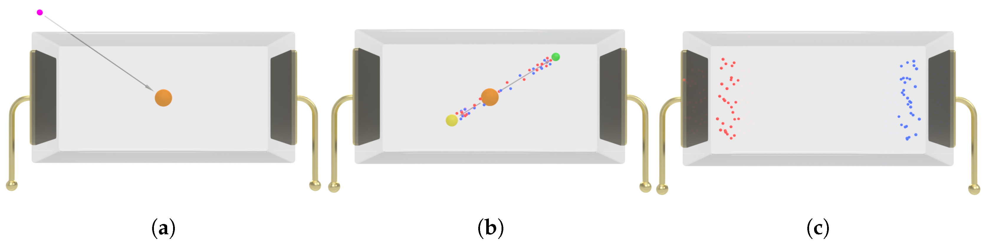
Detector grade lithium indium diselenide functions as a highly resistive, ohmic semiconductor. The primary detection mechanism for imaging is the thermal neutron absorption reaction Li(n,H)He with a 938 b thermal neutron cross section [17]. While the competing reaction In(n,)In maintains a thermal neutron cross section of 202 b, the secondary gamma has a high escape probability and has not been observed to affect significantly the neutron signal [16]. To enhance the thermal neutron capture efficiency of the sensor material, the lithium used for crystal synthesis is isotopically enriched to 95% Li [12,13]. When the incident neutron enters the bulk sensor material, it interacts via scattering or absorption as previously noted. Within this semiconducting material (band gap of 2.8 eV) the 4.78 MeV Q-value of the Li reaction creates a dense, localized region of electron-hole pairs as shown in Figure 1, given the low mean free path of the emitted triton and alpha particles [18].
Operating the sensor under a high voltage bias, the charge carriers are driven by the internal electric field of approximately 545 V/mm to opposing electrodes. In this material, the electron transport properties are significantly better than the corresponding hole transport properties, thus the signal pulse is primarily derived from the electron signal [19]. The induced charge at the electrode can be readily processed by the attached read out preamplifier or ASIC system.
1.4. High-Resolution Imaging
The Timepix ASIC, originally designed for position sensitive photon detection, is a proven platform for high resolution radiographic imaging. In past experiments, the device’s capabilities were extended from photon to neutron imaging by coupling the ASIC with a neutron sensitive conversion material, commonly LiF [20]. This scheme relies on detection in a silicon sub-layer to produce the charge signal event. Inherent issues arise due to particle transport distances within the conversion layer and detection layers, as well as pixel charge sharing. While careful design of the LiF conversion layer mitigates some of these effects, achieving fine spatial resolution, continually increasing layer thickness negatively impacts the detection efficiency [21].
The research detailed in this article further expands on the capabilities of direct charge readout, semiconductor neutron detectors through the adaptation of the LISe semiconductor neutron imager to the Timepix imaging ASIC. The LISe Timepix imager aims to provide a compact, low-power, lower-cost, high-resolution thermal neutron imaging system capable of achieving micron spatial resolution.
2. Materials and Methods
The LISe Timepix system demonstrates the application of a neutron sensitive semiconductor, mated to a high-resolution readout platform. The design utilizes single crystal lithium indium diselenide, enriched to 95% Li, as a direct band gap semiconductor capable of converting thermal neutron interactions to resolvable electronic charge.
2.1. Sensor Fabrication
The sensor material was grown as a single crystal boule, via the vertical Bridgman process, by the collaborators at Fisk University and Y-12 [22]. After dicing the boule, neutron sensitive regions of semiconductor grade crystal were selected to become LISe sensors [13]. To prepare the sensor for fabrication, the crystal was polished and etched in a 5% bromoethanol solution. This step removes any surface contamination and defects induced while polishing, enhancing contact adhesion during photolithography. The bulk sensor fabricated for this experiment measured 9.0 mm × 7.0 mm × 550 m.
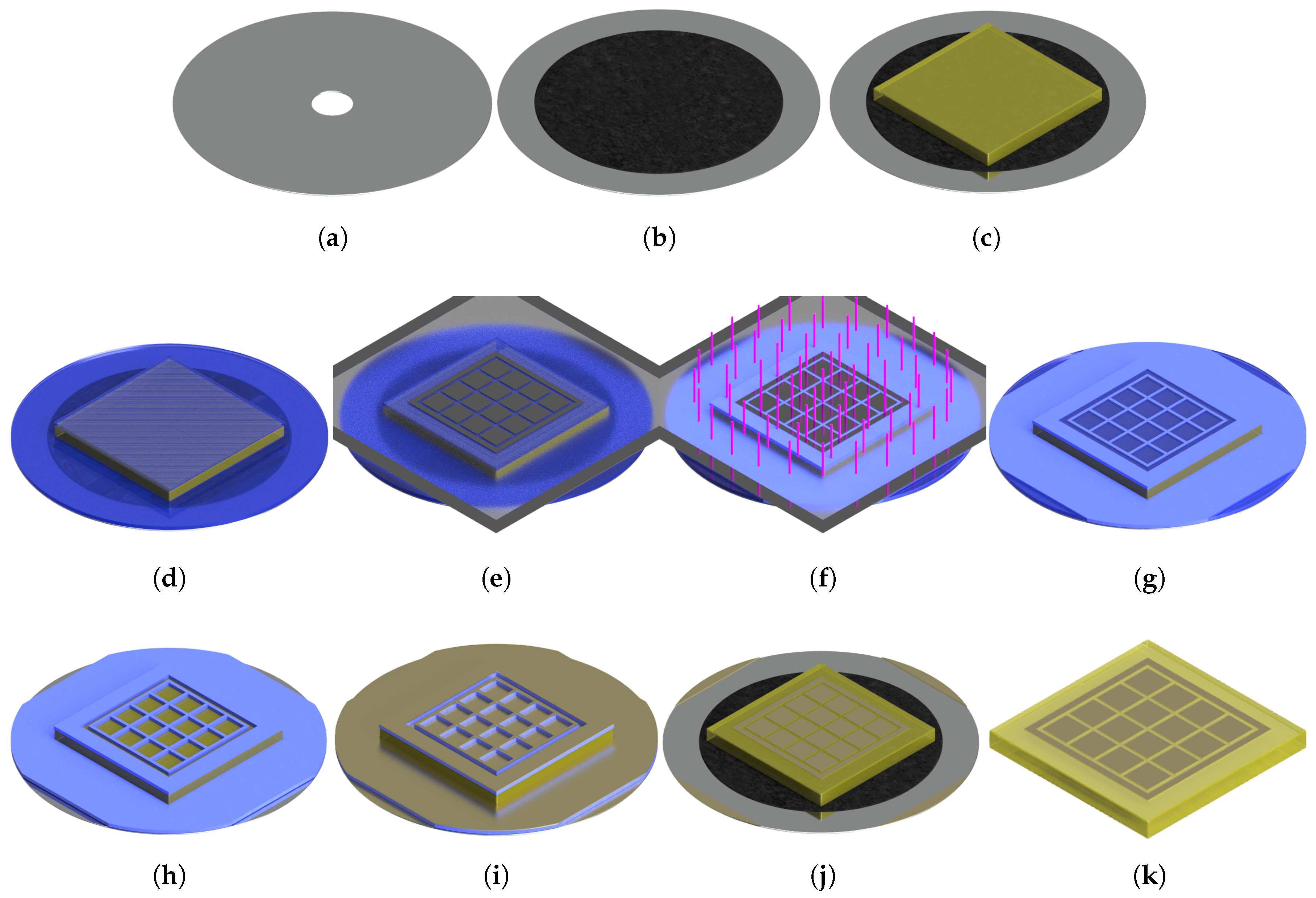
The photolithography process begins with a clean, stainless steel planchet as shown in Figure 2 (process depicts fabrication of the original 16-channel LISe pixel detector for simplicity [16]).
The planchet serves as a substitute wafer, conforming to the mechanical requirements for silicon based photolithography systems and allows indirect handling of the fragile LISe substrate. The sensor was bonded at temperature to the planchet using a chemically compatible bonding wax, suitable for ultra-high vacuum applications. Because both sides of a pixel detector required metallizing to fabricate electrodes, the wax also provides a protective base for the initial broad face contact. The mounted sensor was coated in Futurrex NR9-1000PY, a negative photoresist developed for layer lift-off. The sensor was aligned on a Karl Suss MA6 and exposed to UV radiation from an i-line Hg lamp (365 nm wavelength), transferring the photomask design to the photoresist. After developing the negative photoresist, the bare LISe substrate was exposed where electrodes would be deposited. Gold contact layers were sputtered onto the sensor using an AJA International confocal sputtering system outfitted with an 2 RF magnetron sputtering gun. The metal thickness measured 125 nm on the broad face side (single large pixel) and 100 nm on the pixelated side. In the final lift-off sequence, the excess metal was released from the patterned sensor, and the wax was dissolved to release the sensor from the planchet [3,23].
2.2. Imaging Device Construction
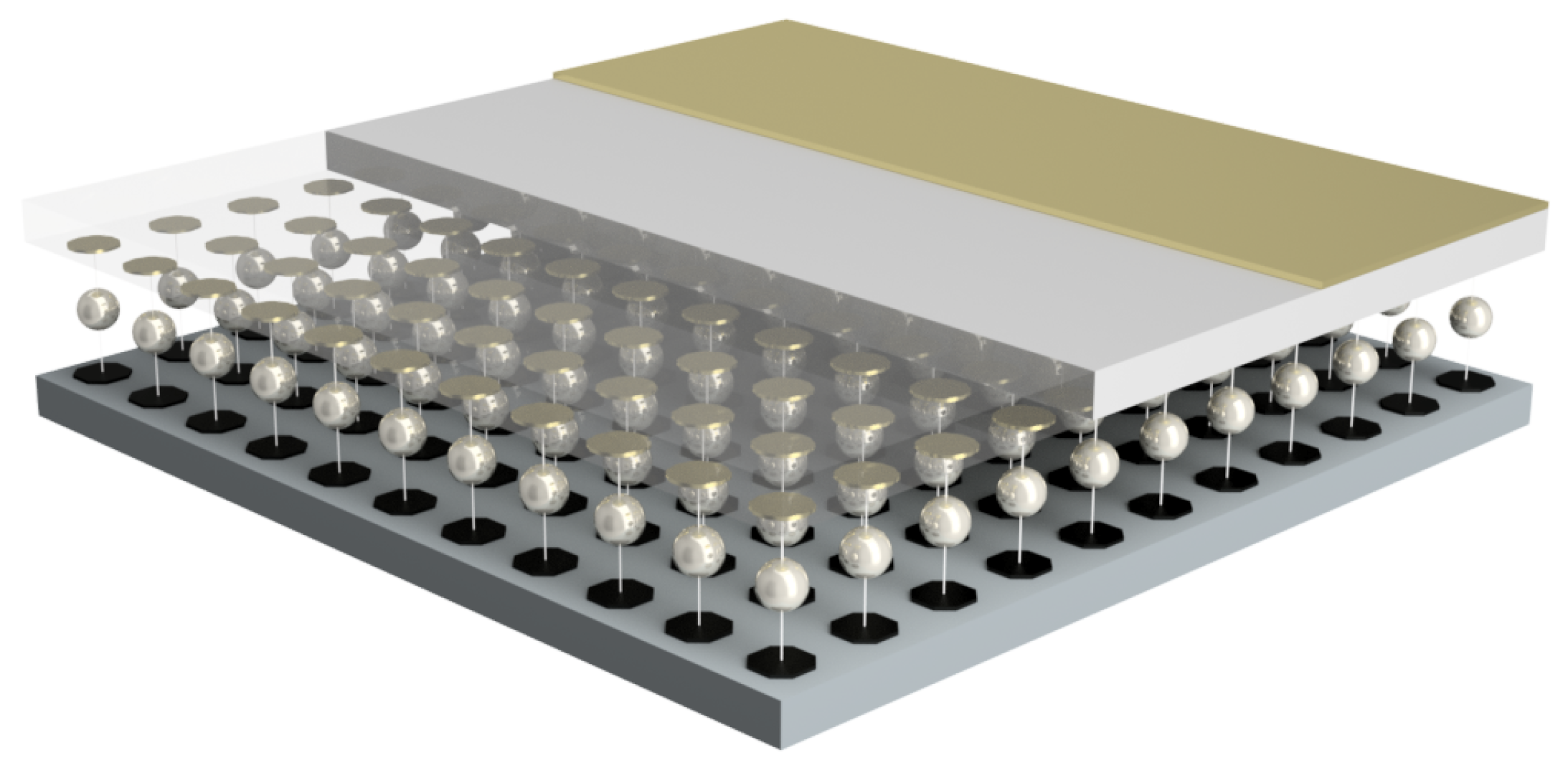
The LISe sensor fabrication parameters were tailored to accommodate the Timepix ASIC. The photomask used to pattern the LISe Timepix sensor featured a full pixels array of 30 m diameter, circular pixels at a 55 m pitch. This shape and diameter was selected to facilitate bonding with the Timepix ASIC along with minimizing charge sharing and breakdown between adjacent channels. The layering diagram is shown in Figure 3 (starting from the bottom): the Timepix ASIC substrate, the 30 m exposed bonding surface (octagonal), the 35 m indium bump balls, the 30 m gold pixels, the LISe sensor bulk and the gold broadface contact.
Presently limited by the crystal boule growth diameter, the sensor did not cover the entirety of the Timepix ASIC, omitting the guard ring in this design. The LISe sensor was flip-chip bump bonded to the Timepix ASIC, shown in Figure 4, by the former readout manufacturer X-ray Imatek (Barcelona, Spain).
The detection module consists of the LISe sensor, Timepix ASIC, and readout PCB encased in an aluminum enclosure. This module operates within the neutron beam, transmitting the detected neutron event to the remotely located readout module via ribbon cable. The low-power device accomplishes room temperature operation without requiring additional cooling under extended operation at the HFIR beamline.
2.3. HFIR Beamline Testing
As with previous iterations of the LISe neutron detection systems, performance experiments were conducted at HFIR at Oak Ridge National Laboratory (ORNL). Calibration and testing proceeded on the CG-1D beamline as well as some preliminary exposures using the CG-1A beamline to confirm device operation. Testing included open beam performance, edge sharpness measurement, resolution limit testing, and feature detection. Open beam images were used to eliminate inhomogeneities by dividing out the open beam signal from the attenuated image signal. The dark field images were also subtracted, however the dark current was minimal across the successfully bonded channels. The knife-edge test using a borated aluminum slit subjected the sensor to an abrupt change in neutron flux, permitting the usage of the modulation transfer function method to calculate edge resolution.
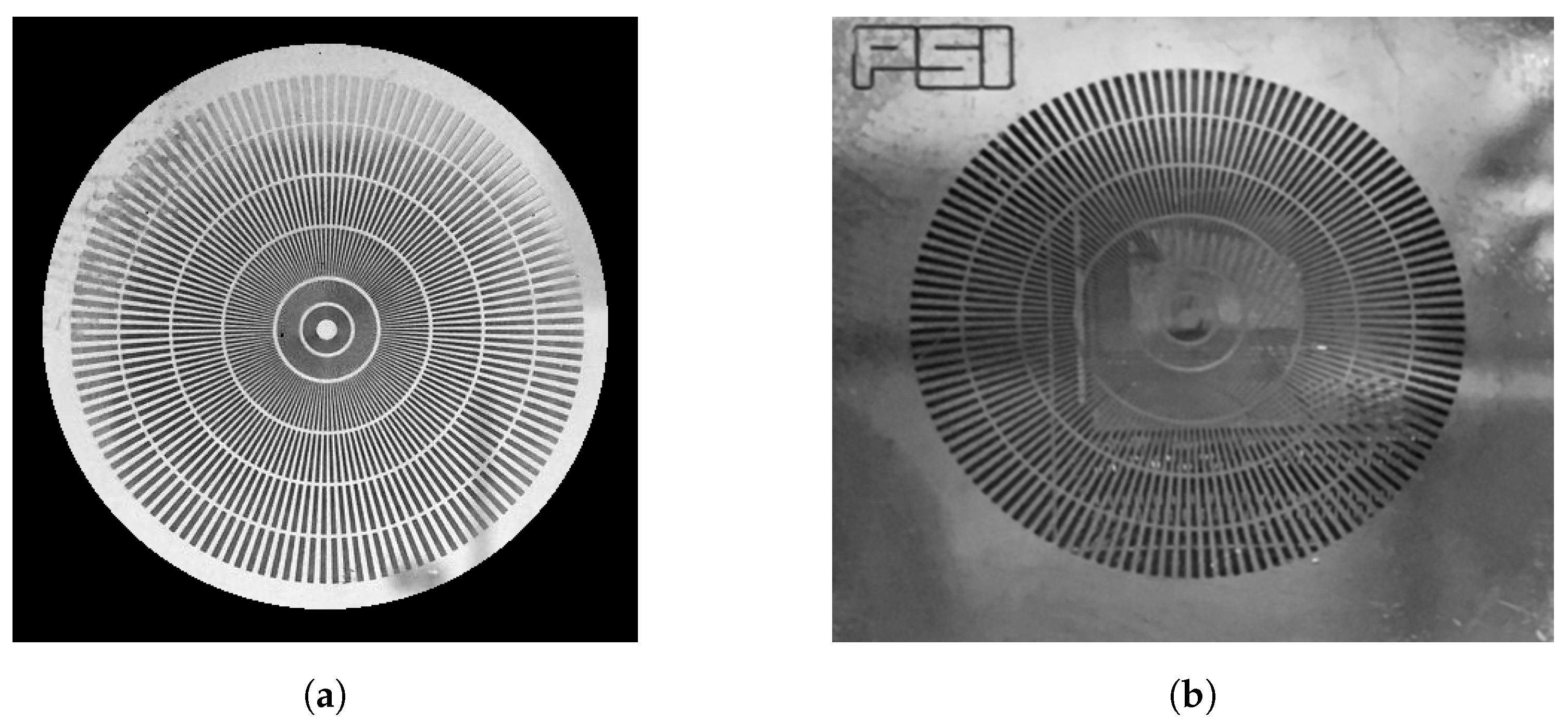
The Siemens star neutron imaging test mask was designed to visually quantify the resolution of thermal neutron imagers. The quartz mask was coated with a thin layer of Gd, a thermal neutron absorber, creating a uniform, geometric attenuation pattern for observation by the experimental device [24]. Figure 5 shows the PSI mask suspended over the LISe Timepix imager sensor and ASIC.
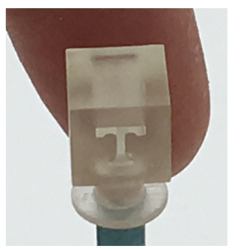
Along with resolution tests, the LISe imager was used to capture images of standardized samples for feature detection, mimicking applications in nuclear image analysis. In previous testing, the University of Tennessee “Power T” logo was captured using a standard 50 m thick LiF scintillating screen and a 650 m thick single crystal LISe scintillator for neutron imaging comparison [14]. The Power T imaging target (shown in Figure 6) was printed on a Formlabs Form 2 printer using SLA additive manufacturing [25,26].
The material selected was the Formlabs v2 Clear Resin photopolymer printed with the highest resolution settings, at 140 m spot size and 25 m layer thickness. The cube measured 1.0 cm to a side with the “Power T” logo inscribed the full depth of the cube. The top of the “Power T” measures approximately 600 m in length. The design permits neutrons to pass through the void inscribed in the cube, creating a negative image of the logo.
The CG-1D cold neutron beamline maintains a flux of approximately (∼10 n/cm/s) [5,27]. The colder spectrum thermal neutrons range in energy from 0.8 Ȧ to 6 Ȧ (peak ∼2.6 Ȧ). The 16 mm aperture was used in the beam configuration for this experiment at a distance of 6.6 m from the detector [28]. The neutron imaging targets were suspended between the LISe Timepix imager and the helium filled neutron flight tube. The LISe sensor detection plane was position approximately 7 mm and 15 mm behind the PSI mask and Power T target (beam L/D = 943:1 and 440:1), respectively. The proximity was limited by the enclosure and geometry of the support structures retaining the targets.
2.4. Image Processing
The Timepix readout electronics produced a 16-bit, time-stamped, binary data file for each frame captured by the system. Operating the device in counting mode, the frame acquisition window timing was adjusted to resolve the imaging target, while minimizing the number of saturated pixels. By capturing multiple frames, the series could be averaged to produce an image with increased contrast while minimizing hot pixels from background radiation or electrical noise. Even in a high-flux neutron beam, the small pixel area ( cm) prohibitively limits the neutron interaction rate. Because the system was a prototype, an arbitrarily large number of images were captured in each series based on the anticipated contrast, image complexity and allotted beam time. This approach helped to ensure adequate averaging could be applied in post processing to generate higher fidelity images post beam time. The white field images from the PuBe source and HFIR open beam have been presented as the raw series average, with the 16-bit data scaled between zero and unity. Dark field subtraction was implemented, although the signal was minimal due to low leakage current across each functional channel. The target images, scaled in the same fashion, were normalized to the open beam to remove some of the inhomogeneities.
3. Results
The LISe Timepix functioned successfully as a proof of concept prototype. There were some concerns as to the performance of the device due to sample limitations. Because the sensors were grown to a diameter smaller than the Timepix ASIC, the sensor only operated across a subset of the available channels. Without the ability to utilize a true guard ring around the sensor edge, the channels nearest the extremities exhibited tapered response. Guard rings are known to prevent edge breakdown in sensors operating under large internal electric fields [29]. The effective active area of the system covers approximately 150 × 100 pixels or 8.25 mm × 5.50 mm. Some channels were also non-responsive due to bond failures and/or crystalline defects, likely arising from incompatibilities in the flip-chip bump bonding process equipment. The result of these non-responsive channels manifests as the dead area in the upper right hand corner of the neutron images. This semiconductor LISe sensor exhibited a response edge, visible as the curved intensity variation, also observed in prior experiments utilizing LISe as a scintillator [15]. While this phenomena persists, this characteristic has only been present in some sensors and will require more crystal growth and testing to evaluate the primary mechanism. Despite this inconsistency, both regions are capable of responding to neutrons and producing images in under scintillator or semiconductor operational modes.
3.1. PuBe Source Response
After fabrication, the imager was tested at The University of Tennessee using a 2 mCi plutonium beryllium (PuBe) neutron source. The isotropic PuBe source emits approximately n/s, requiring an extended exposure time spanning 150 frames, each at 10 min acquisition window. The data was compiled to yield the final images shown in Figure 7.
The preliminary counting sample was conducted in two configurations, one with the PuBe source in a thermalizing, polyethylene enclosure and the other with the bare source directly exposed to the imager. The LISe Timepix imager showed a clear response to moderated PuBe source neutrons, while showing a diminished response to the unmoderated source as expected. While simulations show a decrease in total interaction cross-section for higher neutron energies by approximately a factor of 1000 [18], the fluxes are different due to the moderating enclosure, and would require a more in depth simulation and calibration experiment. The region of interest (ROI) shown for the thermalized response measured a mean intensity value of 0.0014 ± 0.00049. As a qualitative assessment, the sensor responds to a range of neutron energies, however the isotopic enrichment of Li enhances the detection efficiency of the LISe sensor at thermal energies.
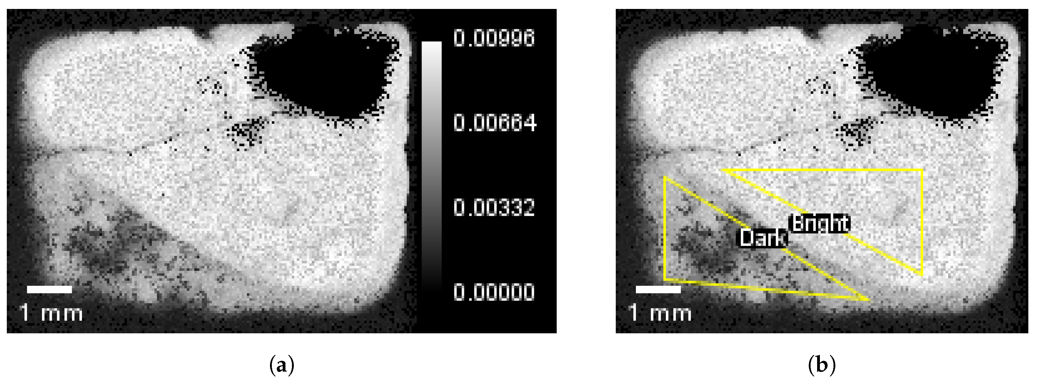
3.2. Open Beam Response
At the HFIR beamline, the initial experiment focused on calibrating the ASIC set points (acquisition window timing, bias voltage and threshold values) and obtaining a quality open beam image to serve as a reference. In the activated LISe sensor, the decay of In will release betas (isomer with a large end-point energy of 3.3 MeV) and the ground state (an end point energy of 1 MeV) where the branching ratio is 0.267 [14].The interaction rate compared to Li is dependent on the incident neutron energy, approximately 20% for this experiment. Therefor the higher isomer decay energy will manifest itself around 4% of the time in all neutron interactions. The range of a beta at this energy is 6 mm [18], over 100 times the pixel pitch, greatly distributing the charge. In this beam, the active imaging area saw a neutron fluence of approximately n/s, or roughly 300 n/s across each pixel. By selecting the correct threshold, these effects were not observable in the images with the large neutron flux.
As previously mentioned, Figure 8 demonstrates the curved response phenomena, now more clearly defined by the higher flux beam.
The mean intensity value for the dark ROI measured 0.0052 ± 0.00178 with the bright ROI measuring 0.0086 ± 0.0008. This corresponds to a 40% decrease in signal output across the transition from the bright region to dark region. As the exact mechanism behind this phenomena is still unknown, it is uncertain as to the degree of variation expected along the transition without prior measurement with the specific device. The open beam response demonstrated less variation in light intensity than the PuBe source, likely attributed to a more narrow neutron energy spectrum and optimized geometry. Also visible is the full, rectangular active area, made possible by the significantly increased neutron flux. This image was created from 50 frames at a 1 s acquisition window. For these experiments, the high-voltage supplied by the readout module was fixed at +300 V.
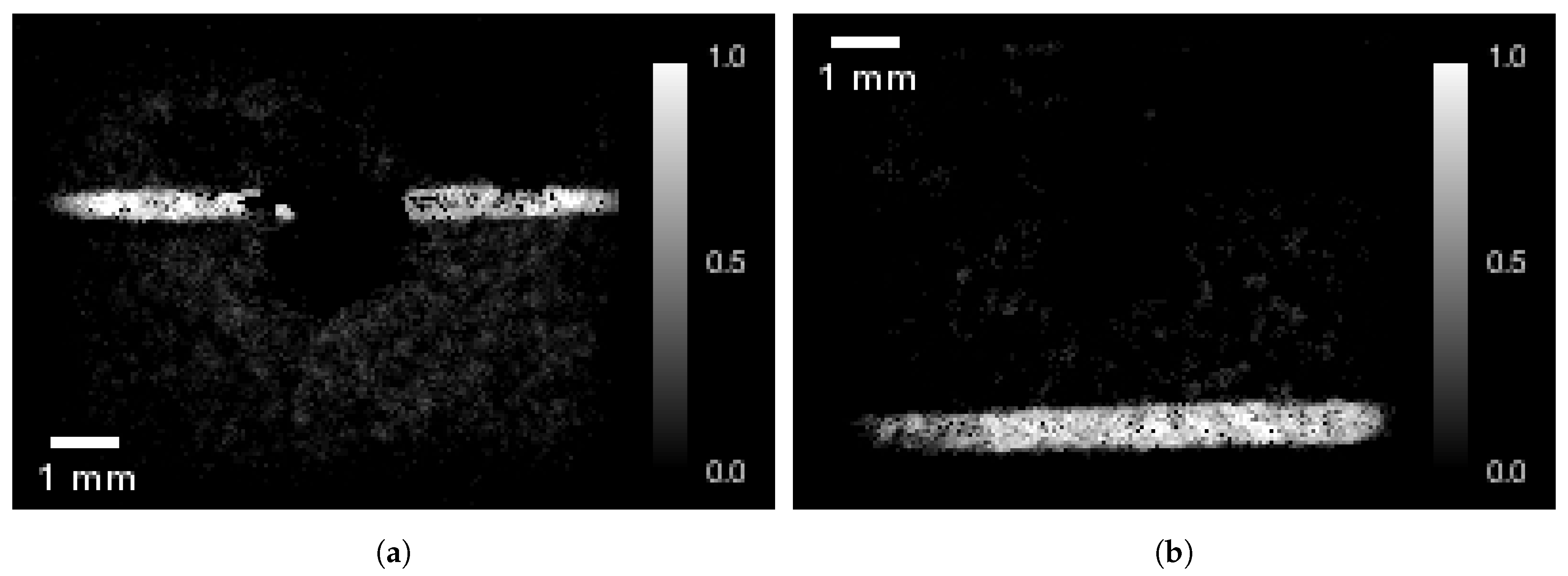
3.3. Knife Edge Test
The knife edge test subjects the imager to an abrupt change in incident neutron flux. By blocking off part of the neutron beam, an edge is created along the imaging plane, directly contrasting the response to open beam and attenuated conditions. A 1/16th inch thick aluminum sheet with borated coating was placed in front of the LISe Timepix imager, at a distance of roughly 10 mm (beam L/D = 660:1). The sheet featured long thin slits (500 m and 750 m) running horizontally across the metal (as milled). Each image was generated from a set of 50 frames at 1 s acquisitions; in both cases, the results showed a clear band as illustrated in Figure 9.
The band across the imaging plane represents the unobstructed neutron beam. The 550 m slit is broken in the middle due to dead pixels, otherwise maintaining uniform intensity across the horizontal axis. The 750 m slit shows a decrease in brightness in the lower left corner of the sensor, corresponding to the material response phenomena.
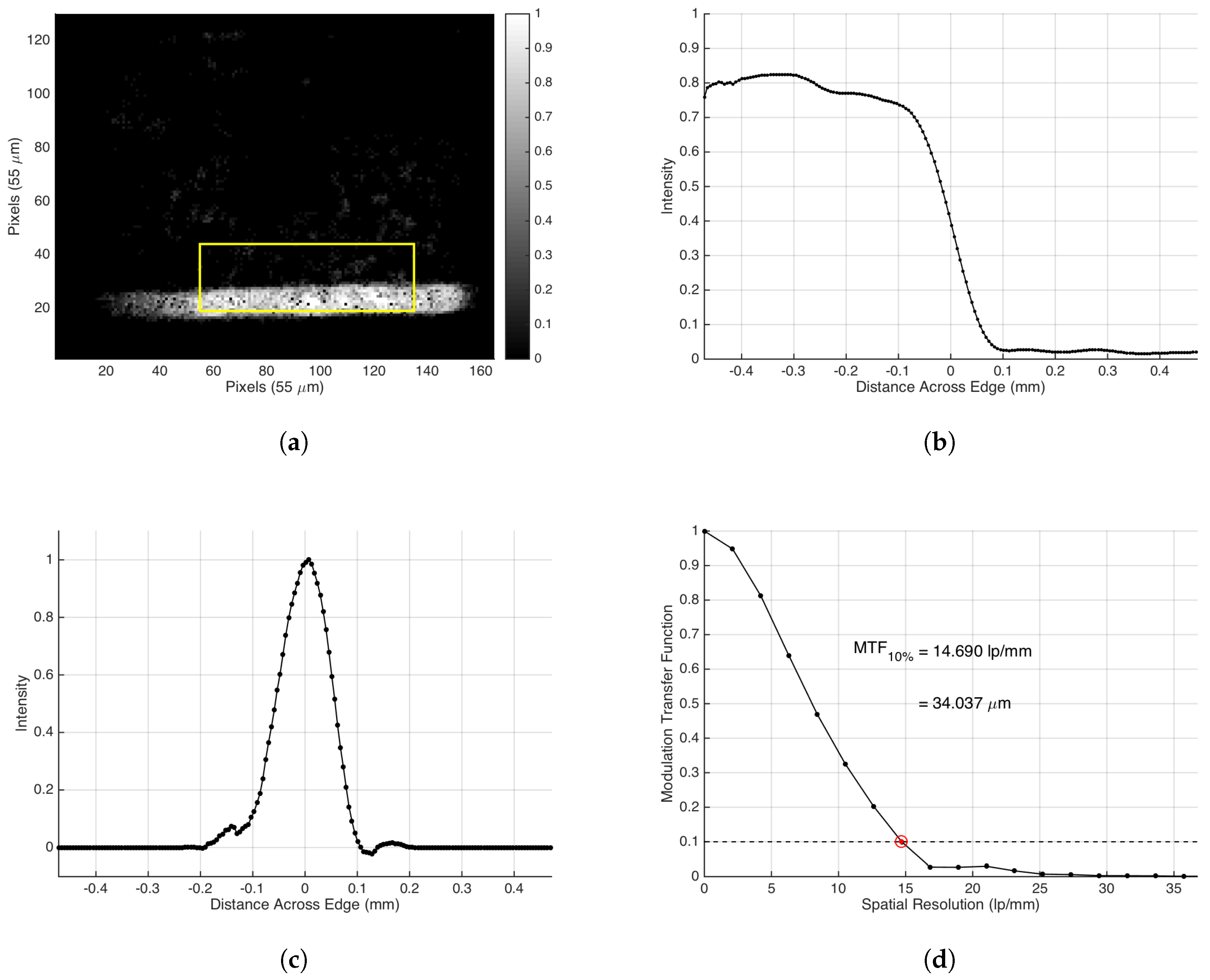
To characterize the edge sharpness and image contrast, the modulation transfer function method [15] was employed across the 750 m slit band. The region of interest extended 80 pixels in the band direction, spanning a width of 25 pixels across the edge profile, as shown by the yellow ROI in Figure 10.
The edge spread function (ESF) demonstrates the contrast between the open beam and the attenuated signal transmitted through the cadmium sheet. The knife edge was aligned at a small offset angle from horizontal to remove the pixel size limit imposed on the spatial resolution. The Canny edge detection method created a binary line image, evaluated using the Hough Transform to produce an edge angle of roughly (2°). The edge angle was then implemented to align the edge spread functions for each column, forming a single averaged ESF. The ESF was differentiated to create the line spread function (LSF), and a Gaussian fit yielded the peak center offset. After centering the LSF, a modified Hann window was applied (Tukey window with and half the LSF width), reducing noise from the signal edges [30]. The LSF was then converted to the frequency domain using a fast Fourier transform. The modulation transfer function was mapped to determine the effective line pair resolution parameter, evaluated at the 10% limit, yielding 14.7 lp/mm or a resolution value of roughly 34 m. The calculated resolution value was approximately 2/3 the pixel pitch as tested in this experiment.
3.4. Resolution Testing
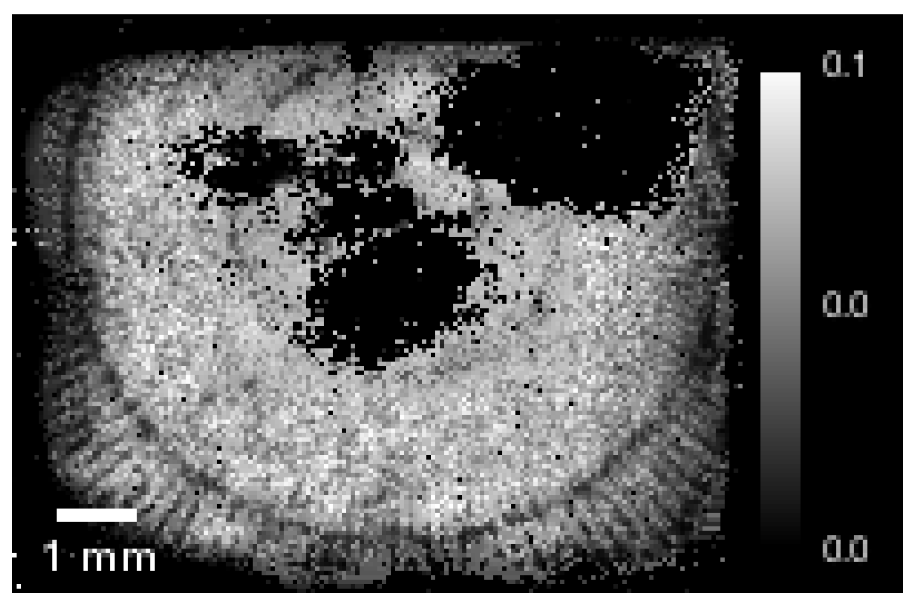
The PSI mask was captured with the LISe Timepix imager to determine the ultimate resolution of the device. To generate this image, 400 frames at 1 s acquisition intervals were obtained at a distance of approximately 7 mm from the sensor. The outer ring visible in Figure 11 corresponds to the 200 m line pair spacing.
The indicator ring itself can clearly be seen circumventing the bottom half of the imager. Some of the line pairs are resolvable going further in to the center of the PSI mask, indicating the resolution may be finer than 200 m, with refined sensor packaging and optimized acquisition parameters.
3.5. Object Identification
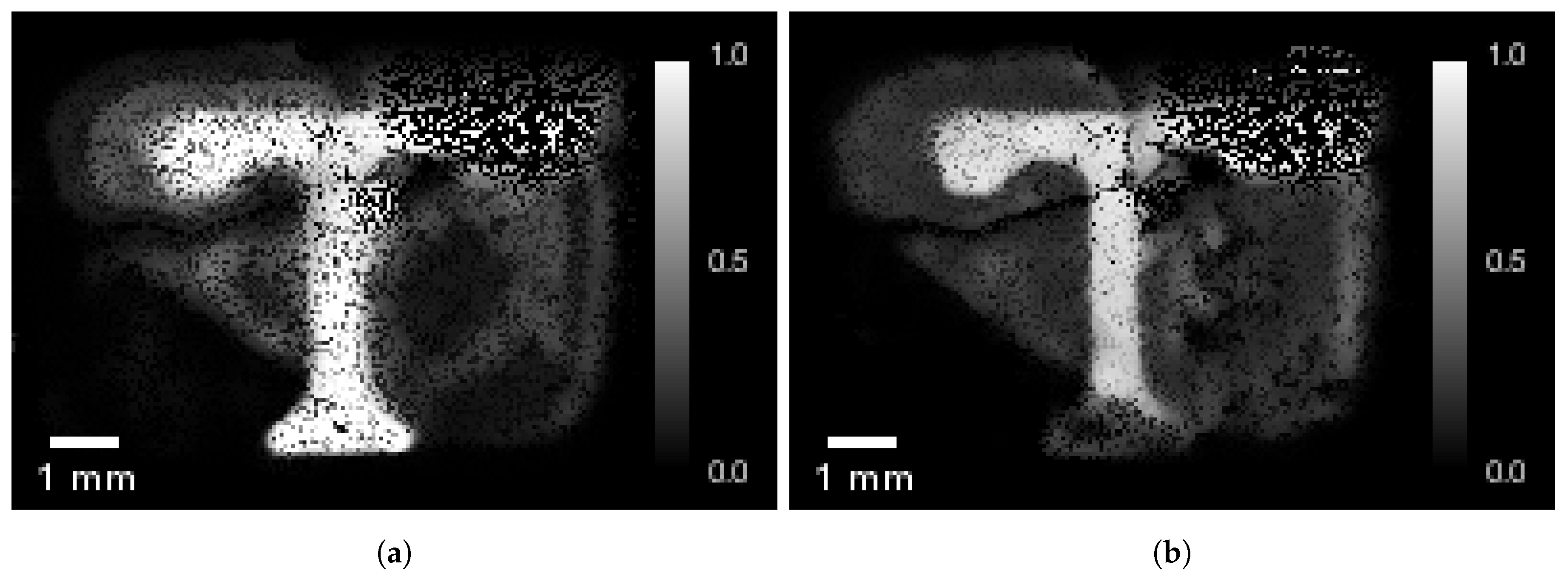
Object identification requires the accurate assessment of unknown features within an inaccessible object. Calibrating the systems operational parameters can help clarify features under investigation, as shown in Figure 12.
Both images were built from 50 frames at 10 s acquisition intervals. These images were conducted later in the experiment after acquisition parameters were refined and a suitable upper threshold discrimination value was selected. The lower threshold image (+4 mV) does not show as stark of contrast as compared the higher threshold image (+24 mV). The lower threshold allows the less responsive corner area to partially resolve the foot of the “T”, and is more forgiving along the crystal defects. However, the higher threshold shows sharper edges in the top of the letter, more closely resembling the actual part.
4. Discussion
The LISe Timepix imaging system performed admirably as a first prototype. The device responded to a range of cold and thermal neutrons as well as some higher energy neutron spectra from a PuBe source. Using 95% Li enriched lithium indium diselenide provided enhanced neutron detection efficiency, offering both qualitative and quantitative results. While the active sensor area was limited by crystal response inhomogeneities from intrinsic defects, and coupling to the Timepix ASIC, the usable pixels provided a relatively uniform open beam, and fortified confidence in this technology. Using quantitative assessment, the device edge resolution was validated at 34 m. The technology shows great potential to go even smaller using techniques such as charge centroiding and super sampling with a step size smaller than the 55 m pixel pitch. The acquisition times rivaled the previous LISe scintillator imaging experiments [14,15], generally requiring 1 second to acquire a single frame and between 1 to 10 minutes to capture high resolution images, given neutron flux at HFIR. Furthermore, the system ran continuously under neutron flux at HFIR for a period of roughly 3 days, capturing data without degradation in sensor performance.
Qualitatively, the image resolution was estimated to <200 m using the PSI Seimens star mask, again limited by positioning and device performance. However, visible inspection of the “Power T” clearly indicates the device was able to resolve features on the order of the pixel pitch. Using post processing techniques, such as super sampling, may further increase the achievable resolution for this imager configuration. By imaging a 3D modeled part made on an SLA printer, this device demonstrates the ability to accomodate forward looking technologies and associated investigatory techniques. Further applications will extend to imaging of hydrogenous materials in biological systems as well as special nuclear materials for national security.
5. Conclusions
This experiment successfully demonstrated the feasibility of lithium indium diselenide coupled with the Timepix ASIC. While the sensor is still in the prototype phase, the material demonstrated compatibility with the pre-exisiting readout ASIC, and with further tuning, can produce a high fidelity, direct readout semiconductor neutron detector. The neutron detection efficiency can reach 87% for 1.0 mm thick sensors subjected to 3.297 neutrons [18], which is currently possible with the present synthesis techniques. The high absorption efficiency has the added benefit of shielding the underlying ASIC, creating a device suitable for sustained, high flux, thermal neutron environments [18].
More work should be conducted to optimize the LISe sensor to Timepix ASIC bonding along with tuning the system for the specific beamline and target configurations. With optimized operational parameters, the acquisition time should be reduced while also increasing the resolution of the imager. However, it should be noted that the presence of In limits the detectable interaction rate to 79% of the absorption rate, governing the maximum efficiency possible for LISe. Future development avenues include the realization of a complete LISe Timepix neutron imager (with the full field of view), via growing a larger single crystal boule, capable of spanning the entire ASIC, or the tiling of multiple sensors across a single ASIC. To increase the active imaging area, it would also be possible to tile multiple LISe Timepix systems together, as seen in the Widepix detector for x-ray imaging [31].
Acknowledgments
This work is supported through subcontract number 4300090406 from CNS Y-12 National Security Complex and this material is based upon work supported under a Department of Energy Nuclear Energy University Programs Graduate Fellowship. A portion of this research at ORNL’s High Flux Isotope Reactor was sponsored by the Scientific User Facilities Division, Office of Basic Energy Sciences, U.S. Department of Energy.
Author Contributions
Elan Herrera, Eric Lukosi, Ashley Stowe and Jeffrey Preston conceived and designed the experiments; Ashley Stowe developed the lithium purification and sensor growth process; Brenden Wiggins and Arnold Burger conducted the physical growth of the sensor material; Ashley Stowe and Jeffrey Preston supplied sensor material; Elan Herrera and Daniel Hamm processed sensors and fabricated the imaging system; Elan Herrera and Eric Lukosi performed the beamline experiments; Elan Herrera analyzed the data; Elan Herrera wrote the paper.
Conflicts of Interest
The authors declare no conflict of interest. Furthermore, the founding sponsors had no role in the design of the study; in the collection, analyses, or interpretation of data; in the writing of the manuscript, and in the decision to publish the results.
Abbreviations
The following abbreviations are used in this manuscript:
| ASIC | Application specific integrated circuit |
| CAD | Computer aided design |
| DOAJ | Directory of open access journals |
| RF | Radio frequency |
| HFIR | High-Flux Isotope Reactor |
| LISe | Lithium indium diselenide |
| MDPI | Multidisciplinary Digital Publishing Institute |
| ORNL | Oak Ridge National Laboratory |
| PCB | Printed circuit board |
| PSI | Paul Scherrer Institute |
| ROI | Region of interest |
| SLA | Stereolithography apparatus |
| UV | Ultraviolet |
References
- Anderson, I.S.; Bilheux, H.Z.; McGreevy, R. (Eds.) Neutron Imaging and Applications; Springe: New York, NY, USA, 2009. [Google Scholar]
- Grünzweig, C.; Mannes, D.; Kaestner, A.; Schmid, F.; Vontobel, P.; Hovind, J.; Hartmann, S.; Peetermans, S.; Lehmann, E. Progress in Industrial Applications using Modern Neutron Imaging Techniques. Phys. Procedia 2013, 43, 231–242. [Google Scholar] [CrossRef]
- Owens, A. Compound Semiconductor Radiation Detectors; CRC Press: Boca Raton, FL, USA, 2016. [Google Scholar]
- Baker, C.; Green, K.; van der Grinten, M.; Iaydjiev, P.; Ivanov, S.; Al-Ayoubi, S.; Harris, P.; Pendlebury, J.; Shiers, D.; Geltenbort, P. Development of solid-state silicon devices as ultra cold neutron detectors. Nucl. Instrum. Methods Phys. Res. Sect. A Accel. Spectrom. Detect. Assoc. Equip. 2002, 487, 511–520. [Google Scholar] [CrossRef]
- Santodonato, L.; Bilheux, H.; Bailey, B.; Bilheux, J.; Nguyen, P.; Tremsin, A.; Selby, D.; Walker, L. The CG-1D Neutron Imaging Beamline at the Oak Ridge National Laboratory High Flux Isotope Reactor. Phys. Procedia 2015, 69, 104–108. [Google Scholar] [CrossRef]
- Trtik, P.; Hovind, J.; Grünzweig, C.; Bollhalder, A.; Thominet, V.; David, C.; Kaestner, A.; Lehmann, E.H. Improving the Spatial Resolution of Neutron Imaging at Paul Scherrer Institut—The Neutron Microscope Project. Phys. Procedia 2015, 69, 169–176. [Google Scholar] [CrossRef]
- Trtik, P.; Lehmann, E.H. Progress in High-resolution Neutron Imaging at the Paul Scherrer Institut—The Neutron Microscope Project. J. Phys. Conf. Ser. 2016, 746, 012004. [Google Scholar] [CrossRef]
- Tremsin, A.S.; Feller, W.B.; Downing, R.G. Efficiency optimization of microchannel plate (MCP) neutron imaging detectors. I. Square channels with 10B doping. Nucl. Instrum. Methods Phys. Res. Sect. A Accel. Spectrom. Detect. Assoc. Equip. 2005, 539, 278–311. [Google Scholar] [CrossRef]
- Tremsin, A.; Morgano, M.; Panzner, T.; Lehmann, E.; Filgers, U.; Vallerga, J.; McPhate, J.; Siegmund, O.; Feller, W. High resolution neutron imaging capabilities at BOA beamline at Paul Scherrer Institut. Nucl. Instrum. Methods Phys. Res. Sect. A Accel. Spectrom. Detect. Assoc. Equip. 2015, 784, 486–493. [Google Scholar] [CrossRef]
- Tremsin, A.; Vallerga, J.; McPhate, J.; Siegmund, O. Optimization of high count rate event counting detector with Microchannel Plates and quad Timepix readout. Nucl. Instrum. Methods Phys. Res. Sect. A Accel. Spectrom. Detect. Assoc. Equip. 2015, 787, 20–25. [Google Scholar] [CrossRef]
- Tupitsyn, E.; Bhattacharya, P.; Rowe, E.; Matei, L.; Groza, M.; Wiggins, B.; Burger, A.; Stowe, A. Single crystal of LiInSe2 semiconductor for neutron detector. Appl. Phys. Lett. 2012, 101. [Google Scholar] [CrossRef]
- Stowe, A.; Woodward, J.; Tupitsyn, E.; Rowe, E.; Wiggins, B.; Matei, L.; Bhattacharya, P.; Burger, A. Crystal growth in LiGaSe2 for semiconductor radiation detection applications. J. Cryst. Growth 2013, 379, 111–114. [Google Scholar] [CrossRef]
- Tupitsyn, E.; Bhattacharya, P.; Rowe, E.; Matei, L.; Cui, Y.; Buliga, V.; Groza, M.; Wiggins, B.; Burger, A.; Stowe, A. Lithium containing chalcogenide single crystals for neutron detection. J. Cryst. Growth 2014, 393, 23–27. [Google Scholar] [CrossRef]
- Lukosi, E.; Herrera, E.; Hamm, D.; Lee, K.M.; Wiggins, B.; Trtik, P.; Penumadu, D.; Young, S.; Santodonato, L.; Bilheux, H.; et al. Lithium indium diselenide: A new scintillator for neutron imaging. Nucl. Instrum. Methods Phys. Res. Sect. A Accel. Spectrom. Detect. Assoc. Equip. 2016, 830, 140–149. [Google Scholar] [CrossRef]
- Lukosi, E.D.; Herrera, E.H.; Hamm, D.S.; Burger, A.; Stowe, A.C. Neutron imaging with lithium indium diselenide: Surface properties, spatial resolution, and computed tomography. Nucl. Instrum. Methods Phys. Res. Sect. A Accel. Spectrom. Detect. Assoc. Equip. 2017, 872, 181–186. [Google Scholar] [CrossRef]
- Herrera, E.; Hamm, D.; Wiggins, B.; Milburn, R.; Burger, A.; Bilheux, H.; Santodonato, L.; Chvala, O.; Stowe, A.; Lukosi, E. LISe pixel detector for neutron imaging. Nucl. Instrum. Methods Phys. Res. Sect. A Accel. Spectrom. Detect. Assoc. Equip. 2016, 833, 142–148. [Google Scholar] [CrossRef]
- Knoll, G.F. Radiation Detection and Measurement; John Wiley & Sons: Hoboken, NJ, USA, 2010. [Google Scholar]
- Lukosi, E.; Chvala, O.; Stowe, A. Response functions of semiconducting lithium indium diselenide. Nucl. Instrum. Methods Phys. Res. Sect. A Accel. Spectrom. Detect. Assoc. Equip. 2016, 822, 9–14. [Google Scholar] [CrossRef]
- Hamm, D.S.; Lukosi, E.D.; Rust, M.R.; Herrera, E.H.; Burger, A.; Wiggins, B.; Stowe, A.C. Characterization of lithium indium diselenide. In Proceedings of the IEEE Nuclear Science Symposium and Medical Imaging Conference (NSS/MIC), San Diego, CA, USA, 31 October–7 November 2015. [Google Scholar]
- Jakubek, J.; Holy, T.; Lehmann, E.; Pospisil, S.; Uher, J.; Vacik, J.; Vavrik, D. Spatial resolution of Medipix-2 device as neutron pixel detector. Nucl. Instrum. Methods Phys. Res. Sect. A Accel. Spectrom. Detect. Assoc. Equip. 2005, 546, 164–169. [Google Scholar] [CrossRef]
- Jakubek, J.; Schmidt-Wellenburg, P.; Geltenbort, P.; Platkevic, M.; Plonka-Spehr, C.; Solc, J.; Soldner, T. A coated pixel device TimePix with micron spatial resolution for UCN detection. Nucl. Instrum. Methods Phys. Res. Sect. A Accel. Spectrom. Detect. Assoc. Equip. 2009, 600, 651–656. [Google Scholar] [CrossRef]
- Wiggins, B.; Groza, M.; Tupitsyn, E.; Lukosi, E.; Stassun, K.; Burger, A.; Stowe, A. Scintillation properties of semiconducting 6LiInSe2 crystals to ionizing radiation. Nucl. Instrum. Methods Phys. Res. Sect. A Accel. Spectrom. Detect. Assoc. Equip. 2015, 801, 73–77. [Google Scholar] [CrossRef]
- Ohring, M. Material Science of Thin Films: Deposition and Structure, 2nd ed.; Academic Press, Inc.: San Diego, CA, USA, 2001. [Google Scholar]
- Grünzweig, C.; Frei, G.; Lehmann, E.; Kühne, G.; David, C. Highly absorbing gadolinium test device to characterize the performance of neutron imaging detector systems. Rev. Sci. Instrum. 2007, 78. [Google Scholar] [CrossRef] [PubMed]
- Formlabs, Inc. ‘High Resolution SLA and SLS 3D Printers for Professionals’. 2017. Available online: https//www.formlabs.com (accessed on 26 September 2017).
- Gibson, I.; Rosen, D.W.; Stucker, B. Additive Manufacturing Technologies; Springer: New York, NY, USA, 2014. [Google Scholar]
- Bilheux, H.Z.; Bilheux, J.C.; Bailey, W.B.; Keener, W.S.; Davis, L.E.; Herwig, K.W.; Cekanova, M. Neutron imaging at the Oak Ridge National Laboratory: Application to biological research. In Proceedings of the 2014 IEEE Biomedical Sciences and Engineering Conference, Oak Ridge, TN, USA, 6–8 May 2014. [Google Scholar]
- Crow, L.; Robertson, L.; Bilheux, H.; Fleenor, M.; Iverson, E.; Tong, X.; Stoica, D.; Lee, W. The CG1 instrument development test station at the high flux isotope reactor. Nucl. Instrum. Methods Phys. Res. Sect. A Accel. Spectrom. Detect. Assoc. Equip. 2011, 634, S71–S74. [Google Scholar] [CrossRef]
- Rossi, L.; Fischer, P.; Rohe, T.; Wermes, N. Pixel Detectors: From Fundamentals to Applications; Springer: Berlin, Germany, 2006. [Google Scholar]
- Cao, R.L.; Biegalski, S.R. The measurement of the presampled MTF of a high spatial resolution neutron imaging system. Nucl. Instrum. Methods Phys. Res. Sect. A Accel. Spectrom. Detect. Assoc. Equip. 2007, 582, 621–628. [Google Scholar] [CrossRef]
- Jakubek, J.; Jakubek, M.; Platkevic, M.; Soukup, P.; Turecek, D.; Sykora, V.; Vavrik, D. Large area pixel detector WIDEPIX with full area sensitivity composed of 100 Timepix assemblies with edgeless sensors. J. Instrum. 2014, 9, C04018. [Google Scholar] [CrossRef]
Figure 1.
Neutron detection in lithium indium diselenide (LISe) semiconducting sensor. (a) incident neutron is absorbed by Li in semiconductor bulk; (b) emitted H and generate charged particle pairs; (c) charge carriers driven to electrodes by applied internal electric field.
Figure 1.
Neutron detection in lithium indium diselenide (LISe) semiconducting sensor. (a) incident neutron is absorbed by Li in semiconductor bulk; (b) emitted H and generate charged particle pairs; (c) charge carriers driven to electrodes by applied internal electric field.

Figure 2.
Photolithography process using negative resist for pixelated LISe semiconductor sensor fabrication (16-channel pixel detector with square pixels and guard ring [16] shown for demonstration). (a) clean planchet; (b) apply wax coating; (c) bond sensor; (d) spincoat and bake; (e) align photomask; (f) UV exposure; (g) post bake; (h) develop resist; (i) deposit metal; (j) lift-off resist; (k) clean final sensor.

Figure 3.
LISe Timepix layering diagram.

Figure 4.
LISe semiconductor coupled to Timepix readout chip. (a) CAD model of LISe Timepix detection module; (b) bonded LISe Timepix imager PCB .
Figure 4.
LISe semiconductor coupled to Timepix readout chip. (a) CAD model of LISe Timepix detection module; (b) bonded LISe Timepix imager PCB .
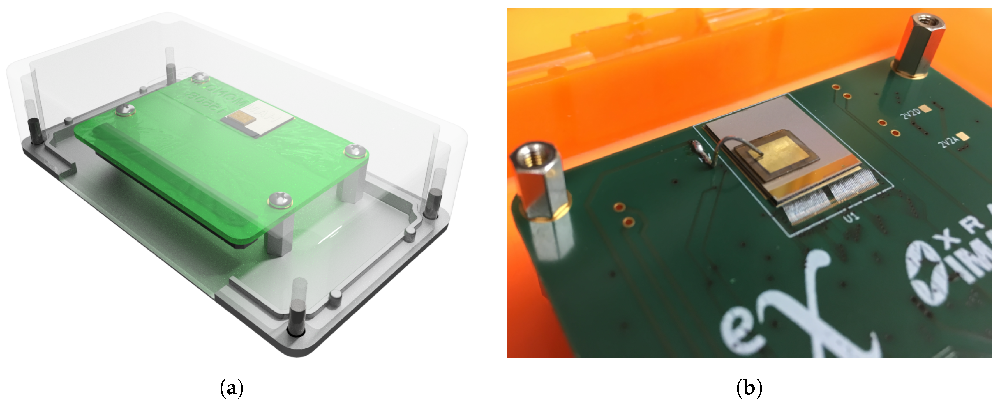
Figure 5.
PSI Siemens star neutron imaging resolution test target photographs [24]. (a) Siemens star photograph; (b) mask positioned in front of LISe Timepix for size comparison (image captured at an angle showing reflection off broad face contact).
Figure 5.
PSI Siemens star neutron imaging resolution test target photographs [24]. (a) Siemens star photograph; (b) mask positioned in front of LISe Timepix for size comparison (image captured at an angle showing reflection off broad face contact).

Figure 6.
Photograph of 3D printed “Power T” target.

Figure 7.
Neutron field response image to 2 mCi PuBe source. (a) thermalized PuBe source; (b) bare PuBe source; (c) thermalized PuBe source region of interest (ROI).
Figure 7.
Neutron field response image to 2 mCi PuBe source. (a) thermalized PuBe source; (b) bare PuBe source; (c) thermalized PuBe source region of interest (ROI).
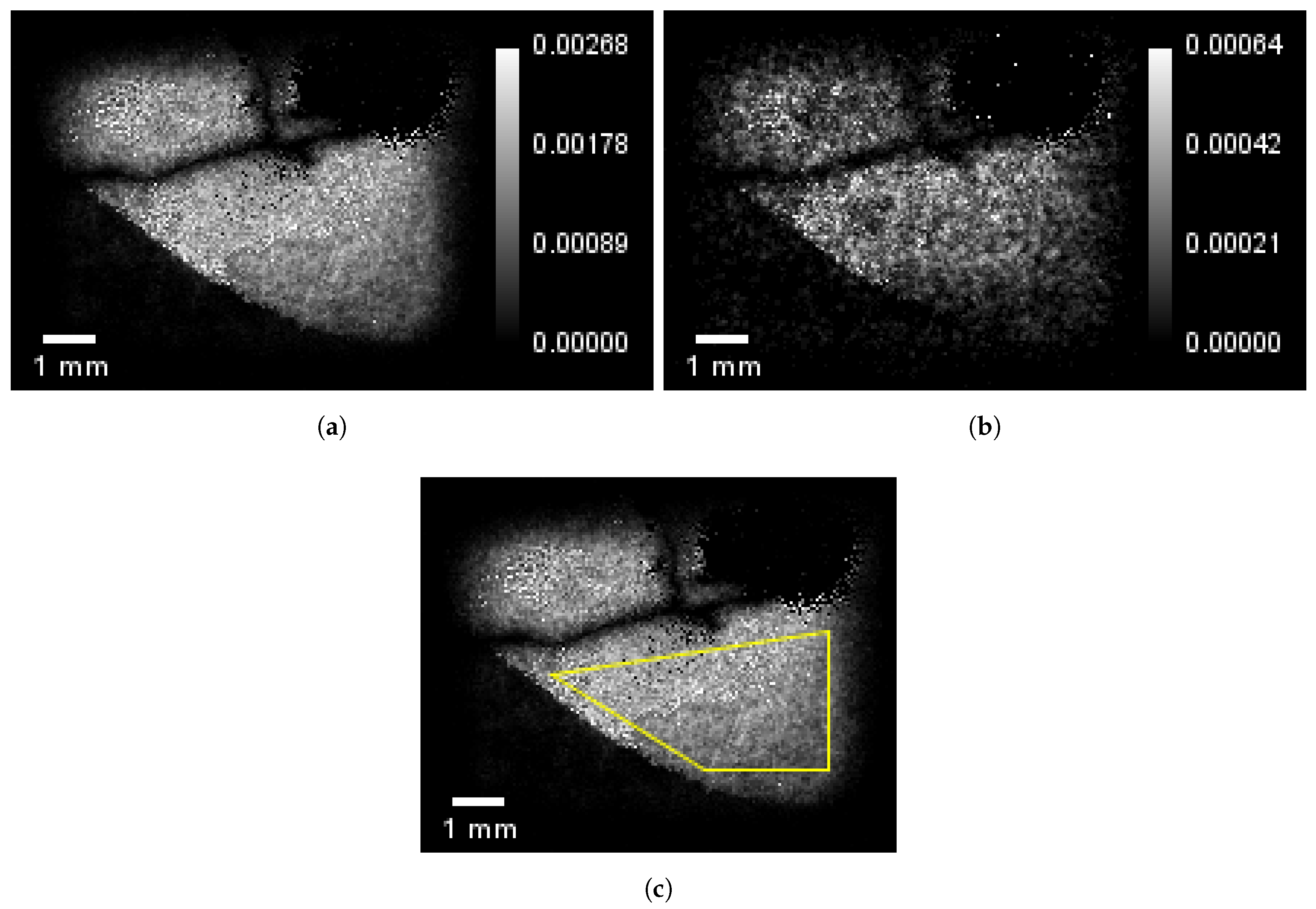
Figure 8.
HFIR CG-1D open beam neutron response image. (a) open beam response; (b) open beam intensity ROI.
Figure 8.
HFIR CG-1D open beam neutron response image. (a) open beam response; (b) open beam intensity ROI.

Figure 9.
Neutron image of knife edge slit in thin cadmium attenuating sheet. (a) slit: 500 m; (b) slit: 750 m.
Figure 9.
Neutron image of knife edge slit in thin cadmium attenuating sheet. (a) slit: 500 m; (b) slit: 750 m.

Figure 10.
Modulation transfer function method to calculate edge resolution. (a) 750 m slit with ROI overlay; (b) slit edge spread function; (c) slit line spread function; (d) slit modulation transfer function.
Figure 10.
Modulation transfer function method to calculate edge resolution. (a) 750 m slit with ROI overlay; (b) slit edge spread function; (c) slit line spread function; (d) slit modulation transfer function.

Figure 11.
Neutron image of Seimens star on PSI resolution test mask.

Figure 12.
Neutron image of 3D printed “Power T”. (a) threshold: +4 mV; (b) threshold: +24 mV.

© 2017 by the authors. Licensee MDPI, Basel, Switzerland. This article is an open access article distributed under the terms and conditions of the Creative Commons Attribution (CC BY) license (http://creativecommons.org/licenses/by/4.0/).
Share and Cite
MDPI and ACS Style
Herrera, E.; Hamm, D.; Stowe, A.; Preston, J.; Wiggins, B.; Burger, A.; Lukosi, E. Neutron Imaging with Timepix Coupled Lithium Indium Diselenide. J. Imaging 2018, 4, 10. https://doi.org/10.3390/jimaging4010010
AMA Style
Herrera E, Hamm D, Stowe A, Preston J, Wiggins B, Burger A, Lukosi E. Neutron Imaging with Timepix Coupled Lithium Indium Diselenide. Journal of Imaging. 2018; 4(1):10. https://doi.org/10.3390/jimaging4010010
Chicago/Turabian StyleHerrera, Elan, Daniel Hamm, Ashley Stowe, Jeffrey Preston, Brenden Wiggins, Arnold Burger, and Eric Lukosi. 2018. "Neutron Imaging with Timepix Coupled Lithium Indium Diselenide" Journal of Imaging 4, no. 1: 10. https://doi.org/10.3390/jimaging4010010
Note that from the first issue of 2016, this journal uses article numbers instead of page numbers. See further details here.