Article

Cross-Characterization for Imaging Parasitic Resistive Losses in Thin-Film Photovoltaic Modules

1
Department of Energy Science and Engineering, Indian Institute of Technology Bombay, Powai, Mumbai 400076, India
2
Centre for Renewable Energy Systems Technology (CREST), Wolfon School Mechanical, Electronic and Manufacturing Engineering, Loughborough University, Loughborough LE113TU, UK
*
Author to whom correspondence should be addressed.
J. Imaging 2016, 2(3), 23; https://doi.org/10.3390/jimaging2030023
Submission received: 9 May 2016 / Revised: 15 August 2016 / Accepted: 16 August 2016 / Published: 22 August 2016

Abstract

:
Thin-film photovoltaic (PV) modules often suffer from a variety of parasitic resistive losses in transparent conductive oxide (TCO) and absorber layers that significantly affect the module electrical performance. This paper presents the holistic investigation of resistive effects due to TCO lateral sheet resistance and shunts in amorphous-silicon (a-Si) thin-film PV modules by simultaneous use of three different imaging techniques, electroluminescence (EL), lock-in thermography (LIT) and light beam induced current (LBIC), under different operating conditions. Results from individual techniques have been compared and analyzed for particular type of loss channel, and combination of these techniques has been used to obtain more detailed information for the identification and classification of these loss channels. EL and LIT techniques imaged the TCO lateral resistive effects with different spatial sensitivity across the cell width. For quantification purpose, a distributed diode modeling and simulation approach has been exploited to estimate TCO sheet resistance from EL intensity pattern and effect of cell width on module efficiency. For shunt investigation, LIT provided better localization of severe shunts, while EL and LBIC given good localization of weak shunts formed by the scratches. The impact of shunts on the photocurrent generation capability of individual cells has been assessed by li-LBIC technique. Results show that the cross-characterization by different imaging techniques provides additional information, which aids in identifying the nature and severity of loss channels with more certainty, along with their relative advantages and limitations in particular cases.

Graphical Abstract

1. Introduction

In the last decade, thin-film photovoltaic (PV) module technology has grown significantly in the production and installation due to considerable improvement in the conversion efficiency and reduction in price. Transparent conductive oxide (TCO) layer is an important constituent of thin-film PV module, which is optically transparent and electrically conductive. It serves the purpose of front electrode to allow the transport of carriers. The current flows laterally in TCO layer whose resistance significantly affects the module performance. An increase in TCO sheet resistance increases the overall series resistance (Rs) of module that decreases the fill factor (FF) and maximum output power [1]. The outdoor degradation of thin-film PV modules such as electrochemical corrosion and thermal degradation is associated with an increase in TCO resistivity [2,3,4]. Besides high TCO resistance, the modules also suffer from localized shunts and scratches, which lead to parasitic resistive losses. Shunts are the current leakage paths in the module, which are formed from the shorting of front TCO electrode to bulk absorber material, causing reduction in open-circuit voltage (Voc), FF and overall efficiency [5,6]. Scratches are the surface defects that do not significantly influence the module performance; however, it can become critical if they lead to the formation of strong shunts. Such parasitic losses are generally induced either from processing imperfections at the manufacturing units or degradation in the outdoor fields. Generally, it is expected that installed PV modules should yield better performance for long periods of around 20 years, therefore the detection and characterization of these resistive losses are vital for minimizing the power loss and improving the long-term reliability of PV modules.
Many studies have been reported on the electrical characterization of TCO thin-films. The TCO resistivity was measured by Hall Effect measurement [2], four-probe method [4], Van der Pauw method [7] and eddy current based technique [8]. These contact based methods were employed on the small size and standalone samples of TCO film/glass, which provide local information of electrical parameters with good accuracy. However, they are limited to investigate TCO films in isolation without considering its effect on the actual assembly of module. These techniques are inadequate for the completed cells and encapsulated PV modules since it is required to extract the TCO film/glass by module dissection. This demonstrates the need of non-destructive characterization techniques that can investigate large area PV modules with great ease and in shorter time. In this context, spatially-resolved characterization techniques, i.e., electroluminescence (EL) imaging, lock-in thermography (LIT), and light beam induced current (LBIC) offer great advantages over the conventional analytical methods. EL and LIT techniques are based on imaging approach where the specified camera directly captures the image of entire solar module in a single shot and hence provide fast investigation, whereas LBIC is a scanning based technique in which the output signal is translated into a two-dimensional image. The main attractive feature of these imaging techniques is that they provide good visibility of localized variations that affect the cell efficiency. In addition, they are non-destructive, robust and capable of large area inspection, which do not require any sample preparation. Most of the studies using these imaging techniques were concentrated and reported for wafer-based crystalline-silicon (c-Si) solar cells [9,10,11,12]. Recently, these methods have also been applied for investigation of non-uniformities in film thickness, poor laser-scribe lines causing shunts, electrically-inactive regions and other processing-induced defects in different thin-film technology modules [13,14,15,16,17,18,19,20,21,22,23]. Initial studies on the investigation of TCO resistive losses in thin-film solar cells have been performed by EL imaging with distributed diode model [24,25,26,27]. LIT technique has been mainly used for investigation of shunts [28,29,30], and for some cases, other resistive effects in solar cells [31]. Some comparative studies between EL and LIT techniques have also been reported in the case of solar cells [32,33]. LBIC technique, which is a relatively old imaging method, has been commonly used for imaging current generation of solar cells [34,35]. Earlier reported studies are generally focused on the investigation of solar cells, for a specific type of defect by a particular imaging technique. However, single technique does not provide all the advantages and information related to the detection, localization and quantification of resistive effects with good sensitivity and accuracy, especially in the case of module where cells are connected in series in the presence of encapsulant materials. It has been realized that a comprehensive study by different imaging methods on thin-film PV module provides additional information, which will help in identifying the nature and severity of resistive losses with more certainty, along with their relative advantages and limitations in a particular case.
In the present work, all these techniques have been simultaneously applied on same samples of amorphous-silicon (a-Si) thin-film module technology to investigate a variety of resistive losses and localized defects in modules. However, it can also be applied to most of the other thin-film PV technologies of higher efficiency. These imaging techniques were primarily used for solar cell investigation, which have been exploited for module investigation under different operating conditions to extend their detection and characterization capabilities. Since these techniques work on different principles, the cross-characterization enables gaining more insight about the nature and impact of losses that arise during the manufacturing or result from the field operation. The information acquired from the individual and combination of two or more imaging techniques will be useful in identifying and understanding different loss mechanisms with more certainty as well as elucidating the origin of their formation, and exploring the advantages and limitations of each technique.

2. Experimental Details
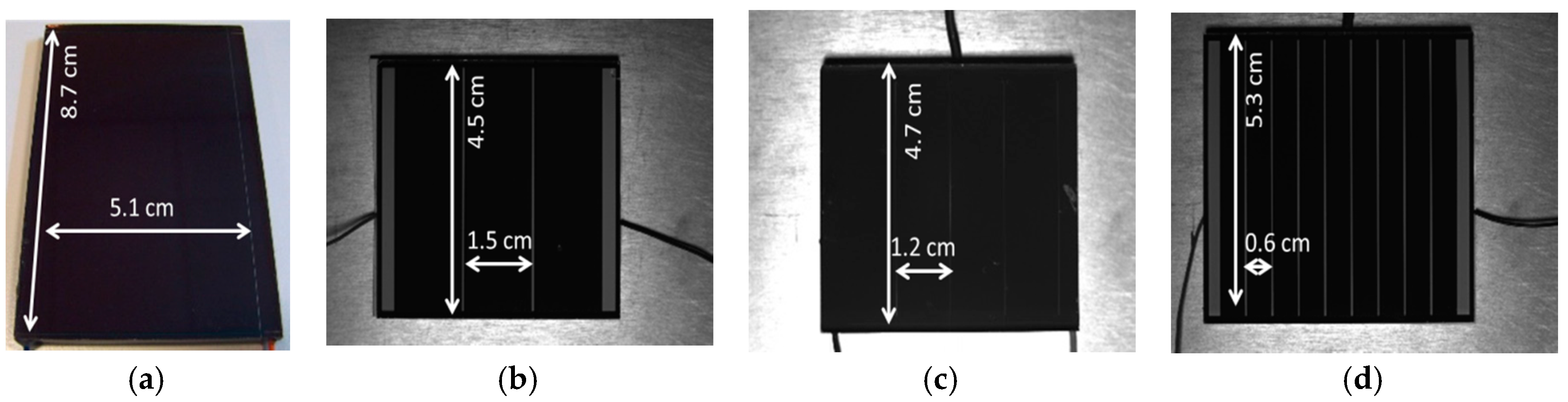
2.1. Samples

The experiment was conducted on three small-area modules of single-junction a-Si PV technology. Its structure consisted of TCO coated glass, p-i-n layers of a-Si solar cells with metal contact, and EVA/ polymeric sheet. These mini-modules were labeled as TF-1, TF-3, TF-4 and TF-9 according to number of monolithic series connected cells in a module, as shown in Figure 1. The module area of TF-1, TF-3, TF-4 and TF-9 was 50 cm2, 24 cm2, 28 cm2 and 33 cm2, respectively. These modules were pre-conditioned by light soaking before subjecting to I-V and imaging characterization techniques. Figure 2 shows the I-V characteristics of all the modules under STC condition. Table 1 summarizes the electrical parameters of these modules from their global I-V curves, which shows that the maximum output power of all the mini-modules was in close range (0.12–0.15 W) and the electrical parameters per unit cell were comparable. As an exception, TF-1 module showed much lower FF and efficiency than other modules.

2.2. Spatially-Resolved Characterization Techniques

For the characterization of TCO resistive losses and localized defects in a-Si PV modules, EL, LIT and LBIC techniques have been performed under distinct operating modes, which are known as current dependent EL imaging, dark and illuminated LIT, and limited-LBIC, respectively. The experimental details of these imaging techniques applied on module have been presented here.

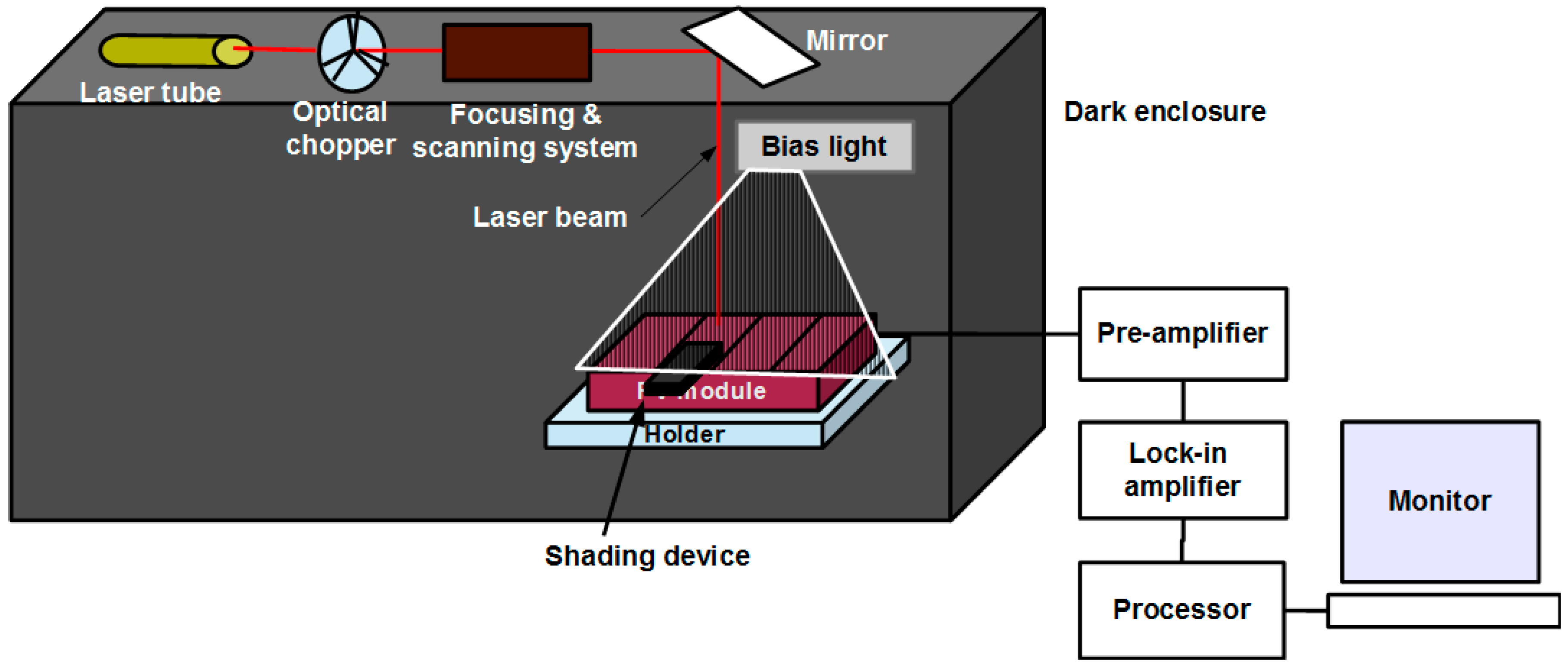
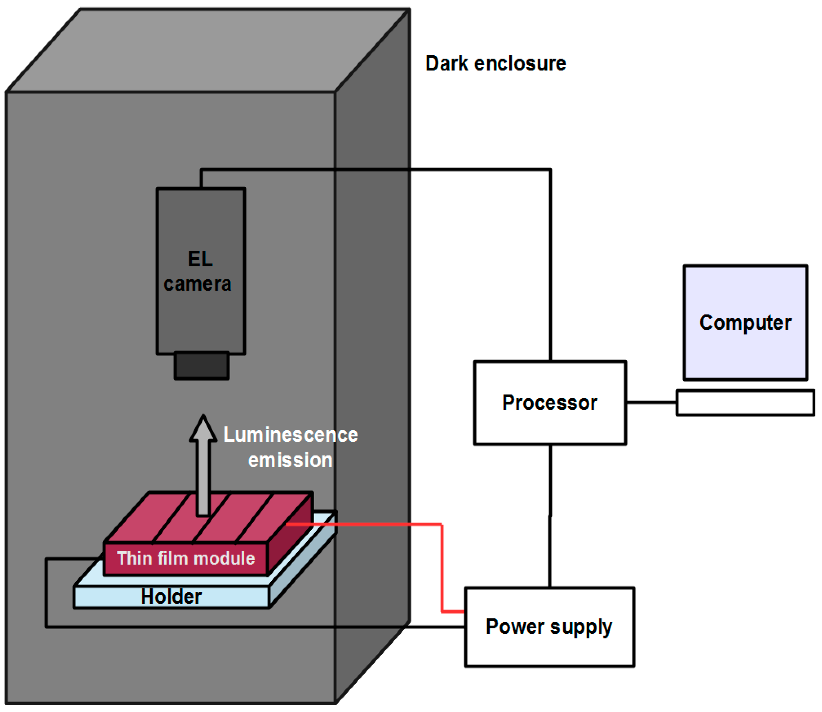
2.2.1. Current Dependent Electroluminescence Imaging

EL imaging is a fast characterization technique, which measures the luminescence emission via radiative recombination of minority carriers in the forward biased solar cell. It has been extensively used for spatial mapping of minority carrier diffusion length and series resistance, and detecting the cracks, finger defects in c-Si solar cells [36,37,38]. However, EL analysis of a-Si thin-film PV modules is not yet common due to the large density of band-tail states near the valence and conduction bands. In the presence of defect states, the radiative recombination decreases, whereas the non-radiative recombination increases, leading to weak luminescence emission [39,40]. In addition, a-Si exhibits low EL efficiency in the spectral range covered by the most commonly used Si-CCD detector. Furthermore, the distinction between several deficient areas in a grayscale EL image is very difficult since most of the defects appear dark. Some approaches have been employed on c-Si solar cells to differentiate between intrinsic and extrinsic defects, which utilized different cell temperature [41] or different spectral filters [42]. These approaches were also applied to a-Si solar module to find the artifacts and study the influence of temperature on spectral irradiance due to different types of radiative recombination [43]. The EL measurement at single current is intrinsically limited to distinguish the variety of defects present in the module. In this study, EL measurements were performed at two different current injection levels to obtain more useful information about the TCO sheet resistive losses as well as identification and classification of defects in the module.
The schematic of an experimental setup for EL imaging is given in Figure 3. It consists of a computer-controlled excitation source, an EL camera and a thin-film PV module. A power supply was used as an excitation source by injecting the current into the solar cells of module. An EL camera consisting of 1024 × 1024 pixels Si-CCD detector, was used to capture luminescence emission with the minimum spatial resolution of around 150 µm for the samples under investigation. Each pixel acquired an analog signal and transferred it to a computer in the form of a 16-bit image. EL camera was actively cooled to reduce the thermal noise and stabilize the spectral response of the detector. A computer was used for controlling the power supply and EL camera, and for storing the EL images. To distinguish different resistive losses in a module, EL measurements were performed at two current densities equivalent to module’s Jsc and one-tenth Jsc, representing high and low current injection conditions, respectively. The module was excited by passing the forward current, and the emitted luminescence from a-Si solar cells through the front glass was measured by the EL camera. In the case of a-Si modules, the acquisition time for each EL measurement under high and low current injection levels was kept at 3 min and 15 min, respectively, to obtain good signal-to-noise ratio. The longer integration time, in contrast to wafer-based c-Si modules is due to poor quality of a-Si material, which results in the weak luminescence emission. The experiment was performed in a complete dark enclosure to minimize the effects of unwanted stray light on the output results. Further, an image subtraction was employed on the EL images of module with and without excitation to eliminate bad pixels of the detector as well as to minimize the background noise, which improves the image quality. The resultant EL data were mapped into a grayscale image by the image processing software, for investigation of TCO lateral resistance effects and other localized defects in a-Si thin-film modules.

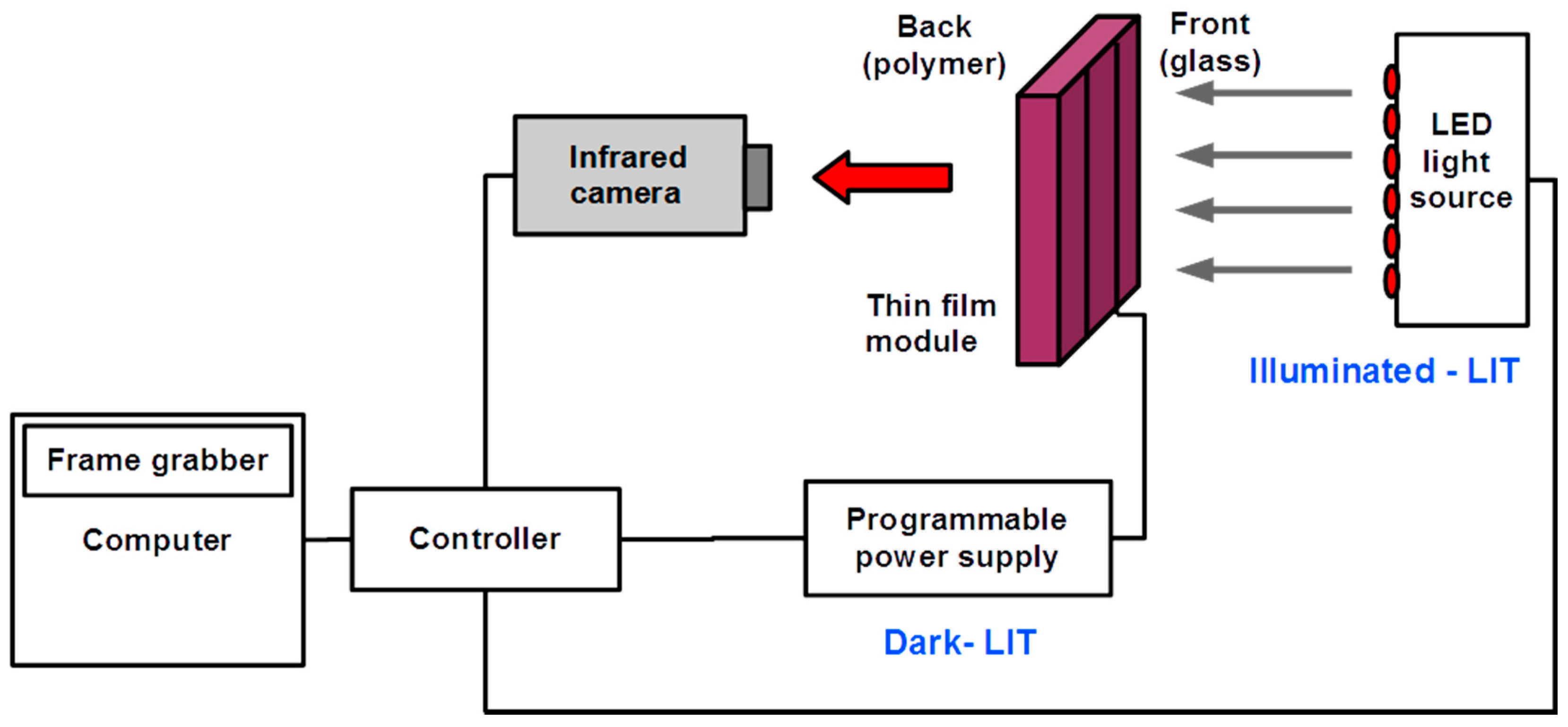
2.2.2. Dark and Illuminated Lock-In Thermography

LIT technique has been widely used for the detection and characterization of in-homogeneities that cause extra power dissipation in the solar cells [11]. It is based on the fundamental principle that the local anomalies affect the current flow through the contacts and give heat signatures in the thermal images. The inbuilt lock-in mode greatly reduces the noise of measurement, which improves the signal-to-noise ratio and spatial resolution as compared to traditional mode of thermography. It is a well-established technique for the single solar cells. However, this technique has not been reported much for module investigation since the experimentation and analysis of results for an encapsulated module are not as easy and straightforward as in the case of a single cell [44]. A PV module has a thick glass on the front side, which is almost opaque to infrared (IR) radiations, making it difficult to image the solar cells through the glass. The low thermal diffusivity of glass also considerably reduces the spatial resolution. A polymeric material was present at the backside of module, which is also opaque to IR radiations, but its thickness is less than that of the front glass. While considering these facts, the investigation on PV module was carried out from its backside. Still, some extent of signal degradation may be induced by the packaging materials above the cells, which lowers the spatial resolution as compared to a bare solar cell. LIT method is mainly used for the detection of processing induced defects or shunts in thin-film modules; however, it is less utilized for investigation of TCO resistance losses in thin-film PV modules. In the present study, LIT technique has been exploited to image the spatial distribution of series and shunt resistance losses in a-Si modules. The LIT measurements were performed under dark and illuminated conditions, which are known as dark lock-in thermography (DLIT) and illuminated lock-in thermography (ILIT), respectively. DLIT detects the flow of dark current through the device, which analyzes the resistive losses. While ILIT investigates the resistive losses in module under illumination at short-circuit (Jsc-ILIT) and open-circuit (Voc-ILIT) conditions. In such case, the module operates at two extreme regions on its I-V characteristic curve, where one particular resistance is more sensitive than the other, i.e., Rs losses are dominating at high voltage regimes while shunts are prominent at low voltages. On that basis, this method can allow to separate out different resistive losses in the module.
Figure 4 shows the schematic of the experimental setup for LIT under dark and illuminated conditions for the investigation of TCO resistive losses and shunts in thin-film modules. It comprises of an excitation source, an IR camera, a controller, a computer and a-Si thin-film PV module. LIT measurements were performed by a stirling-cooled IR camera of 320 × 256 pixels made of InSb detector with sensitivity in the spectral range of 3–5 µm, which measures the temperature modulation on the backside of module with a minimum spatial resolution of around 400 µm for the samples under investigation. The noise equivalent temperature difference (NETD) of the detector at 25 °C was less than 25 mK. Both DLIT and ILIT approaches utilized the same imaging system, but different excitation source. In DLIT, the module was excited by passing a periodic current from a programmable power supply under forward bias, whereas, in ILIT, a periodic illumination was provided over the front surface of module by red light (625 nm wavelength) LED array system consisting of 240 LEDs of 3 W each along with an integrated air-cooling mechanism. The illumination intensity over the module surface was 850 W/m2 with non-uniformity less than 5%. In Jsc-ILIT mode, the module terminals were shorted, while in Voc-ILIT, the contacts were left open. A controller was used to synchronize the power supply excitation with the frames of IR camera to implement lock-in algorithm over the captured images. The modulation (or lock-in) frequency, which is reciprocal of thermal diffusion length, was fixed at 0.5 Hz. The thermal images were acquired at a frame rate of 150 Hz for 200 s. Higher integration time is needed to improve signal-to-noise ratio of the captured images as it facilitates the averaging over a number of cycles that reduces the noise level. All the measurements were carried out at constant room temperature of 25 °C.

2.2.3. Limited-Light Beam Induced Current

LBIC is an optical scanning method which yields the spatial mapping of photocurrent generation over a solar cell under short-circuit condition in the dark surroundings. In the case of the module, when a solar cell is locally illuminated, the remaining cells get reverse biased and restrict the output photocurrent. The output LBIC signal is significantly affected by the electrical parameters (mainly shunt resistance) of other cells and could not represent the true local properties of the investigated cell [45]. Another approach of LBIC, i.e., illuminated-LBIC was used where an external bias illumination was provided over the entire module area. However, it is difficult to achieve large area uniform illumination with good accuracy that affects the LBIC signal strength and could give misleading information [46]. In order to overcome this limitation, the method has been modified where the active cell is brought into the limiting condition by means of partial shading. The shaded cell determines the module current and measures the true cell properties in the output. This approach is known as limited-LBIC (li-LBIC), which has been used for better assessment of spatial mapping of cell photo-generation current in a module in a non-destructive manner [45].
The schematic of the experimental setup for li-LBIC method is illustrated in Figure 5. It comprises of a laser, optical chopper, scanning and focusing system, lock-in amplifier, bias light, a thin-film PV module and a shading device. A helium-neon laser (633 nm wavelength) having a spot diameter of 0.41 mm was used for local illumination of solar cell in a module. The beam intensity affects the concentration of charge carriers that is related to the signal strength, while the beam diameter limits the spatial resolution of the image. A smaller beam diameter improves the spatial resolution; however, it will considerably increase the scan time. The laser beam was modulated using an optical chopper before passing through the focusing system and scanning head. The galvanic mirror directed the laser beam to fall on the PV module, placed on a two-axes translation stage. The laser beam illuminated a very small area of the solar cell, which was partially covered by a shading device of metal sheet with its width equal to that of the investigated cell. A uniform bias illumination was also provided over the entire module by an array of halogen lamps. The photocurrent on each point of module was collected under short-circuit condition and sent to a preamplifier which converts the signal to a voltage, which was then measured with a lock-in amplifier where the reference modulation frequency was taken from the optical chopper. In similar fashion, the laser beam was allowed to move and scan each point of the cell. The complete cell area was scanned by moving the shading device to the previously unshaded side of cell. The resultant image of module was made by stitching together two LBIC images of upper and lower portions of each cell, obtained after partial shading of the cell. The photocurrent map obtained from this method has been analyzed to see the impact of localized defects on the generation capabilities of cell, which in turn represents the cell performance in a module.

3. Results and Discussion

In this section, the experimental results of current dependent EL, dark and illuminated LIT, and limited-LBIC are given for imaging different parasitic resistive losses and related defects in a-Si thin-film modules. Results from these techniques have been compared and analyzed for a particular type of parasitic effect, with their relative advantages and limitations. In addition, more detailed analysis of these effects has been performed from the combined information of individual techniques.

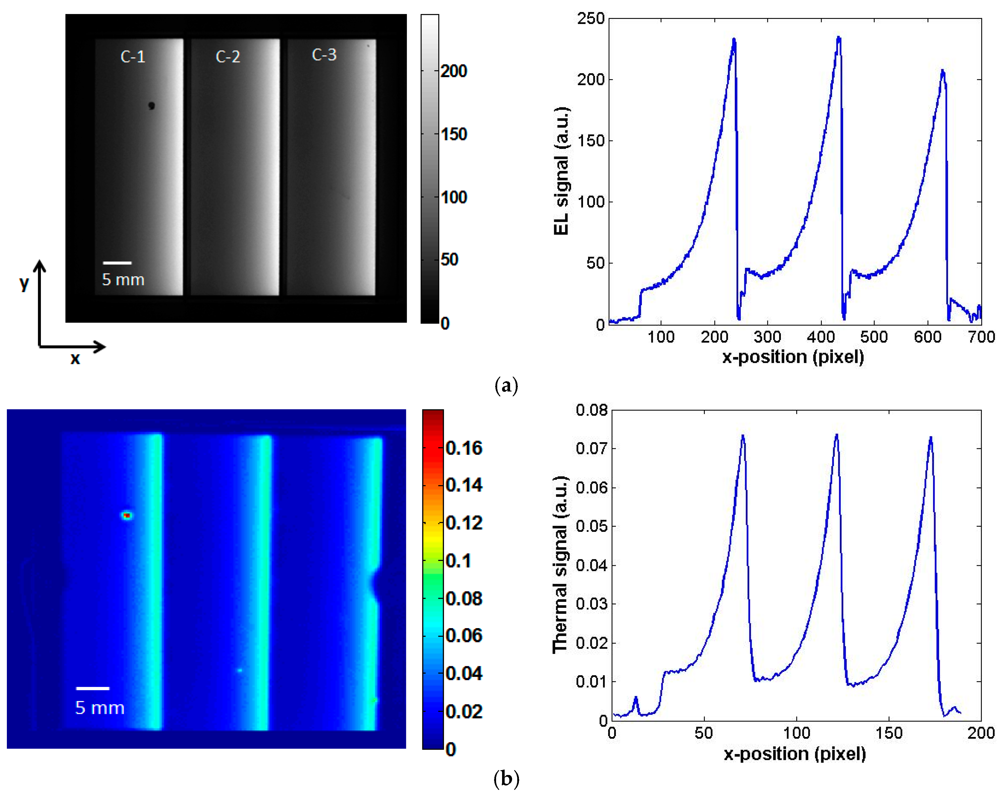
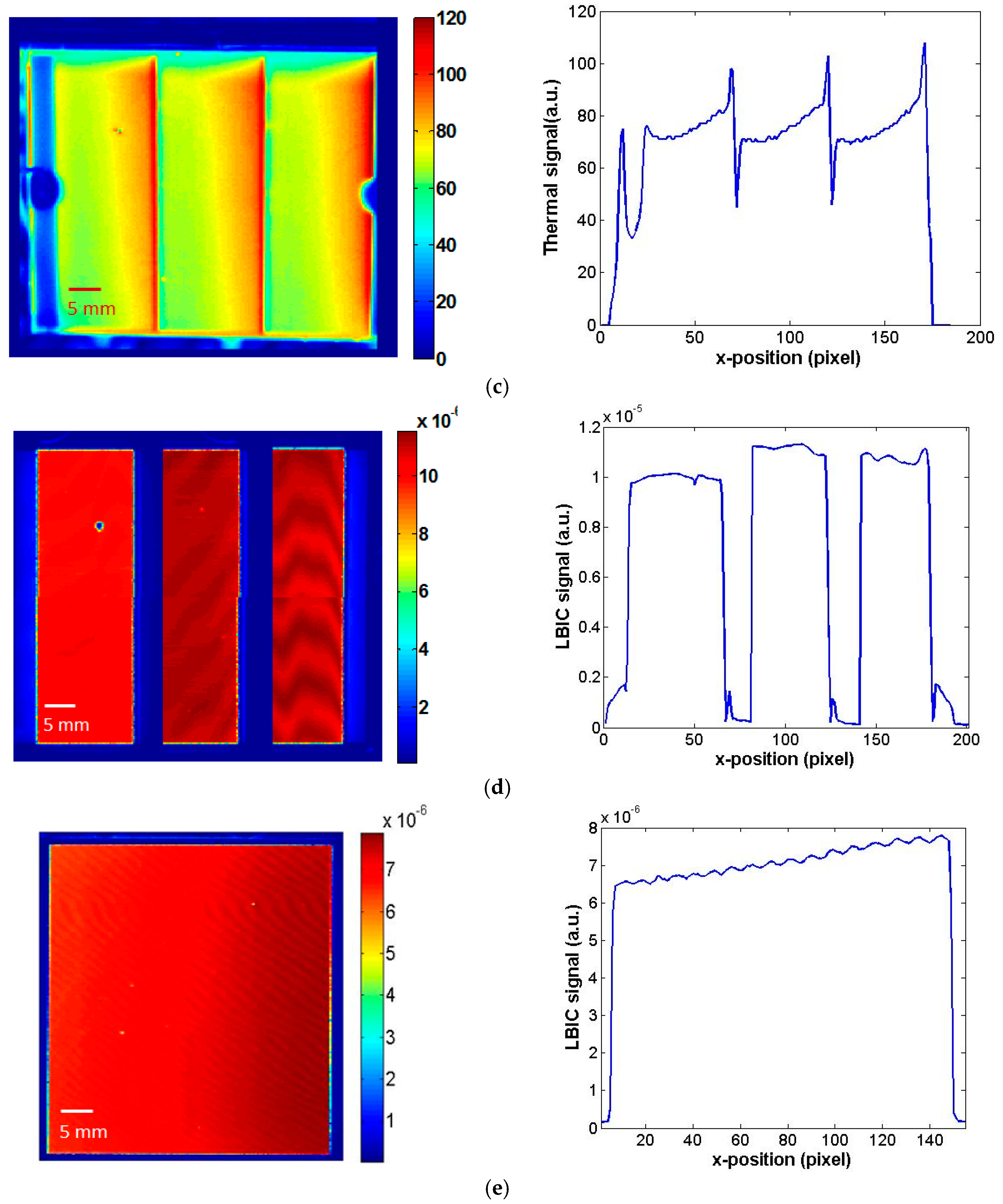
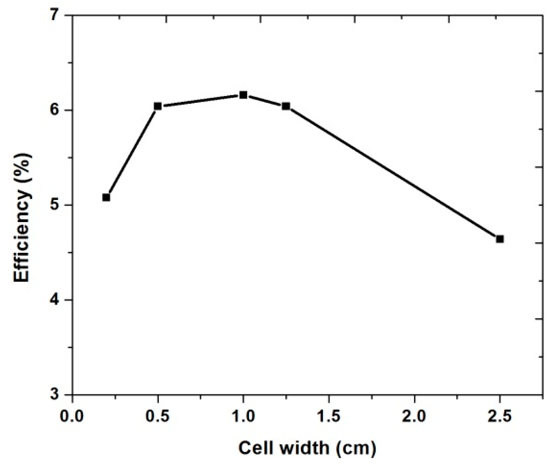
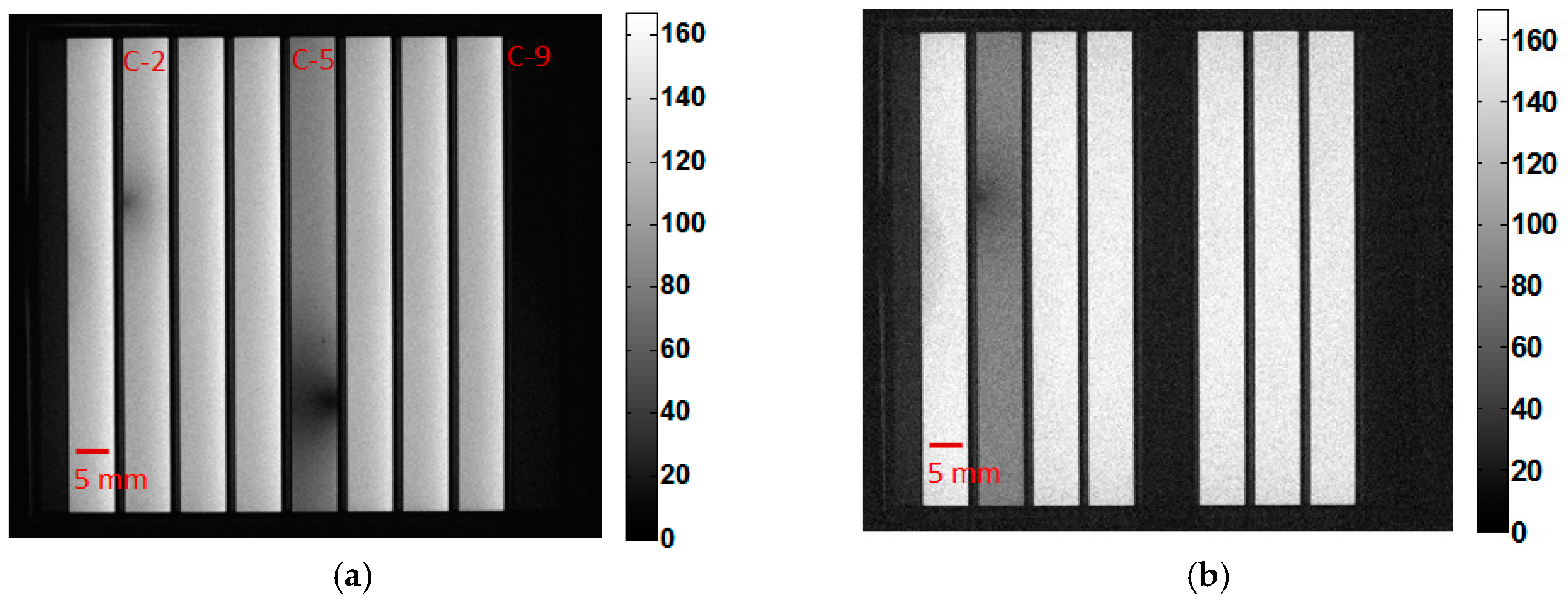
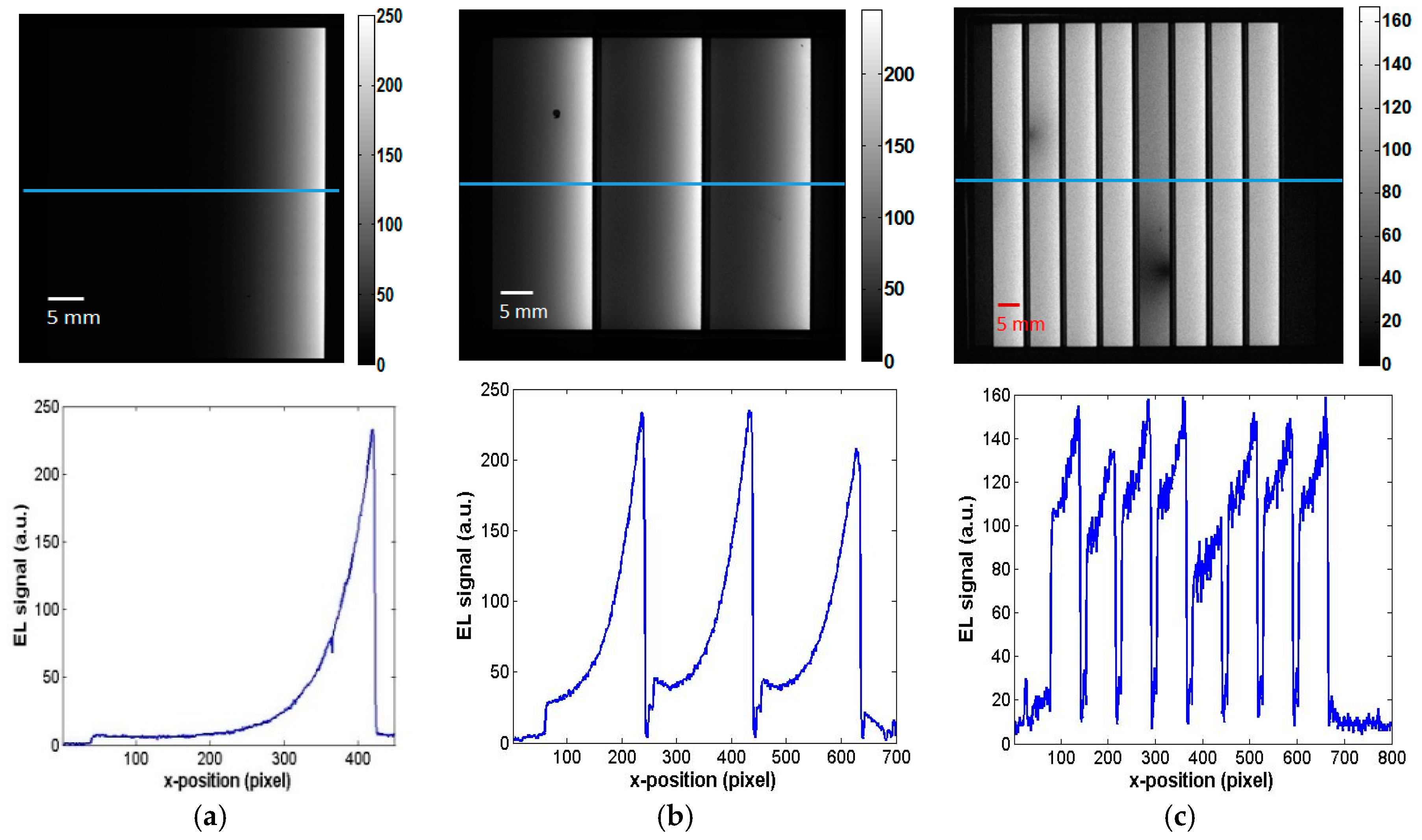
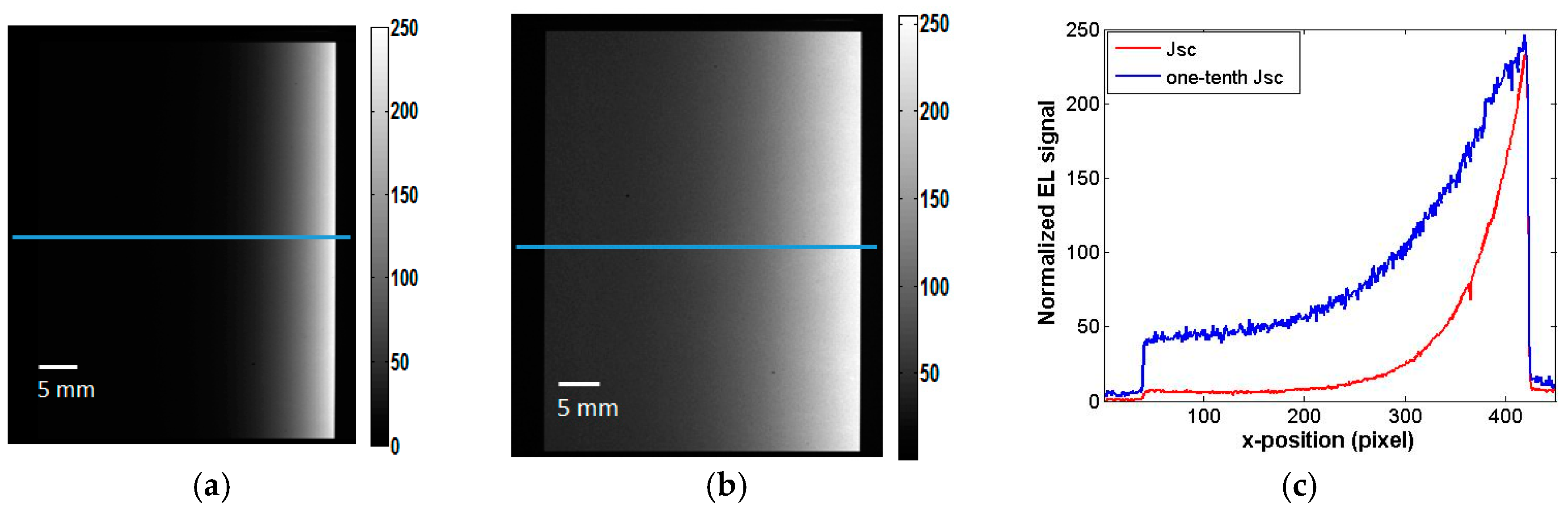
3.1. TCO Lateral Resistance Imaging
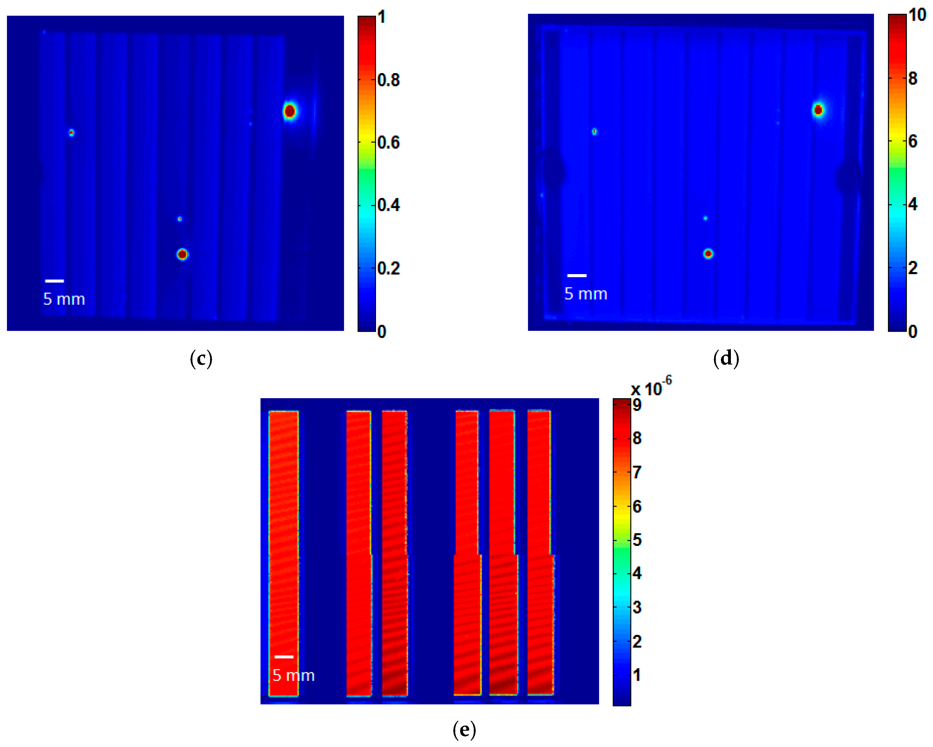
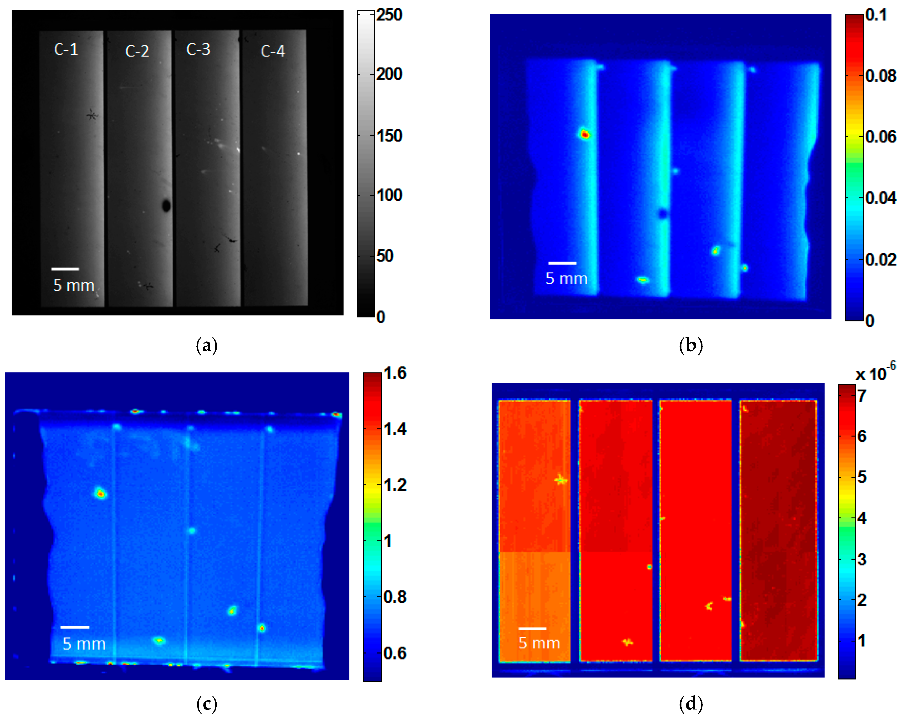
EL imaging has been used for the analysis of lateral sheet resistance of TCO layer in the modules, which significantly influence the module electrical performance. The relation between EL intensity and electrical parameter has been exploited for obtaining the information related to the lateral sheet resistance of TCO layer. Figure 6a presents the EL image and its line scan along the width of TF-3 sample at Jsc, which shows a characteristic gradient of EL emission along the width of a cell between the contacts (x-direction), whereas there was almost no change in EL intensity along the vertical direction (y-direction). This gradient is due to the lateral current flow along the cell width that causes voltage drop across lateral sheet resistance of TCO. The rate at which EL intensity reducing from its peak is related to sheet resistance of TCO layer and overall EL intensity drop across the cell is related to the cell resistance per unit length faced by the current flowing in lateral direction. For quantification of TCO sheet resistance, a current fitting iterative method has been adopted [24]. For this purpose, simulation based on the distributed diode model of thin-film PV module has been exploited using PSpice circuit simulator. In this simulation, a PV module has been divided into a specific number of sub-cells and the electrical parameters of each sub-cell has been estimated from the global I-V parameters of module. The electrical properties of all cells in the module have been assumed to be identical. The current distribution across the cell has been simulated by changing the sheet resistance in an iterative manner to match with the experimentally obtained results for the estimation of TCO sheet resistance. The estimated value of sheet resistance was around 14 Ω/□, which has been used later for further simulation.
In order to relate the sheet resistance effect with the localized heating in a module, DLIT and Jsc-ILIT techniques have been exploited. Figure 6b,c presents the DLIT and Jsc-ILIT images along with the line profiles of TF-3 sample, respectively. Both the images show a thermal gradient, which appears due to the variation of power dissipation along the cell width. In DLIT, the lateral flow of external current is high at injection edge and low at collection edge of the cells due to lateral sheet resistance effect of TCO layer, which decreases the power dissipation and corresponding thermal signal from the injection edge. Jsc-ILIT image also shows thermal gradient across the cell width. However, the spatial variation of thermal signal in ILIT exhibited a slower decline as compared to DLIT because almost uniform current is generated all across the cell in ILIT, whereas, in the case of DLIT, the current flowing across the cell is non-uniform. The small non-uniformity of thermal signal along y-direction in the image is due to slight non-homogeneous illumination at the module surface. ILIT appears to be less sensitive to the variation of sheet resistance compared to EL and DLIT near the higher potential edge, while in the case of larger width cells, it will be more sensitive near lower potential edge where output signals of DLIT and EL get almost saturated.
LBIC technique has also been used for TCO sheet resistance imaging. Figure 6e shows LBIC image of a single cell along with its line profile, which give a gradient pattern of signal along the cell width. The photo-generated current at different positions in the cell flows through different TCO resistance depending on the distance from the collection edge, creating this gradient pattern. To examine the response in the case of module, current limited LBIC technique has been applied to TF-3 sample, as shown in Figure 6e. In this case, the gradient pattern along the cell width due to TCO lateral sheet resistance is not visible in any cell of the module because resistance effect would be masked by other cells in series and partial shading of cell under investigation. It indicates the insensitivity of this technique for imaging TCO sheet resistance effect in a module compared to EL and LIT techniques.
The above results infer that both EL and LIT imaging techniques show the effects of TCO lateral sheet resistance in a module. In the case of LIT method, the magnitude and spatial resolution of thermal signal get affected by the encapsulant materials around the absorber layer and surrounding conditions, however EL signal is not affected by these factors. Therefore, EL signal is more reliable for quantitative analysis of TCO sheet resistance in the module. In addition, EL characterization is faster than LIT because the latter takes a longer time to reduce noise by averaging over several excitation cycles. Moreover, EL system uses relatively low cost CCD camera compared to cooled IR camera in LIT system.
It was observed that the gradient pattern due to the lateral sheet resistance of TCO layer is mainly influenced by two factors, first is the width of a solar cell and second is the current flowing in the cell. In order to relate the gradient pattern with cell width, EL imaging has been performed on the modules of different cell width at same short-circuit current density. Figure 7a–c shows the EL images of TF-1, TF-3 and TF-9 samples along with its line scan over a non-defect region of a module. The images show a decline in the EL intensity across the cell with the increase in cell width. It is more evident from the line scans that decrease in EL intensity was higher in TF-1 sample as compared to TF-3 sample, which in turn higher than TF-9 sample. It is due to the fact that a wider cell offers more TCO lateral resistance to the current flow in a cell, causing higher voltage drop. The drop in EL intensity is showing a pattern similar to the exponential decay in wider cells; however, for narrower cells, EL intensity pattern appears to be linear. The overall decrease in EL intensity across the cell signifies TCO resistive losses, which is higher for modules having a larger cell width. Thus, the width of a cell considerably affects the series resistance losses in a cell, which appears to be responsible for low FF and efficiency of TF-1 sample, as given in Table 1. This signifies that high TCO lateral resistance can cause significant power loss in a-Si or any other thin-film technology modules where TCO is used as the front electrode, especially the large-area solar cells. A smaller cell width will reduce the series resistive effect on individual cells and hence increase the overall efficiency of module; however, it will increase the total dead area (area between the cells), which would affect the module performance. Hence, the width of a cell is an important aspect to be considered while optimizing the design of module. For this purpose, the simulation based on the distributed diode model of thin-film module has been performed with varying cell width in a fixed module area. The area and electrical parameters of module under simulation were considered closer to TF-3 sample, including the measured TCO sheet resistance of 14 Ω/□. Figure 8 presents the variation of module efficiency with cell width. It shows that module efficiency increases with the decrease in cell width, which is attributed to the reduction in TCO resistive effect of individual cells, which would improve FF. However, a very small cell width will cause a significant increase in total dead area of the module that would reduce the efficiency after certain cell width.
Another factor affecting the intensity gradient is the magnitude of current flowing into the cell. To study the effect of current density on gradient pattern, EL imaging has been performed at two current injection levels on a same module. Figure 9a,b shows the EL images of TF-1 sample at Jsc and one-tenth Jsc, respectively. At high current level, there is a sharp decrease in EL intensity along the cell width from the injection edge, which is caused by higher voltage drop across the lateral resistances of TCO layer. On the contrary, the EL image at low current density showed lower spatial decrease in EL intensity due to reduced voltage drop. A line scan illustrating this effect is given in Figure 7c. It also shows that, at high current, the EL intensity gradient is more sensitive to sheet resistance near the injection edge and less sensitivity towards the collection edge as compared to the EL intensity gradient at lower current level. However, in the case of smaller cell width, these EL profiles will be truncated earlier and high current would give higher sensitivity across the entire cell width. Therefore, qualitative and quantitative investigation of lateral resistance of TCO layer would be more appropriate by high current EL imaging in the case of smaller cell width, which would show almost linear EL intensity pattern across the cell (as shown in Figure 7c).

3.2. Shunts Imaging

Shunt in a module sinks the current from its surrounding area that causes the reduction in module efficiency. These shunts have been investigated and compared by EL, LIT and LBIC imaging techniques, with their relative advantages and limitations. The combined information obtained from these techniques has also been utilized to get more insight about the nature and severity of shunts.
Shunts affect the local voltage in a cell, which has been investigated by EL imaging. Figure 10a displays the EL image of TF-9 sample consisting of nine cells, taken at Jsc. It shows some local reduction in EL intensity in the upper and lower portions of C-2 and C-5 cells respectively, whereas there was significant reduction of EL intensity in the entire C-9 cell. The local quenching of EL signal in two cells indicated the existence of shunts in the module (shunt #1 in C-2 and shunt #2 in C-5). Shunt draws the current from its surrounding area that causes the reduction in the local voltage and corresponding EL intensity. The region around the shunts appeared dark in EL image with a halo-shaped area of decreasing EL intensity along x-direction, which is an effect of lateral flow of current along the width of module. It is difficult to find the exact location of a shunt from these images. In addition, there are a variety of defects and other multiple reasons that inhibit the EL signal, making it difficult to confirm any reduction in EL intensity as a shunt. This problem has been elucidated by performing EL measurement at low current density (one-tenth Jsc) [47], whose image is given in Figure 10b. It shows a striking feature that the smeared region due to shunt gets extended over the entire cell. It is because at low current densities, the reduction in current through the shunts is much smaller as compared to the reduction in cell current; therefore shunt draws current from the larger surrounding region of cell, which reduces the potential and eventually the EL intensity of entire shunted cell reduces. The spread of reduction in EL intensity around a shunt depends on the shunt parameters, biasing conditions and positioning of a shunt in the cell. The severity of shunts can be estimated by the influencing area and reduced EL intensity with the varying biasing condition. Figure 10a,b shows that the shunt #2 in cell C-5 was more severe than shunt #1 in cell C-2. In this way, the current dependent EL imaging provides more insight into the identification and classification of shunts in terms of its severity as compared to EL imaging at a single current level. At higher current condition, the localization of such strong shunts improves in EL images; however, this method limits its precise localization in a module.
Shunts not only influence the voltage, but also cause extra heating in the device due to current sinking from the surrounding region. For imaging the shunts by its heating effect, LIT technique has been utilized which helps in localizing the heat generated by shunts and improving the signal-to-noise ratio. DLIT image of TF-9 sample is given in Figure 10c, which shows four distinct high temperature spots with sharp contours. Strongest shunt (shunt #3) in the image appears near the left scribe line of cell C-9, which causes a significant drop in cell voltage that leads to reduction of thermal and EL signal in entire cell. The other two shunts (shunt #1 and shunt #2) were also located near the scribe lines, but they are less strong as compared to shunt#3. While comparing the EL and LIT images, it is observed that strong shunts have better localization in LIT image as compared to EL image. Furthermore, DLIT identified an additional bright spot (shunt #4) in the middle of cell C-5, which was not clearly visible in EL image, considered as a weak shunt. It shows that DLIT is more sensitive than EL for the detection of shunts in a module. It is evident from line scan of EL intensity across the module (shown in Figure 7c) that strong shunts in the cells reduce the corresponding cell potential. The extent of brightness and area of shunts in DLIT image of module depends on the local shunt resistance and cell potential. As a consequence, the relative strength of shunts in module by DLIT is difficult to quantify without the knowledge of cell potential. Here, EL method can complement DLIT for the assessment of the relative severity of shunts by providing the additional information about the relative floating potential of individual cells from its peak EL intensity. The thermal images also revealed that most of the shunts are situated near the laser scribe lines, suggesting that these shunts might be caused by the improper laser patterning processes during the production. It is anticipated that the thermal impact due to an excessive laser dose from its pulse and scanner acceleration delay causes internal material modifications in a-Si absorber layer that resulted in the disruption of p-i-n junction, causing the formation of leakage current paths. While the shunts located away from scribe lines could be attributed due to the formation of pinholes or non-uniform deposition process, which rupture the junction and produce shunts. This information related to shunts helps the manufacturers in minimizing the shunts formation and preventing from the early degradation of modules, which would otherwise lead to significant performance loss. From I-V data (Table 1), it is observed that this module (TF-9) has the lowest Voc per unit cell and comparatively lower FF and efficiency, which can be attributed to the presence of strong shunts in this module. All four localized shunts in TF-9 sample also appear in the Voc-ILIT image in Figure 10d, though the thermal signal is different from DLIT image due to localized photocurrent generation. Under open-circuit condition, there is no external current path, therefore generated current flows towards the shunt position, causing the extra heating at shunt location. Voc-ILIT method, which is non-contact in nature, shows good agreement with DLIT method for shunt investigation in the thin-film modules. However, the comparison of ILIT images acquired at open-circuit and short-circuit conditions allows the distinction between the local shunting and TCO lateral sheet resistance effects in PV modules. There is also a shunt in TF-3 module at cell C-1 (Figure 6), which is clear from higher thermal signal in DLIT and lower luminescence signal in EL imaging. This defect was feebly visible in Jsc-ILIT image compared to DLIT image because in Jsc-ILIT, background heating due to uniform photo-generated current causes lower thermal contrast at shunt position, which makes the shunt effect more visible in DLIT.
The li-LBIC method has been exploited on this module to obtain the photocurrent response of strongly shunted cells. Figure 10e displays the li-LBIC image of the same module, where three cells (C-2, C-5 and C-9) of the module corresponding to the shunted cells produced very low signal in the entire cell. Strong shunt created a highly conductive path in the cell through which the photo-generated current sinks that caused low LBIC signal in entire shunt affected cells. This shows that LBIC method was unable to produce sufficient signal in these strong shunt affected cells. However, for weak shunt as seen in TF-3 sample, the present system could produce sufficient LBIC signal for detection of shunt position in the cell, as seen in Figure 6d. For detection of strong shunts, LBIC measurement at very high incident light flux could be useful.
From the comparison of results obtained with different characterization methods, it is inferred that EL, LIT and li-LBIC techniques can identify the shunted cells in a module. Results show that LIT technique allows best detection of all types of shunts, while EL provides insight into the severity of strong shunts due to the relative change in cell potential. LIT also provides valuable information about the possible root causes of shunt formation that will be useful in taking the appropriate corrective measures at each processing step to avoid severe degradation and performance loss of PV modules. Being a non-contact method, Voc-ILIT can be deployed for the inline detection of shunts in solar modules before making contacts. Further, LIT measurements can be performed in an open environment since the results are not significantly affected by the stray lights due to inbuilt lock-in feature. However, it has certain drawbacks, such as it needs an expensive IR camera and takes longer integration time. In comparison, the low cost EL method can be used for the identification and estimation of severity of shunts, but it requires a measurement at low current bias condition for confirmation of shunts. Low current EL measurement also requires longer integration time. Besides that it requires a dark environment for the measurement.

3.3. Scratches Imaging

Scratches are the surface defects that affect the module performance, which has been investigated by LIT, EL and LBIC imaging techniques. Figure 11a presents the EL image of TF-4 sample at Jsc, which shows some microscopic defects as dark spots (or cross-hair line structures) of different sizes, where the biggest spot was observed near the right scribe line of cell C-2. Lack of carrier concentration at defect regions reduces the EL intensity. The scratches show similar influence on the carrier density as of shunts. However, it is difficult to distinguish these defects from the shunts and other artifacts, which also reduce EL intensity.
In order to ascertain that these defects have shunting effect, LIT imaging has been performed. Figure 11b,c presents the DLIT and Voc-ILIT images of TF-4 sample, respectively. The edges of these images did not appear very smooth due to the presence of an adhesive layer near the edges, which affect thermal signal. Both the images show higher thermal signal at defect locations as compared to the background, which confirms that these scratches are also forming shunts. However, in DLIT images, the thermal signal at these shunts was lower compared to TF-9 sample, which indicates that these scratch-induced shunts are weak in nature. The localization of these weak shunts was better in DLIT image as compared to Voc-ILIT image, because in the case of Voc-ILIT, the background heating due to uniform photo-generated current in the cell affects the visibility of weak shunts. The comparison of these images with EL image shows that localization of these scratches was better in EL image because these weak shunts are not significantly affecting the surrounding region voltage. However, in the case of LIT, there was some blurring around the shunt due to thermal diffusion of heat, which can be improved to some extent by increasing the lock-in frequency, but higher lock-in frequency leads to lower signal that makes it difficult to detect weak shunts.
In order to examine the photo-response behavior of these defects, li-LBIC measurement has been performed. Figure 11d presents li-LBIC image of the same sample, which shows all the localized defects due to scratches with reduced photocurrent. The reduction in photo-generated current is in agreement with LIT result, which indicates these are shunts that sink the current and reduce the LBIC signal. Here, shunts are visible in li-LBIC image because these are weak shunt compared to shunts in TF-9 sample, where li-LBIC signal could not able to locate shunt position. As an exception, the localized reduction of LBIC signal at the defect near the right scribe line of C-2 cell of TF-4 sample, did not indicate a shunting effect according to LIT results. These weak shunts caused each cell to exhibit different photocurrent response depending upon the affected area by the scratches, which would influence the overall performance of module. The biggest region affected by scratch was present in the first cell (C-1) that lowers the LBIC signal of entire cell as compared to other cells in the module. In other cells, the electrical damage caused by other scratches was lower in terms of photocurrent generation, which is evident by the color contrasts. Thus, li-LBIC method enables the assessment of photocurrent loss due to defects and evaluates the relative current generation performance of individual cells in a module, which is not coming from EL and LIT techniques. This module exhibited higher FF than TF-9 sample, indicating these defects lead to relatively lower shunting that do not considerably deteriorate the module performance.
As discussed earlier, defect at the right scribe line of C-2 cell was showing lower signal in DLIT image (Figure 11b), which indicates that this defect is not a shunt, but could be high recombination active region as appearing from the low EL signal (Figure 11a). However, this region is not distinguishable in Voc-ILIT image (Figure 11c) because heat generated all across the cell overshadows this small defected region. The li-LBIC image (Figure 11d), which is more sensitive to image photo-generation with good localization, is showing this region with reduced photocurrent ascertained that this region is of poor diode quality or high recombination active region having good shunt resistance. This type of defect is common in modules, which is difficult to understand by a single imaging technique. Hence, the cross-characterization also helped in identifying such defect with possible impact and origin.
The above characterization results show that LIT is useful in the identification of scratches that lead to shunts in the cells, while EL provides better localization of such weak shunts. On the other hand, li-LBIC method appears to be a reliable diagnostic tool for investigating the relative impact of such weak shunts on the photocurrent generation capability of each cell in a module.
The present study was performed on a-Si thin-film PV module technology; however, it can also be applied to other thin-film module technologies, since TCO is generally used as a front contact in thin film technologies and modules are fabricated in a similar manner via monolithic integration of individual cells. Further, the investigated resistive losses generally exist in other thin-film technology modules, which deteriorate the performance and reliability of PV modules.

4. Conclusions

In this paper, imaging of parasitic resistive effect due to TCO lateral resistance, shunts and scratches in thin film module has been investigated by a combination of current dependent EL, dark and illuminated LIT, and limited-LBIC techniques. Results obtained from individual techniques have been compared and analyzed with their relative advantages and limitations for a particular type of resistive loss channel based on its severity. EL, DLIT and Jsc-ILIT techniques showed TCO lateral resistance effect in the module. EL and DLIT found to be more sensitive to TCO sheet resistance compared to Jsc-ILIT near the higher potential edge of cell, while, in the case of wider cell, Jsc-ILIT was more sensitive near lower potential edge. It indicates that for narrower cells, EL and DLIT lead to higher sensitivity across the entire cell width. EL method was advantageous compared to LIT for the quantitative analysis of sheet resistance, which has been calculated and used in relating cell width with module efficiency in a particular module by simulation based on distributed diode model. DLIT technique comes out to be better than EL and LBIC techniques for the detection of shunts of different severity; however, EL can complement DLIT for assessment of the relative severity of shunts by providing additional information about the relative floating potential of individual cells. LIT showed good localization of strong shunts in a module, while EL showed good localization for weak shunts which could arise from scratches. ILIT technique under short-circuit and open-circuit conditions enabled separating out the shunting and TCO sheet resistance effects. Where, li-LBIC method was not able to show the TCO lateral resistive effects and strong shunts in a module, however it was able to detect weak shunt with good localization and their impact on the photocurrent generation of individual cells. The combined information obtained from EL, DLIT and LBIC techniques have identified a localized region of high recombination in module, which was difficult to ascertain by a single technique. Results also show that cross-characterization by different imaging techniques helps in identification, classification, and quantification of different loss channels, as well as the appropriateness of each technique for investigating the particular loss or defect in PV modules. The present investigation can also be performed on other thin-film module technologies, since they also suffer from similar losses and defects.

Acknowledgments

This work has been supported by a joint India–UK initiative in solar energy through a joint project “Stability and Performance of Photovoltaics” (STAPP) funded by Department of Science and Technology (DST) in India and Research Councils UK (RCUK) Energy Programme in UK (Contract No. EP/H040331/1).

Author Contributions

Archana Sinha, Rajesh Gupta and Ralph Gottschalg conceived and designed the experiments; Archana Sinha, Martin Bliss and Xiaofeng Wu performed the experiments; Archana Sinha, Martin Bliss, Subinoy Roy and Rajesh Gupta analyzed the data; Xiaofeng Wu and Ralph Gottschalg ordered the experimental samples; and Archana Sinha and Subinoy Roy wrote the paper.

Conflicts of Interest

The authors declare no conflict of interest.

Abbreviations

The following abbreviations are used in this manuscript:
PVPhotovoltaic
TCOTransparent Conductive Oxide
ELElectroluminescence
LITLock-in thermography
LBICLight beam induced current

References

  1. Brecl, K.; Topič, M.; Smole, F. A detailed study of monolithic contacts and electrical losses in a large-area thin-film module. Prog. Photovolt. Res. Appl. 2005, 13, 297–310. [Google Scholar] [CrossRef]
  2. Lee, S.S.; Kim, Y.N.; Shin, H.G. Thermal Degradation Behavior of Aluminum-Doped Zinc-Oxide Thin Films Prepared by Using a Sol-Gel Process. J. Korean Phys. Soc. 2008, 53, 188–191. [Google Scholar]
  3. Lemire, H.M.; Peterson, K.A.; Sprawls, S.; Singer, K.; Martin, I.T.; French, R.H. Degradation of transparent conductive oxides: Mechanistic insights across configurations and exposures. In Proceedings of the SPIE 8825, Reliability of Photovoltaic Cells, Modules, Components and Systems VI, San Diego, CA, USA, 25 August 2013.
  4. Mirletz, H.M.; Peterson, K.A.; Martin, I.T.; French, R.H. Degradation of transparent conductive oxides: Interfacial engineering and mechanistic insights. Sol. Energy Mater. Sol. Cells 2015, 143, 529–538. [Google Scholar] [CrossRef]
  5. Dongaonkar, S.; Servaites, J.D.; Ford, G.M. Universality of non-ohmic shunt leakage in thin-film solar cells. J. Appl. Phys. 2010, 108, 124509. [Google Scholar] [CrossRef]
  6. Fortes, M.; Comesaña, E.; Rodriguez, J.A.; Otero, P.; Garcia-Loureiro, A.J. Impact of series and shunt resistances in amorphous silicon thin film solar cells. Sol. Energy 2014, 100, 114–123. [Google Scholar] [CrossRef]
  7. Lapinski, M.; Domaradzki, J.; Prociow, E.L.; Sieradzka, K.; Gornicka, B. Electrical and optical characterization of ITO thin films. In International Students and Young Scientists Workshop “Photonics and Microsystems”; IEEE: Wernigerode, Germany, 2009; pp. 52–55. [Google Scholar]
  8. Szitasi, G.; Korsos, F.; Selmeczi, D. Integrated Electrical and Optical Characterization of Large Area Thin Film Photovoltaic Materials. In Proceedings of the 38th IEEE Photovoltaic Specialists Conference, Austin, TX, USA, 3–8 June 2012; pp. 474–478.
  9. Fuyuki, T.; Kondo, H.; Yamazaki, T.; Takahashi, Y.; Uraoka, Y. Photographic surveying of minority carrier diffusion length in polycrystalline silicon solar cells by electroluminescence. Appl. Phys. Lett. 2005, 86, 262108. [Google Scholar] [CrossRef]
  10. Fuyuki, T.; Kondo, H.; Kaji, Y.; Ogane, A.; Takahashi, Y. Analytic findings in the electroluminescence characterization of crystalline silicon solar cells. J. Appl. Phys. 2007, 10, 023711. [Google Scholar] [CrossRef]
  11. Breitenstein, O.; Rakotoniaina, J.P.; Al Rifai, M.H. Quantitative Evaluation of Shunts in Solar Cells by Lock-in Thermography. Prog. Photovolt. Res. Appl. 2003, 11, 515–526. [Google Scholar] [CrossRef]
  12. Breitenstein, O.; Gupta, R.; Schneider, J. Surface potential mapping on crystalline silicon on glass solar modules. J. Appl. Phys. 2007, 102, 024511. [Google Scholar] [CrossRef]
  13. Filipič, M.; Holman, Z.C.; Smole, F.; De Wolf, S.; Ballif, C.; Topič, M. Analysis of lateral transport through the inversion layer in amorphous silicon/crystalline silicon heterojunction solar cells. J. Appl. Phys. 2013, 114, 074504. [Google Scholar] [CrossRef]
  14. Fecher, F.W.; Adams, J.; Vetter, A.; Buerhop-Lutz, C.; Brabec, C.J. Loss analysis on CIGS-modules by using contactless, imaging illuminated lock-in thermography and 2D electrical simulations. In Proceedings of the 40th IEEE Photovoltaic Specialist Conference, Denver, CO, USA, 8–13 June 2014; pp. 3331–3334.
  15. Bachmann, J.; Buerhop-Lutz, C.; Steim, R. Highly sensitive non-contact shunt detection of organic photovoltaic modules. Sol. Energy Mater. Sol. Cells 2012, 101, 176–179. [Google Scholar] [CrossRef]
  16. Seeland, M.; Rösch, R.; Muhsin, B.; Gobsch, G.; Hoppe, H. Electroluminescence as characterization tool for polymer solar cells and modules. Energy Procedia 2011, 31, 167–172. [Google Scholar] [CrossRef]
  17. Rösch, R.; Krebs, F.C.; Tanenbaum, D.M.; Hoppe, H. Quality control of roll-to-roll processed polymer solar modules by complementary imaging methods. Sol. Energy Mater. Sol. Cells 2012, 97, 176–180. [Google Scholar] [CrossRef]
  18. Runai, F.R.; Schwäble, F.; Walter, T. Imaging and performance of CIGS thin film modules. In Proceedings of the 37th IEEE Photovoltaic Specialist Conference, Seattle, WA, USA, 19–24 June 2011; pp. 3399–3403.
  19. Zaunbrecher, K.; Johnston, S.; Sites, J.R. Analysis of thin-film inhomogeneities using electroluminescence and LBIC measurements. In Proceedings of the 39th IEEE Photovoltaic Specialists Conference, Tampa, FL, USA, 16–21 June 2013; pp. 166–169.
  20. Feron, K.; Nagle, T.J.; Rozanski, L.J.; Gong, B.B.; Fell, C.J. Spatially resolved photocurrent measurements of organic solar cells: Tracking water ingress at edges and pinholes. Sol. Energy Mater. Sol. Cells 2013, 109, 169–177. [Google Scholar] [CrossRef]
  21. Besold, S.; Hoyer, U.; Bachmann, J.; Swonke, T.; Schilinsky, P.; Steim, R.; Brabec, C.J. Quantitative imaging of shunts in organic photovoltaic modules using lock-in thermography. Sol. Energy Mater. Sol. Cells 2014, 124, 133–137. [Google Scholar] [CrossRef]
  22. Bliss, M.; Wu, X.; Bedrich, K.G.; Bowers, J.W.; Betts, T.R.; Gottschalg, R. Spatially and spectrally resolved electroluminescence measurement system for photovoltaic characterisation. IET Renew. Power Gener. 2015, 9, 446–452. [Google Scholar] [CrossRef] [Green Version]
  23. Helbig, A.; Kirchartz, T.; Schaeffler, R.; Werner, J.H.; Rau, U.H. Quantitative electroluminescence analysis of resistive losses in Cu(In,Ga)Se2 thin-film modules. Sol. Energy Mater. Sol. Cells 2010, 94, 979–984. [Google Scholar] [CrossRef]
  24. Seeland, M.; Rösch, R.; Hoppe, H. Quantitative analysis of electroluminescence images from polymer solar cells. J. Appl. Phys. 2012, 111, 024505. [Google Scholar] [CrossRef]
  25. Wu, X.; Bliss, M.; Sinha, A.; Betts, T.; Gupta, R.; Gottschalg, R. Distributed electrical network modelling approach for spatially resolved characterisation of photovoltaic modules. IET Renew. Power Gener. 2014, 8, 459–466. [Google Scholar] [CrossRef] [Green Version]
  26. Courtois, G.; Fuyuki, T.; Tani, A.; Salomon, A.; Cabarrocas, P.R. Quantitative assessment of TCO sheet resistance in thin-film silicon devices from electroluminescence images. In Proceedings of the 28th European Photovoltaic Solar Energy Conference and Exhibition, Paris, France, 30 September–4 October 2013; pp. 2484–2488.
  27. Paire, M.; Lombez, L.; Guillemoles, J.F.; Lincot, D. Measuring sheet resistance of CIGS solar cell's window layer by spatially resolved electroluminescence imaging. Thin Solid Films 2011, 519, 7493–7496. [Google Scholar] [CrossRef]
  28. Shvydka, D.; Rakotoniaina, J.P.; Breitenstein, O. Lock-in thermography and nonuniformity modeling of thin-film CdTe solar cells. Appl. Phys. Lett. 2004, 84, 729–731. [Google Scholar] [CrossRef]
  29. Breitenstein, O.; Langenkamp, M.; Lang, O.; Schirrmacher, A. Shunts due to laser scribing of solar cells evaluated by highly sensitive lock-in thermography. Sol. Energy Mater. Sol. Cells 2001, 65, 55–62. [Google Scholar] [CrossRef]
  30. Zhang, L.; Xu, X.; Yang, Z.; Sun, X.; Xu, H.; Liu, H.; Shen, H. An efficient method for monitoring the shunts in silicon solar cells during fabrication processes with infrared imaging. J. Semicond. 2009, 30, 1–4. [Google Scholar]
  31. Chung, T.; Wang, C.H.; Chang, K.J.; Chen, S.Y.; Hsieh, H.H.; Huang, C.P.; Cheng, C.H.A. Evaluation of the spatial distribution of series and shunt resistance of a solar cell using dark lock-in thermography. J. Appl. Phys. 2014, 115, 034901. [Google Scholar] [CrossRef]
  32. Kasemann, M.; Schubert, M.C.; The, M.; Köber, M.; Hermle, M.; Warta, W. Comparison of luminescence imaging and illuminated lock-in thermography on silicon solar cells. Appl. Phys. Lett. 2006, 89, 224102. [Google Scholar] [CrossRef]
  33. Colvin, J. Comparative Failure Analysis of Photovoltaic Devices. In Proceedings of the 35th International Symposium for Testing and Failure Analysis, San Jose, CA, USA, 14–19 November 2009; pp. 149–156.
  34. Wehrmann, A.; Puttnins, S.; Hartmann, L.; Ehrhardt, M.; Lorenz, P.; Zimmer, K. Analysis of laser scribes at CIGS thin-film solar cells by localized electrical and optical measurements. Opt. Laser Technol. 2012, 44, 1753–1757. [Google Scholar] [CrossRef]
  35. Brooks, W.S.M.; Irvine, S.J.C.; Barrioz, V.; Clayton, A.J. Laser beam induced current measurements of Cd1−xZnxS/CdTe solar cells. Sol. Energy Mater. Sol. Cells 2012, 101, 26–31. [Google Scholar] [CrossRef]
  36. Würfel, P.; Trupke, T.; Puzzer, T.; Schäffer, E.; Warta, W.; Glunz, S.W. Diffusion lengths of silicon solar cells from luminescence images. J. Appl. Phys. 2007, 101, 123110. [Google Scholar] [CrossRef]
  37. Hinken, D.; Ramspeck, K.; Bothe, K.; Fischer, B.; Brendel, R. Series resistance imaging of solar cells by voltage dependent electroluminescence. Appl. Phys. Lett. 2007, 91, 182104. [Google Scholar] [CrossRef]
  38. Kajari-Schröder, S.; Kunze, I.; Köntges, M. Criticality of cracks in PV modules. Energy Procedia 2012, 27, 658–663. [Google Scholar] [CrossRef]
  39. Pankove, J.I. Radiative Recombination in Hydrogenated Amorphous Silicon. Czechoslov. J. Phys. B 1980, 30, 355–364. [Google Scholar] [CrossRef]
  40. Wang, K.; Han, D.; Silver, M.; Branz, H.M. Electroluminescence studies of recombination in hydrogenated amorphous silicon p-i-n devices. Sol. Energy 1991, 30, 219–225. [Google Scholar] [CrossRef]
  41. Fuyuki, T.; Kitiyanan, A. Photographic diagnosis of crystalline silicon solar cells utilizing electroluminescence. Appl. Phys. A Mater. Sci. Process. 2009, 96, 189–196. [Google Scholar] [CrossRef]
  42. Fuyuki, T.; Tani, A.; Tsujii, S.; Sugimura, E. Photographic distinction of defects in polycrystalline Si by spectroscopic electroluminescence. In Proceedings of the 35th IEEE Photovoltaic Specialists Conference, Honolulu, HI, USA, 20–25 June 2010; pp. 1380–1382.
  43. Predatsch, H.; Heinzmann, U.; Stiebig, H. Thin-film silicon solar cell and module analysis by electroluminescence. Energy Procedia 2014, 60, 71–75. [Google Scholar] [CrossRef]
  44. Breitenstein, O.; Warta, W.; Langenkamp, M. Lock-in Thermography—Basics and Use for Evaluating Electronic Devices and Materials, 2nd ed.; Springer: Heidelberg, Germany, 2010; pp. 213–214. [Google Scholar]
  45. Vorasayan, P.; Betts, T.R.; Gottschalg, R. Spatially distributed model for the analysis of laser beam induced current (LBIC) measurements of thin film silicon solar modules. Sol. Energy Mater. Sol. Cells 2011, 95, 111–114. [Google Scholar] [CrossRef]
  46. Roschier, S.; Agostinelli, G.; Dunlop, E.D. Laser scanning of amorphous silicon photovoltaic modules with different bias conditions. Opto-Electron. Rev. 2000, 8, 328–332. [Google Scholar]
  47. Gerber, A.; Huhn, V.; Tran, T.M.H. Advanced large area characterization of thin- film solar modules by electroluminescence and thermography imaging techniques. Sol. Energy Mater. Sol. Cells 2015, 135, 35–42. [Google Scholar] [CrossRef]
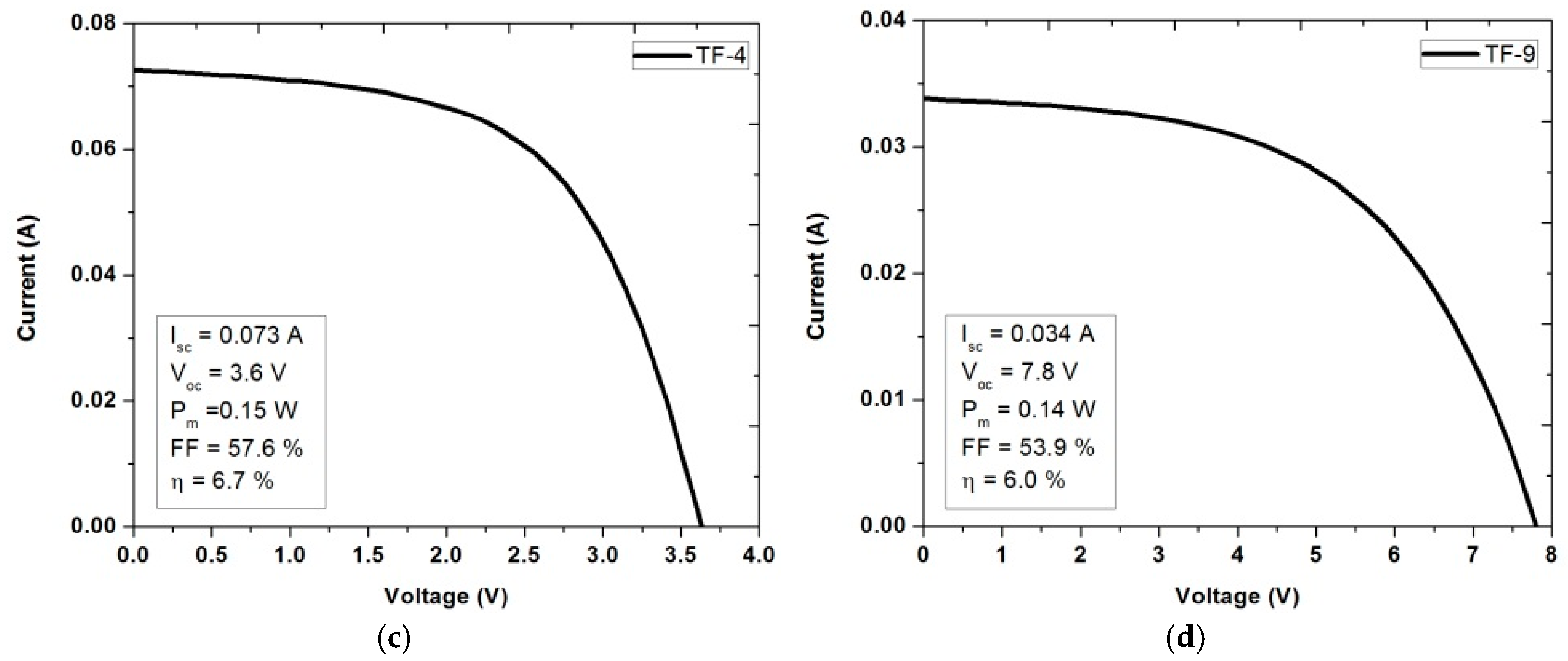
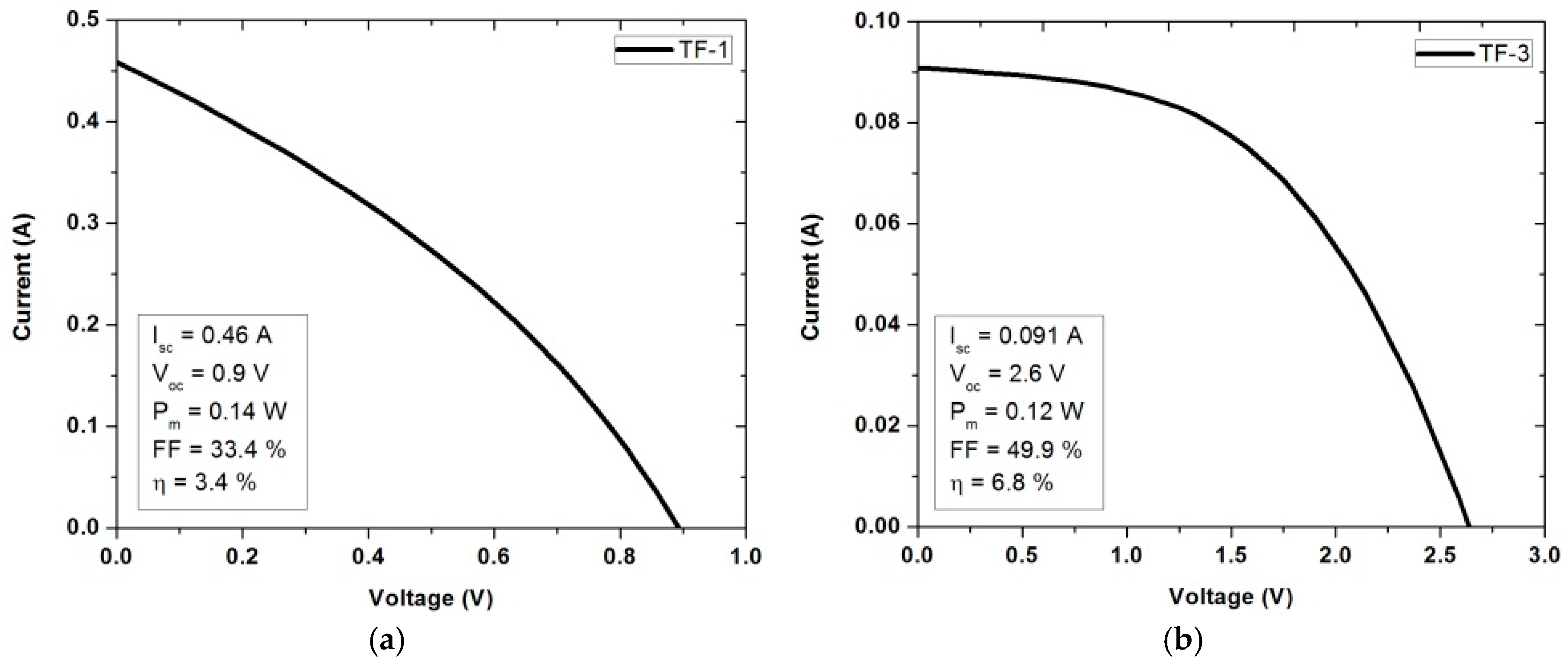
Figure 1. Visual images of a-Si mini-modules: (a) TF-1; (b) TF-3; (c) TF-4; and (d) TF-9.
Jimaging 02 00023 g001
Figure 2. I-V characteristics of: (a) TF-1; (b) TF-3; (c) TF-4; and (d) TF-9 modules.
Jimaging 02 00023 g002aJimaging 02 00023 g002b
Figure 3. Schematic of EL imaging measurement system.
Jimaging 02 00023 g003
Figure 4. Schematic of LIT measurement system under dark and illuminated conditions.
Jimaging 02 00023 g004
Figure 5. Schematic of li-LBIC measurement system.
Jimaging 02 00023 g005
Figure 6. Images along with line scan obtained from: (a) EL at Jsc; (b) DLIT; (c) Jsc-ILIT; (d) li-LBIC of TF-3 module; and (e) LBIC of TF-1 module.
Jimaging 02 00023 g006aJimaging 02 00023 g006b
Figure 7. EL images and corresponding line scan of EL signal along the middle of: (a) TF-1; (b) TF-3; and (c) TF-9 modules.
Jimaging 02 00023 g007
Figure 8. Variation of module efficiency with cell width.
Jimaging 02 00023 g008
Figure 9. EL images of TF-1 module at two different current levels: (a) Jsc; and (b) one-tenth Jsc; along with line scans of EL intensity across the cell width (c).
Jimaging 02 00023 g009
Figure 10. (a) EL at Jsc; (b) EL at one-tenth Jsc; (c) DLIT; (d) Voc-ILIT; and (e) li-LBIC images of TF-9 module.
Jimaging 02 00023 g010aJimaging 02 00023 g010b
Figure 11. (a) EL at Jsc; (b) DLIT; (c) Voc-ILIT; and (d) li-LBIC images of TF-4 module.
Jimaging 02 00023 g011
Table 1. Electrical characteristic parameters of a-Si PV modules.
Module NameNo. of CellsMaximum Power, Pm (W)Current Density, Jsc (mA/cm2)Voc per Unit Cell, (V)Fill Factor, FF (%)Efficiency, η (%)Cell Rs (Ω cm2)Cell Rsh (Ω cm2)
TF-110.1410.40.9033.43.433.792
TF-330.1213.50.8849.96.822.1567
TF-440.1512.90.9157.66.715.8753
TF-990.1410.70.8753.96.019.0769

