Article

Extraordinary Light-Trapping Enhancement in Silicon Solar Cell Patterned with Graded Photonic Super-Crystals

1
Department of Physics, University of North Texas, Denton, TX 76203, USA
2
ECE Department, University of Massachusetts Lowell, Lowell, MA 01854, USA
3
Department of Electrical Engineering, University of North Texas, Denton, TX 76203, USA
*
Author to whom correspondence should be addressed.
Photonics 2017, 4(4), 50; https://doi.org/10.3390/photonics4040050
Submission received: 7 December 2017 / Revised: 17 December 2017 / Accepted: 18 December 2017 / Published: 20 December 2017

Abstract

:
Light-trapping enhancement in newly discovered graded photonic super-crystals (GPSCs) with dual periodicity and dual basis is herein explored for the first time. Broadband, wide-incident-angle, and polarization-independent light-trapping enhancement was achieved in silicon solar cells patterned with these GPSCs. These super-crystals were designed by multi-beam interference, rendering them flexible and efficient. The optical response of the patterned silicon solar cell retained Bloch-mode resonance; however, light absorption was greatly enhanced in broadband wavelengths due to the graded, complex unit super-cell nanostructures, leading to the overlap of Bloch-mode resonances. The broadband, wide-angle light coupling and trapping enhancement mechanism are understood to be due to the spatial variance of the index of refraction, and this spatial variance is due to the varying filling fraction, the dual basis, and the varying lattice constants in different directions.

1. Introduction

When solar cells become thinner, ultrathin materials used in the solar cells become almost transparent and have low efficiencies to trap or absorb light. Advanced light-trapping techniques are required for solar cells to achieve high efficiencies. Nanostructures have been used to improve light coupling from free space to silicon-based photovoltaic solar cell devices and incorporate light-trapping functionality in the solar cell so that the light absorption of the device will increase. Various nanostructures have been proposed and their mechanisms for light absorption enhancement have been investigated, which include surface plasmon induced enhancement [1], nanowire-based light trapping [2,3,4], back-reflector-based multiple pass absorption [5,6,7,8,9], and one-dimension and two-dimension photonic crystal-based structural resonances [10,11,12,13,14]. Photonic crystals are periodic structures that offer powerful photon control and manipulation capability [10,11]. The structural resonances in simple photonic crystals offer a series of sharp resonances at a specific wavelengths and angles [10,11,12,13,14]. By incorporating dual lattice or so-called superlattice structures into photonic crystals, the spectral response of the photon–lattice interactions can be broadened [15,16,17,18].
Small amounts of position disorder in photonic lattices can be used to control light coupling into the lattice by controlling the ratio of Bloch-mode resonances to Anderson-localized modes and to improve light trapping in solar cell devices [15,19,20]. Furthermore, designs using randomly or quasi-randomly textured surfaces have achieved both high-efficiency light trapping through coherent light scattering and broadband, wide-angle optical properties due to the introduced disorders [15,21,22,23,24]. The strong Bloch mode-based resonant absorption in narrow bandwidths and broadband absorption with enhancement can be balanced by controlling the degree of disorder in the nanostructured device; however, this can be difficult [19,21].
In this paper, for the first time, light-trapping enhancement in silicon patterned with nanostructures that can be considered as a hybrid of photonic crystals and disorder is explored. High resonance absorption and broadband optical response were simultaneously achieved in silicon patterned with graded photonic super-crystals (GPSCs) with dual basis and dual periodicity. In contrast to wavelength broadening due to disorder in the nanostructures, the broadband and wide-angle optical response in the newly discovered GPSCs was achieved through gradient refractive index in dual basis nanostructures.

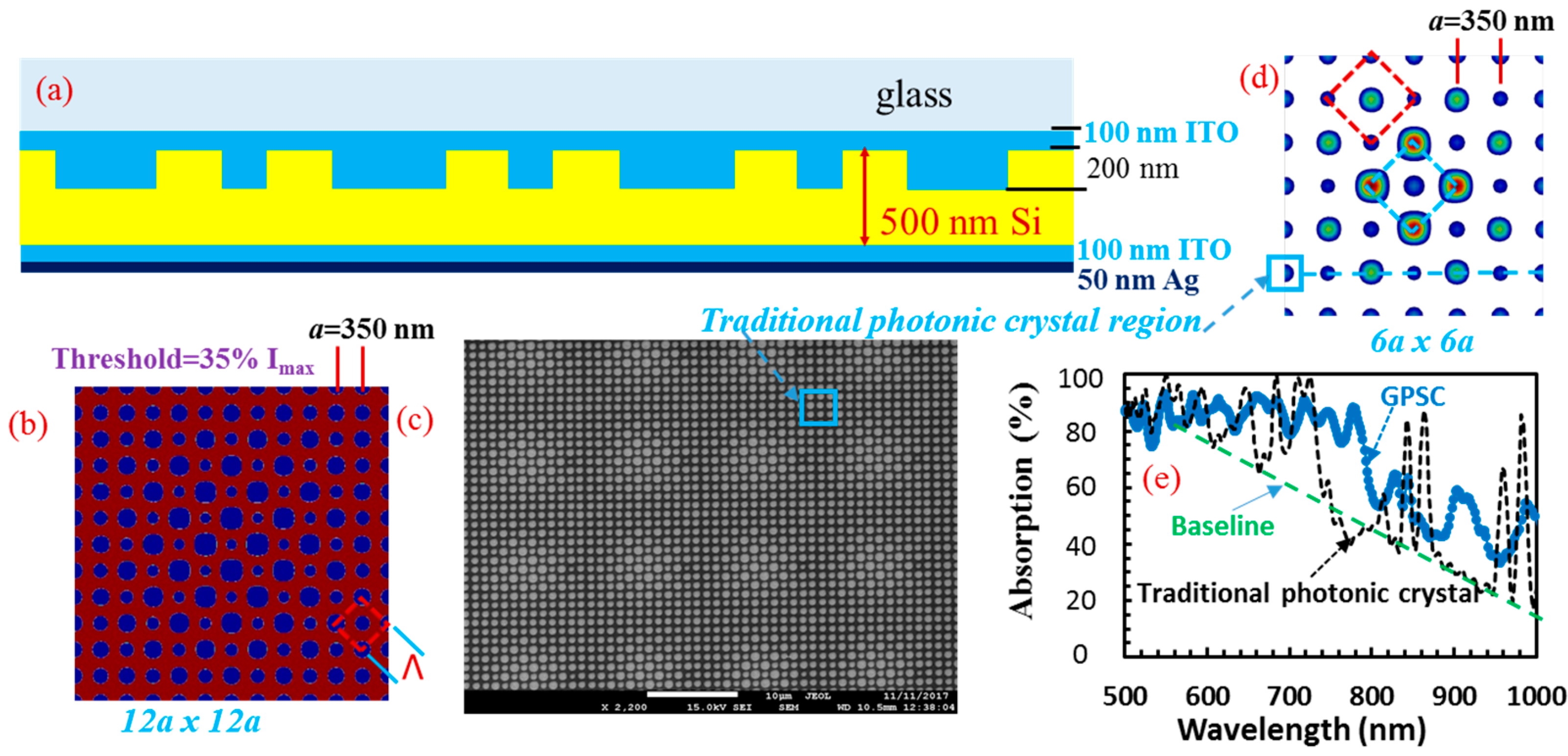
2. Description of Graded Photonic Super-Crystals and Simulation Methods
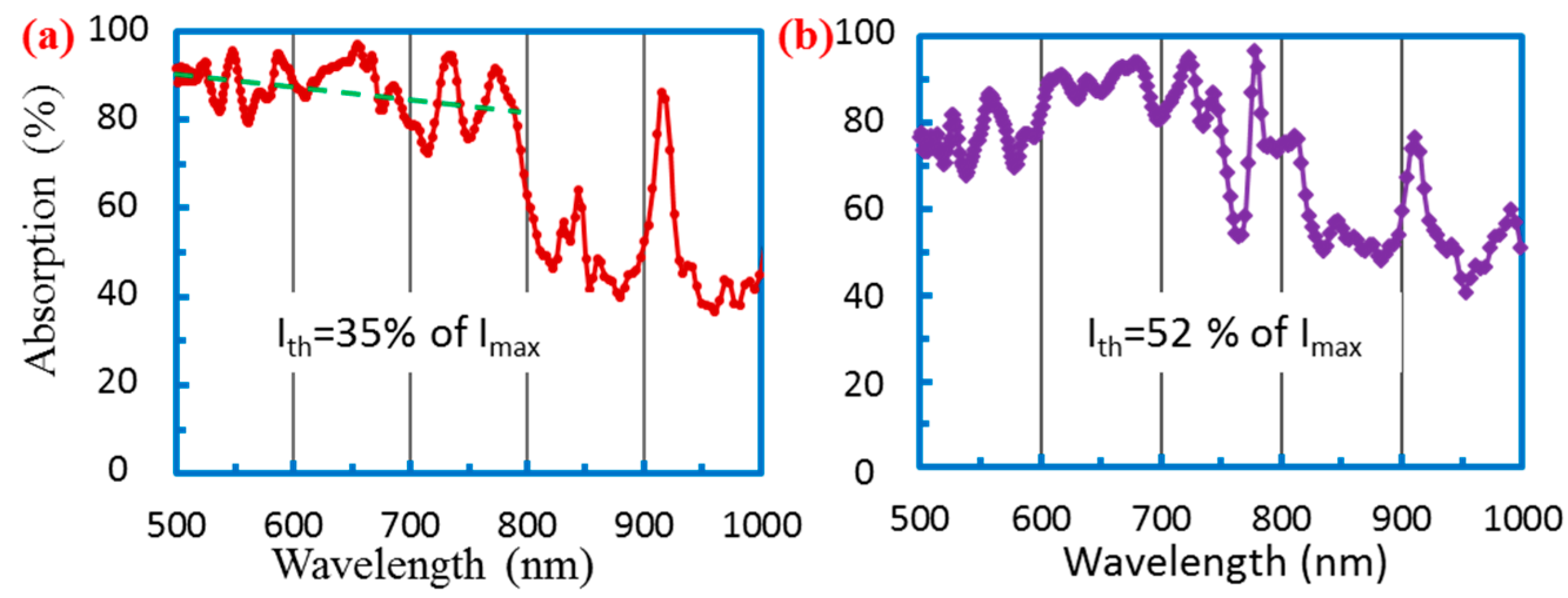
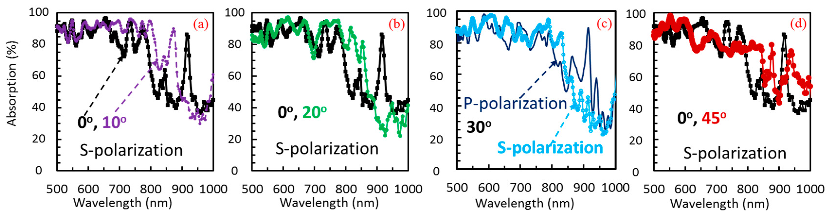
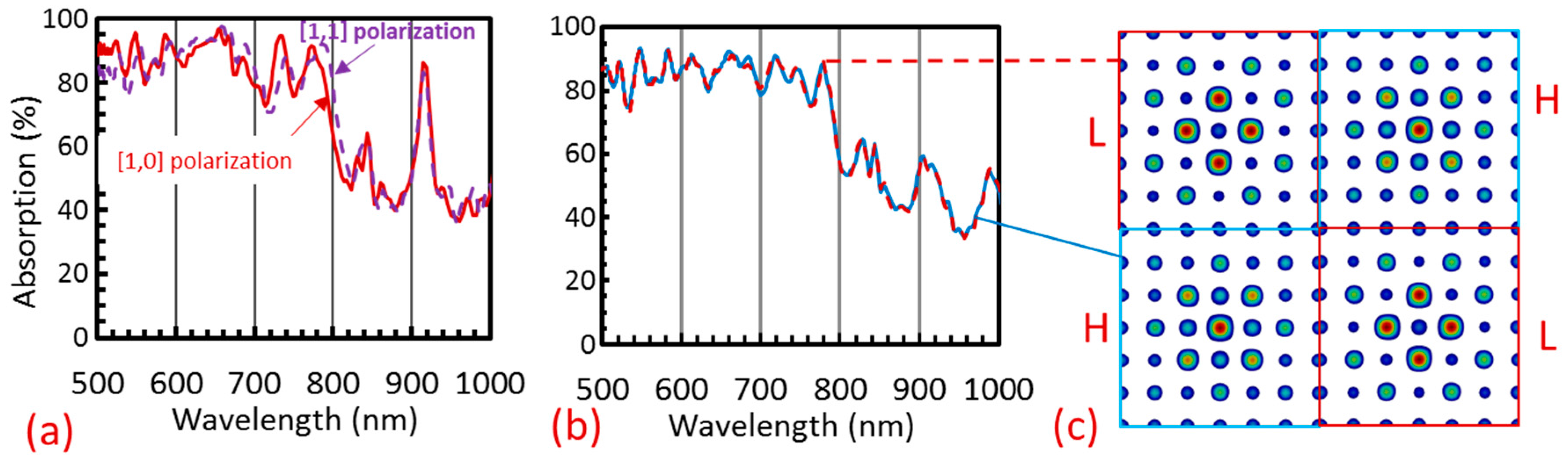
Using the results of Oskooi et al. [19] as a reference for comparison, similar solar cell structures to theirs were used in the simulations with the GPSC pattern instead of a disordered photonic crystal pattern. As shown in Figure 1a, a glass slide covered with a 300 nm layer of indium-tin oxide (ITO) (n = 1.8) was spin-coated with a positive resist, then patterned with the newly discovered GPSC [25,26], as shown in Figure 1b, and finally etched to a depth of 200 nm. A gold film was then deposited, and the positive resist was lifted off. The gold film initiated silicon growth for 200 nm (filling the groove of the pattern) [27]. Gold was again deposited over the entire flat surface to initiate the silicon film growth to a thickness of 300 nm. The gold film was then etched away. A 50-nm-thick silver film was deposited as the metal back-reflector following 100 nm ITO deposition.
The lattice constant, a, was used to describe the feature size of the nanostructure as shown in Figure 1b for a 12a × 12a unit super-cell of a GPSC. If the parameter a is less than 500 nm, electron-beam lithography can be used for the fabrication GPSC pattern. An SEM of a fabricated GPSC using electron-beam lithography in the positive resist PMMA is shown in Figure 1c. When the lattice constant is above 500 nm, eight-beam interference lithography (four inner beams with an interference angle of α and four outer beams with an interference angle of β) can be used to fabricate the pattern [26,27]. A GPSC with a unit super-cell size of 26a × 26a (with a = 1100 nm) has been fabricated using eight-beam interference [27]. The unit super-cell size can be controlled by the selection of angles α and β [27]. It is easier to fabricate a GPSC with a large unit super-cell than one with a small unit super-cell. However, it is difficult to have a high resolution simulation for a GPSC with a large unit super-cell. We expect that a GPSC with a unit super-cell of 12a × 12a can be achieved with experimental fabrication and high resolution simulation. The authors acknowledge that the lattice constant, a, is not in the right range; however, this paper focuses on the simulations only. The experimental results will be published in the future when a GPSC with the desired structural parameters has been fabricated and characterized.
In the simulation, the eight-beam interference patterns were converted to binary complex dielectric structures by comparing the interference intensity, I(r), with a threshold intensity, Ith (as a percentage of maximum intensity), using the following step functions: complex dielectric material = silicon, when I < Ith, and complex dielectric material = ITO when I > Ith. A complex dielectric function of amorphous silicon should be used. However, the complex dielectric function of amorphous silicon depends on the growth conditions [28], and no tabulated data was found. Furthermore, we determined the difference in structural resonance between silicon patterned with a GPSC and silicon patterned with a conventional photonic crystal. The selection of optical parameters of silicon had fewer effects on the resonance peaks than the structural parameters of the photonic crystals. Here we used tabulated data of the optical properties (refractive index and extinction coefficient) of crystalline silicon from 250 to 1000 nm [29]. Nano-structuring of silicon using GPSCs and conventional photonic crystals show little difference in improving light trapping in the high absorption region. Thus, the simulations are presented in the wavelength range between 500 and 1000 nm. Figure 1b shows a permittivity structure output that was used to check the accuracy of the simulation program in MEEP.
The simulations of absorption fraction in silicon patterned with the GPSC and conventional photonic crystal were performed using MIT’s open-source finite-difference time-domain (FDTD) software tool [30] via the Simpetus Electromagnetic Simulation Platform in Amazon Web Services (AWS). Due to the large unit super-cell size, 36-core virtual machines in AWS were selected for parallel computations. For a unit super-cell size of 12a × 12a, a resolution as large as 22 can be used corresponding to an estimated mesh size of 350/22 = 15.9 nm (about 1/31 of 500 nm light wavelength). For an accurate comparison of the silicon patterned with the GPSC and conventional photonic crystal, a unit super-cell size of 6a × 6a as shown in Figure 1d and a resolution as large as 40 was used corresponding to an estimated mesh size of 350/40 = 8.8 nm. For the structure in Figure 1a with a silver layer as a reflector, the transmission T(λ) is zero. In the simulation, only the reflection R(λ) was calculated and plotted. Using A(λ) = 1 − T(λ) − R(λ), the absorption was obtained. An integrated absorption can be calculated using the tabulated AM 1.5G solar spectrum. However, this was not done so as to compare the results with others under the same conditions [19,20]. Sunlight is almost unpolarized. To explain simulations, only the average values of the simulations with incident light polarized in the [0, 1] and [1, 1] directions are usually displayed, but in this study we chose to display them separately to analyze the polarization effects, which is one of the distinguishing features of the silicon patterned with GPSC.

3. Results

Figure 1d shows the GSPC with the unit super-cell of 6a × 6a (a = 350 nm) formed by eight-beam interference. The highest absorption occurs for the interference pattern with a threshold intensity at 30% of the maximum intensity. Figure 1e shows the absorption of 500-nm-thick silicon patterned with the GPSC with the unit super-cell of 6a × 6a and with an Ith value at 30% of the maximum intensity. The absorption from 500-nm-thick silicon patterned with a conventional photonic crystal is also shown in Figure 1d for comparison. The conventional photonic crystal is a square lattice with a uniform pattern (without a gradient structure), as indicated by the blue square outline in Figure 1c. We picked up a pattern (as indicated by a solid blue square) near the edge of the GPSC and measured the diameter of the pattern in Figure 1d. For the conventional photonic crystal, we used silicon with a unit cell size of 350 × 350 nm2 with circle-shaped ITO with a 145 nm diameter in the center. Comparing both spectra, (a) the absorption in silicon patterned with the conventional photonic crystal shows relatively sharp Bloch-mode resonance peaks, while the absorption spectrum from the silicon with the GPSC shows smoothed Bloch-mode resonance peaks, similar to the spectra of silicon patterned with a photonic crystal with 3.6% positional disorders in Figure 2 of [19]; (b) despite the overall decreasing absorption baseline with increasing wavelength as indicated by the dashed green line in Figure 1e and that in [19] by Oskooi et al., the absorption in Figure 1e for silicon patterned with the GPSC was kept at a high level, between 500 and 780 nm (i.e., broadband). The broadband light coupling can be understood by Equation (1) [31]:
2 π λ n e f f 2 π λ sin ( θ ) = G
where neff is the effective refractive index of the GPSC, λ is the wavelength in free space, and G is the reciprocal lattice vector. G can be 2π/a, 2π/Λ, 2π/(na) as defined in Figure 1b, or others. Λ = 2 a is the periodicity in the 45° direction relative to the x- or y-axis, and na (n is an integer number) is the length of the large unit super-cell, e.g., 6a.
The effective refractive index is defined as follows:
n e f f = f × n I T O + ( 1 f ) × n s i l i c o n
where nITO is the refractive index of ITO, nsilicon is the refractive index of silicon, and f is the fill fraction of ITO in the GPSC.
The GPSC consists of two sets of graded lattices. The dashed squares in Figure 1d link the corner lattices that belong to one set of the graded lattices. For example, the lattice dots linked by the dashed blue square in Figure 1d have a large circle in the center and gradually decrease their sizes in toward the edge of the unit super-cell. The two sets of graded lattices have the same periodicity; thus, the G parameter in Equation (1) is the same. However, the fill fraction f is spatially varying. For example, f = 13.5% for a circle of ITO with a 145 nm diameter in a 350 × 350 nm2 square of silicon at the left side of the dashed blue line, while f = 8.9% for a 350 × 350 nm2 square region in the middle of the line. Due to the availability of different fill fractions, light wavelengths in a broad range can meet the condition in Equation (1). Thus, broadband light-trapping enhancement is observed in the simulation for silicon with the GPSC due to the overlap of Bloch-mode resonances.
The degree of variation in the graded lattices depends on the location of the interference pattern, as described later in the discussion section, and on the size of unit super-cell. For GPSCs with a unit super-cell size of 12a × 12a, the corner areas in Figure 1b and the regions indicated by the solid blue square in Figure 1c have a uniform instead of graded lattice and behave as a conventional photonic crystal. The effect of the conventional photonic crystal can be seen in the absorption spectrum. For silicon patterned with a GPSC with a unit super-cell of 12a × 12a, a maximum average absorption occurs with an Ith value at 35% of the maximum intensity, as shown in Figure 2a. Broadband absorption and smoothed Bloch-mode resonance peaks still appear due to the graded regions of the pattern; however, the overall absorption decreases with increasing wavelength, as indicated by the dashed green line, due to the conventional photonic crystal regions. When the threshold intensity increases from 35% in Figure 2a to 52% in Figure 2b, fill fraction f decreases and neff increases. Therefore, based on Equations (1) and (2), and as shown in the figures, the wavelength for the overall absorption maximum is also red-shifted.
Figure 3 shows the dependence on incident angle for 500-nm-thick silicon patterned with a GPSC with a unit super-cell size of 12a × 12a (a = 350 nm) and a threshold intensity of 35% of the maximum intensity, for s-polarized light or [1, 0] polarization, with zenith angles of 10°, 20°, 30°, and 45° in Figure 3a–d respectively, and azimuth angles of 90° relative to the x-axis for all. Compared with the absorption spectrum at normal incidence (θ = 0°), the spectrum with the incident angle of θ = 10° shows a higher absorption, around 700 nm, a high broadband absorption region expanded to 800 nm, and a blue-shift of the Bloch-mode resonance peak around 900 nm. Except for a broader high-absorption region, which is expanded to 800 nm, the absorption spectra at 20° and 30° show almost the same light absorption as the one at 0°. At an incident angle of 45°, the simulated absorption decreases above 600 nm. Thus, under the wide-angle range of 30°, the absorption is almost the same. For p-polarization at a zenith angle of 30° in Figure 3c, the absorption peak around 900 nm still appears and the high absorption band is a little bit narrower than that with s-polarization.
Figure 4 shows the absorption of light with polarizations in the [1, 0] and [1, 1] directions incident on silicon patterned with the GPSC with a unit super-cell size of 12a × 12a, formed with the same threshold of 35% of the maximum intensity. We can see from Figure 4 that the absorption spectra are the same when the light is incident with different polarizations. In the [1, 1] direction of the GPSC, the lattice periodicity is larger, compared with that of the [1, 0] direction. The gradient filling fraction in the [1, 1] direction helps couple the light into the patterned structures, with an enhancement similar to that with [1, 0] polarized light, by meeting the conditions in Equations (1) and (2). Thus, we achieved polarization-independent broadband absorption when the silicon solar cell is patterned with the GPSC.
If the GPSC is formed by eight-beam interference as shown in Figure 4c, there are two “L” square regions where the central spot has a “low” intensity and two “H” regions where the central spot has a “high” intensity. If the unit super-cell is large, the “high” or “low” spot in the center is not critical as there are many lattice spots. However, the “high” or “low” spot in the center might become crucial in the absorption when the number of lattice spots become small. We simulated the absorption spectra for silicon patterned with GPSC with a unit super-cell size of 6a × 6a with formed with a threshold of 30% of the maximum intensity, as shown in Figure 4b. The absorption from the “H” region (dashed red line) is almost identical to that from the “L” region (blue line).

4. Discussion

For photovoltaic devices, nanostructuring the active layers has generated high local density of optical states in the absorber layer, allowing for more energy to be coupled into the solar cell and absorbed [10,11,12,13,14]. The appearance of many photonic bands, up to 144, below the photonic band gap or cavity mode [25] indicates a large density of optical states in the GPSC. When light is coupled into the structure, we expect resonance modes in the GPSC, waveguide modes in the horizontal plane in the silicon and ITO regions without GPSC, and leaky resonance modes in the vertical direction. In the simulations, light source detectors were placed everywhere in a region above the top-layer ITO. These detectors can collect signals in a large angle of up to 90°, but it cannot collect the waveguide modes mentioned above. In our simulations of the light extraction in organic light emitting diode devices [32], the fraction of light power in the waveguide modes is also zero. We have assumed zero reflection from waveguide modes in this study.
High resonance absorption and broadband optical response can be further studied via the optimization of iso-intensity surfaces of the interference pattern, lattice constant, and unit super-cell size. Figure 5a shows a cross section in the x–z plane of the interference pattern. When the sample is exposed at the location as indicated by the red line, the pattern will look like the one in Figure 5b, where the one set of lattice spots is smaller than the other. If the red line is shifted to the bottom of Figure 5a, the formed pattern will have a similar spot size in both sets of lattices. If the phases of the four outer interference beams were set to be (0, 0.15π, 0, 0.15π), the pattern in Figure 5b will become the one in Figure 5c.

5. Conclusions

The fraction of absorption of light in silicon solar cells, where the silicon is patterned with GPSCs, which are a hybrid of photonic crystals and disorder, has been simulated for the first time. Due to the spatially gradient fill fraction of dielectrics and the large number of available lattice constants in different directions, we obtained broadband, wide-angle, and polarization-independent absorption spectra. Broadband light-trapping enhancement is explained in terms of overlapping Bloch-mode resonances.

Acknowledgments

This work is supported by research grants from the U.S. National Science Foundation under Grant Nos. CMMI-1661842, 1661749, and ECCS-1407443.

Author Contributions

Y.L., S.H., and H.Z. conceived and designed simulations; S.H., D.L., M.A., and D.G. performed the simulations; Y.L., S.H., and D.L. analyzed the data; D.L. contributed parallel computation tools; Y.L. and S.H. wrote the paper. All authors read and commented on the manuscript.

Conflicts of Interest

The authors declare no conflict of interest. The founding sponsors had no role in the design of the study; in the collection, analyses, or interpretation of data; in the writing of the manuscript; or in the decision to publish the results.

References

  1. Atwater, H.; Polman, A. Plasmonics for improved photovoltaic devices. Nat. Mater. 2010, 9, 205–513. [Google Scholar] [CrossRef] [PubMed]
  2. Garnett, E.; Yang, P. Light trapping in silicon nanowire solar cells. Nano Lett. 2010, 10, 1082–1087. [Google Scholar] [CrossRef] [PubMed]
  3. Kelzenberg, M.D.; Boettcher, S.W.; Petykiewicz, J.A.; Turner-Evans, D.B.; Putnam, M.C.; Warren, E.L.; Spurgeon, J.M.; Briggs, R.M.; Lewis, N.S.; Atwater, H.A. Enhanced absorption and carrier collection in Si wire arrays for photovoltaic applications. Nat. Mater. 2010, 9, 239–244. [Google Scholar] [CrossRef] [PubMed]
  4. Brongersma, M.L.; Cui, Y.; Fan, S. Light management for photovoltaics using high-index nanostructures. Nat. Mater. 2014, 13, 451–460. [Google Scholar] [CrossRef] [PubMed]
  5. Bermel, P.; Luo, C.; Zeng, L.; Kimerling, L.; Joannopoulos, J. Improving thin-film crystalline silicon solar cell efficiencies with photonic crystals. Opt. Express 2007, 15, 16986–17000. [Google Scholar] [CrossRef] [PubMed]
  6. Hsu, C.M.; Battaglia, C.; Pahud, C.; Ruan, Z.; Haug, F.J.; Fan, S.; Ballif, C.; Cui, Y. High-efficiency amorphous silicon solar cell on a periodic nanocone back reflector. Adv. Energy. Mater. 2012, 2, 628–633. [Google Scholar] [CrossRef]
  7. Sai, H.; Fujiwara, H.; Kondo, M.; Kanamori, Y. Enhancement of light trapping in thin-film hydrogenated microcrystalline Si solar cells using back reflectors with self-ordered dimple pattern. Appl. Phys. Lett. 2008, 93, 143501. [Google Scholar] [CrossRef]
  8. Sai, H.; Saito, K.; Kondo, M. Enhanced photocurrent and conversion efficiency in thin-film microcrystalline silicon solar cells using periodically textured back reflectors with hexagonal dimple arrays. Appl. Phys. Lett. 2012, 101, 173901. [Google Scholar]
  9. Chutinan, A.; Kherani, N.P.; Zukotynski, S. High-efficiency photonic crystal solar cell architecture. Opt. Express 2009, 17, 8871–8878. [Google Scholar] [CrossRef] [PubMed]
  10. Mallick, S.; Agrawal, M.; Peumans, P. Optimal light trapping in ultra-thin photonic crystal crystalline silicon solar cells. Opt. Express 2010, 18, 5691–5706. [Google Scholar] [CrossRef] [PubMed]
  11. Bozzola, A.; Liscidini, M.; Andreani, L.C. Photonic light-trapping versus Lambertian limits in thin film silicon solar cells with 1D and 2D periodic patterns. Opt. Express 2012, 20, A224–A244. [Google Scholar] [CrossRef] [PubMed]
  12. Han, S.; Chen, G. Toward the lambertian limit of light trapping in thin nanostructured silicon solar cells. Nano Lett. 2010, 10, 4692–4696. [Google Scholar] [CrossRef] [PubMed]
  13. Sheng, X.; Liu, J.; Kozinsky, I.; Agrawal, A.; Michel, J.; Kimerling, L. Design and non-lithographic fabrication of light trapping structures for thin film silicon solar cells. Adv. Mater. 2011, 23, 843–847. [Google Scholar] [CrossRef] [PubMed]
  14. Park, Y.; Drouard, E.; El Daif, O.; Letartre, X.; Viktorovitch, P.; Fave, A.; Kaminski, A.; Lemiti, M.; Seassal, C. Absorption enhancement using photonic crystals for silicon thin film solar cells. Opt. Express 2009, 17, 14312–14321. [Google Scholar] [CrossRef] [PubMed]
  15. Callahan, D.M.; Horowitz, K.A.; Atwater, H.A. Light trapping in ultrathin silicon photonic crystal superlattices with randomly-textured dielectric incouplers. Opt. Express 2013, 21, 30315–30326. [Google Scholar] [CrossRef] [PubMed]
  16. Rinnerbauer, V.; Shen, Y.; Joannopoulos, J.D.; Soljačić, M.; Schäffler, F.; Celanovic, I. Superlattice photonic crystal as broadband solar absorber for high temperature operation. Opt. Express 2014, 22, A1895–A1906. [Google Scholar] [CrossRef] [PubMed]
  17. Rinnerbauer, V.; Lausecker, E.; Schäffler, F.; Reininger, P.; Strasser, G.; Geil, R.D.; Joannopoulos, J.D.; Soljačić, M.; Celanovic, I. Nanoimprinted superlattice metallic photonic crystal as ultraselective solar absorber. Optica 2015, 2, 743–746. [Google Scholar] [CrossRef]
  18. Hendrickson, J.; Guo, J.; Zhang, B.; Buchwald, W.; Soref, R. Wideband perfect light absorber at midwave infrared using multiplexed metal structures. Opt. Lett. 2012, 37, 371–373. [Google Scholar] [CrossRef] [PubMed]
  19. Oskooi, A.; Favuzzi, P.; Tanaka, Y.; Shigeta, H.; Kawakami, Y.; Noda, S. Partially-disordered photonic-crystal thin films for enhanced and robust photovoltaics. Appl. Phys. Lett. 2012, 100, 181110. [Google Scholar] [CrossRef] [Green Version]
  20. Oskooi, A.; De Zoysa, M.; Ishizaki, K.; Noda, S. Experimental Demonstrtion of Quasi-resonant Absorption in Silicon Thin Films for Enhanced Solar Light Trapping. ACS Photonics 2014, 1, 304–309. [Google Scholar] [CrossRef]
  21. Martins, E.; Li, J.; Liu, Y.; Depauw, V.; Chen, Z.; Zhou, J.; Krauss, T. Deterministic quasi-random nanostructures for photon control. Nat. Commun. 2013, 4, 2665. [Google Scholar] [CrossRef] [PubMed]
  22. Vynck, K.; Burresi, M.; Riboli, F.; Wiersma, D.S. Photon management in two-dimensional disordered media. Nat. Mater. 2012, 11, 1017–1022. [Google Scholar] [CrossRef] [PubMed]
  23. Rockstuhl, C.; Fahr, S.; Bittkau, K.; Beckers, T.; Carius, R.; Haug, F.-J.; Söderström, T.; Ballif, C.; Lederer, F. Comparison and optimization of randomly textured surfaces in thin-film solar cells. Opt. Express 2010, 18, A335–A342. [Google Scholar] [CrossRef] [PubMed]
  24. Ferry, V.E.; Verschuuren, M.A.; van Lare, M.C.; Schropp, R.E.I.; Atwater, H.A.; Polman, A. Optimized Spatial Correlations for Broadband Light Trapping Nanopatterns in High Efficiency Ultrathin Film a-Si:H Solar Cells. Nano Lett. 2011, 11, 4239–4245. [Google Scholar] [CrossRef] [PubMed]
  25. Lowell, D.; Lutkenhaus, J.; George, D.; Philipose, U.; Chen, B.; Lin, Y. Simultaneous direct holographic fabrication of photonic cavity and graded photonic lattice with dual periodicity, dual basis, and dual symmetry. Opt. Express 2017, 25, 14444–14452. [Google Scholar] [CrossRef] [PubMed]
  26. Nukala, P.; Sapkota, G.; Gali, P.; Philipose, U. Transport properties of Sb doped Si nanowires. J. Cryst. Growth 2012, 353, 140–144. [Google Scholar] [CrossRef]
  27. Lowell, D.; Hassan, S.; Adewole, M.; Philipose, U.; Chen, B.; Lin, Y. Holographic fabrication of graded photonic super-crystals using an integrated spatial light modulator and reflective optical element laser projection system. Appl. Opt. 2017, 56, 9888–9891. [Google Scholar] [CrossRef]
  28. Janai, M.; Allred, D.D.; Booth, D.C.; Seraphin, B.O. Optical properties and structure of amorphous silicon films prepared by CVD. Sol. Energy Mater. 1979, 1, 11–27. [Google Scholar] [CrossRef]
  29. Green, M. Self-consistent optical parameters of intrinsic silicon at 300 K including temperature coefficients. Sol. Energy Mater. Sol. Cells 2008, 92, 1305–1310. [Google Scholar] [CrossRef]
  30. Oskooi, A.F.; Roundy, D.; Ibanescu, M.; Bermel, P.; Joannopoulos, J.D.; Johnson, S. MEEP: A flexible free software package for electromagnetic simulations by the FDTD method. Comput. Phys. Commun. 2010, 181, 687–702. [Google Scholar] [CrossRef]
  31. Shi, J.; Pollard, M.E.; Angeles, C.A.; Chen, R.; Gates, J.C.; Charlton, M.D.B. Photonic crystal and quasi-crystals providing simultaneous light coupling and beam splitting within a low refractive-index slab waveguide. Sci. Rep. 2017, 7, 1812. [Google Scholar] [CrossRef] [PubMed]
  32. Hassan, S.; Lowell, D.; Yuankun, L. High light extraction efficiency in organic light-emitting diodes by patterning the cathode in graded superlattice with dual periodicity and dual basis. J. Appl. Phys. 2017, 121, 233104. [Google Scholar]
Figure 1. (a) Schematic of a silicon photovoltaic device patterned with a GPSC on a silicon (Si) absorbing layer. (b) Permittivity structures output from MIT Electromagnetic Equation Propagation (MEEP) simulation with a unit super-cell size of 12a × 12a (a = 350 nm, the red region is silicon and the blue region is ITO). (c) SEM of a fabricated GPSC in PMMA using e-beam lithography. (d) A unit super-cell size of 6a × 6a (a = 350 nm) formed by eight-beam interference with a threshold intensity Ith that is 30% of the maximum. (d) An eight-beam interference pattern with a unit super-cell of 6a × 6a (a = 350 nm). The dashed squares link lattices at corners that belong to one set of graded lattice. (e) Absorption spectra for silicon patterned with GPSC with a unit cell of 6a × 6a, and with a traditional photonic crystal with a unit cell size of 350 × 350 nm2 with silicon and a circle of ITO with a 145 nm diameter in the center. The dashed green line indicates the baseline of absorption for eye guidance.
Photonics 04 00050 g001
Figure 2. (a) Absorption versus wavelength profile at normal incidence for the silicon patterned with two GPSCs with a unit super-cell size of 12a × 12a: a GPSC of threshold intensity Ith = 35% (a) and a GPSC of threshold intensity Ith = 52% (b).
Photonics 04 00050 g002
Figure 3. (ad) Absorption spectra versus wavelength for 500-nm-thick silicon patterned with GPSC with a unit super-cell of 12a × 12a (a = 350 nm) and with a threshold intensity of 35% of maximum with [1, 0] polarized light at normal incidence, compared with the absorption spectrum at four off-normal angles of incidence (zenith angle = 10°, 20°, 30°, and 45°, respectively) with s-polarization. The absorption from the silicon patterned with the GPSC at an incident angle of 30° with p-polarization is also shown in (c).
Photonics 04 00050 g003
Figure 4. (a) Absorption spectra of light with polarizations in the [1, 0] and [1, 1] directions incident on silicon patterned with a GPSC with a unit super-cell of 12a × 12a (a = 350 nm), formed with a threshold of 35% of the maximum interference intensity. (b) Absorption spectra of light with polarizations in the [1, 0] direction incident on silicon patterned with a GPSC with a unit super-cell of 6a × 6a (a = 350 nm), formed with a threshold of 30% of the maximum intensity for the pattern from the L and H regions in (c). (c) Eight-beam interference pattern with a unit super-cell size 6a × 6a, showing two distinct regions, marked with an L (L for low intensity spot in the center) and an H (H for high intensity spot in the center).
Photonics 04 00050 g004
Figure 5. (a) Cross-section in the x-z plane of the eight-beam interference pattern. (b) Cross section in the x-y plane of the eight-beam interference patterned as viewed at the location indicated by the red line in (a). The pattern becomes the one in (c) when the phases of four outer interference beams are set to be (0, 0.15π, 0, 0.15π).
Photonics 04 00050 g005

