Review

Fabrication of 3D Photonic Crystals toward Arbitrary Manipulation of Photons in Three Dimensions

Department of Electronic Science and Engineering, Kyoto University, Kyoto 615-8510, Japan
*
Author to whom correspondence should be addressed.
Photonics 2016, 3(2), 36; https://doi.org/10.3390/photonics3020036
Submission received: 26 April 2016 / Revised: 28 May 2016 / Accepted: 30 May 2016 / Published: 3 June 2016
(This article belongs to the Special Issue 3D- and 2D-Nanofabrication for Photonic Devices)

Abstract

:
The creation of large-area, unintentional-defect-free three-dimensional (3D) photonic crystals in the optical regime is a key challenge toward the realization of the arbitrary 3D manipulation of photons. In this article, we discuss an advanced fabrication method of 3D silicon photonic crystals based on the highly accurate alignment and wafer bonding of silicon-on-insulator (SOI) wafers. We introduce an advanced alignment system, in which the alignment process is automated by image recognition and feed-back control of stages, and show that it achieves an alignment accuracy better than ~50 nm. The bonding of SOI wafers is also investigated to obtain 3D crystals composed of highly pure crystalline silicon. We show the fabrication results of large-area 3D photonic crystals based on such considerations and demonstrate the successful introduction of artificial defects as functional components, such as coupled waveguide pairs or waveguides/nanocavities. We expect that these will be pioneering results toward the arbitrary 3D control of photons using 3D photonic crystals.

Graphical Abstract

1. Introduction

The creation of three-dimensional (3D) photonic nanostructures in the optical wavelength regime is a key challenge for the arbitrary 3D manipulation of photons, including the control of emission or localization/propagation characteristics of photons without restrictions of directions and polarizations. In particular, the fabrication of 3D photonic crystals, which show wavelength-scaled 3D periodic variation of the refractive index and possess a complete photonic bandgap, has been intensively investigated [1,2,3,4,5,6,7,8,9,10,11,12,13,14] because they are expected to enable the arbitrary control of photons with the aid of embedded emitting materials and/or artificially introduced defects as functional photonic components. Thus far, various trial fabrications of such 3D structures toward the manipulation of photons in three dimensions have been performed [3,4,5,6,7,9,10,11,12]. However, it has been challenging to demonstrate well the effects of 3D photonic crystals, primarily because of the lack of advancements in the fabrication technology necessary for uniform and large-area 3D crystals as well as in the systematic design strategies for the arbitrary 3D control of photons. Nevertheless, several important milestones have been reached over recent years, including the control of light-emission phenomena [2] and realization of arbitrary 3D guiding of photons [13]. The application of new surface-related phenomena [8] has also been attracting much attention as a field connecting the inside and outside of 3D photonic crystals.
Further progress toward the arbitrary control of photons is expected on the basis of the abovementioned advancements. Although several types of approaches for 3D fabrications in this direction have been developed, which include methods based on the stacking of large-area 2D patterns of single-crystalline semiconductor by wafer bonding [1,15], the deposition of semiconductor layers and 2D processing [3,16], the stacking of small semiconductor pieces with 2D patterns by micro-manipulation [7,12], template-based depositions [4,6,11,17], self-assembly [18], and multi-directional deep etching by reactive ion etching [9,19,20] or ion-beam etching [21,22,23,24], a method that enables the fabrication of 3D photonic crystals satisfying the following criteria is demanded: (1) arbitrary large-area fabrication, (2) no unintentional defects, and (3) high design freedom for artificial defects. Considering these points, the method based on the stacking of large-area 2D patterns through a highly precise alignment and semiconductor wafer bonding process [1,15] is one of the most reliable candidates considering the advancements in the design and analysis of various functional elements, such as single-mode nanocavities, wide-band single-mode waveguides, concept of efficient coupling of waveguide pairs or waveguides/nanocavities, and control of input/output characteristics, in such stacked 3D photonic crystals [13,25,26,27,28,29].
In this article, we discuss the key technologies in such a 3D fabrication method. We describe in detail the performance of our advanced automatic, high-precision alignment system based on an image recognition and automatic feedback system [13], the alignment accuracy of which is better than ~50 nm in the x, y, and θ (rotational) directions. We also investigate Si-Si bonding by using silicon-on-insulator (SOI) structures toward the easy fabrication of high-quality and low-loss 3D photonic crystals. Finally, we introduce fabrication results for stacked-stripe 3D photonic-crystal structures and artificial defects. We expect that these will be pioneering results toward the arbitrary 3D control of photons.

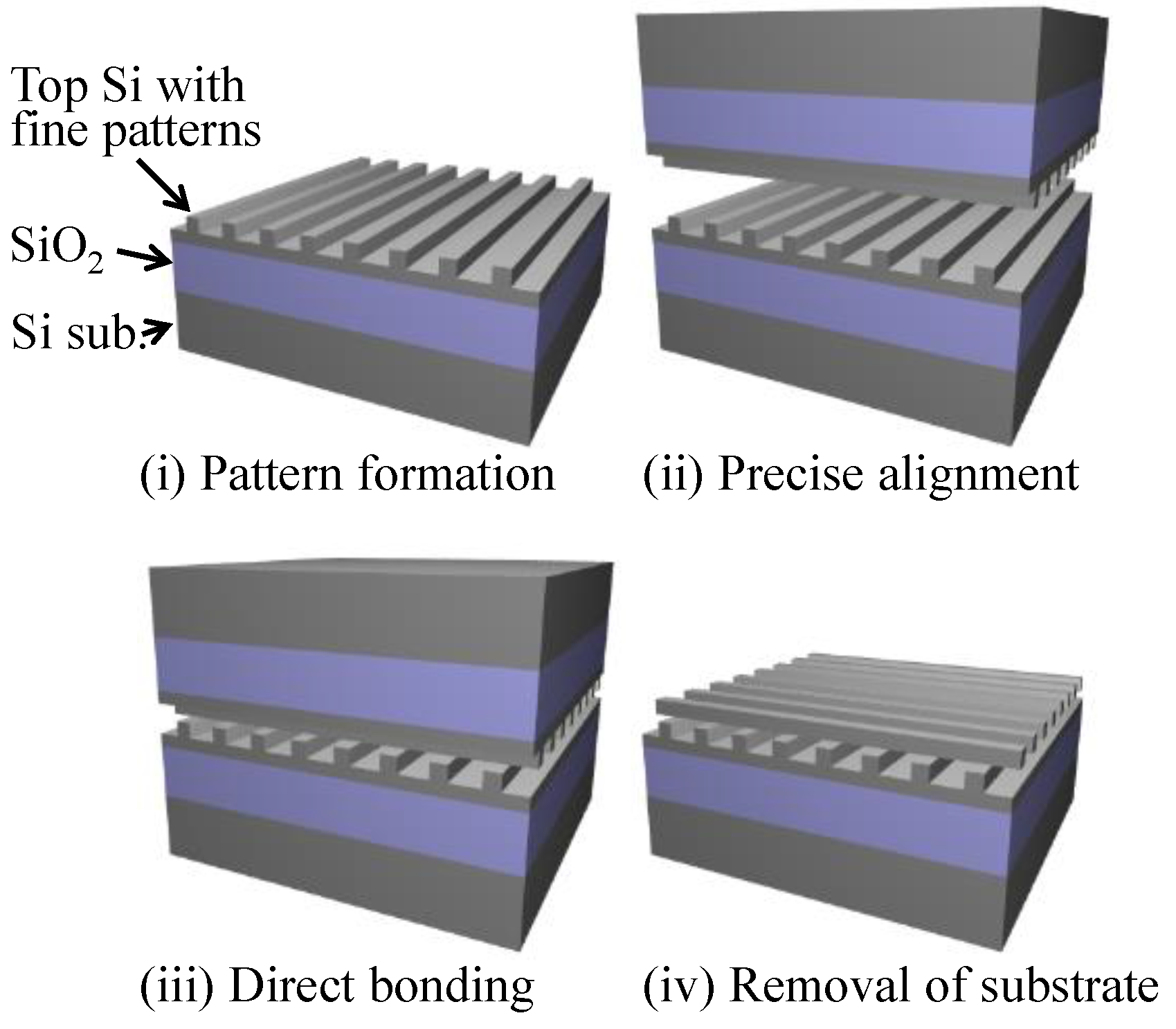
2. Automatic Alignment System for High-Precision Stacking of 2D Patterns

A schematic illustration of our fabrication process is shown in Figure 1. In this procedure, one of the most important processes is the alignment of stacking positions. From our numerical calculations, we found that the accuracy of the stacking position should be better than 0.1 periods of the parallel rods in the stacked-stripe structure to obtain a photonic-badgap effect close to that in perfect structure [30,31]. This requires a stacking accuracy of several tens of nanometers when considering operation in the optical-communications wavelength range, where the lattice constant is designed to be approximately 500–700 nm. However, commercially available wafer-to-wafer alignment and bonding systems only provide an accuracy of the order of micro- to submicro-meters [32,33]. Therefore, we have proposed an alignment method and bonding system for 3D photonic crystals.

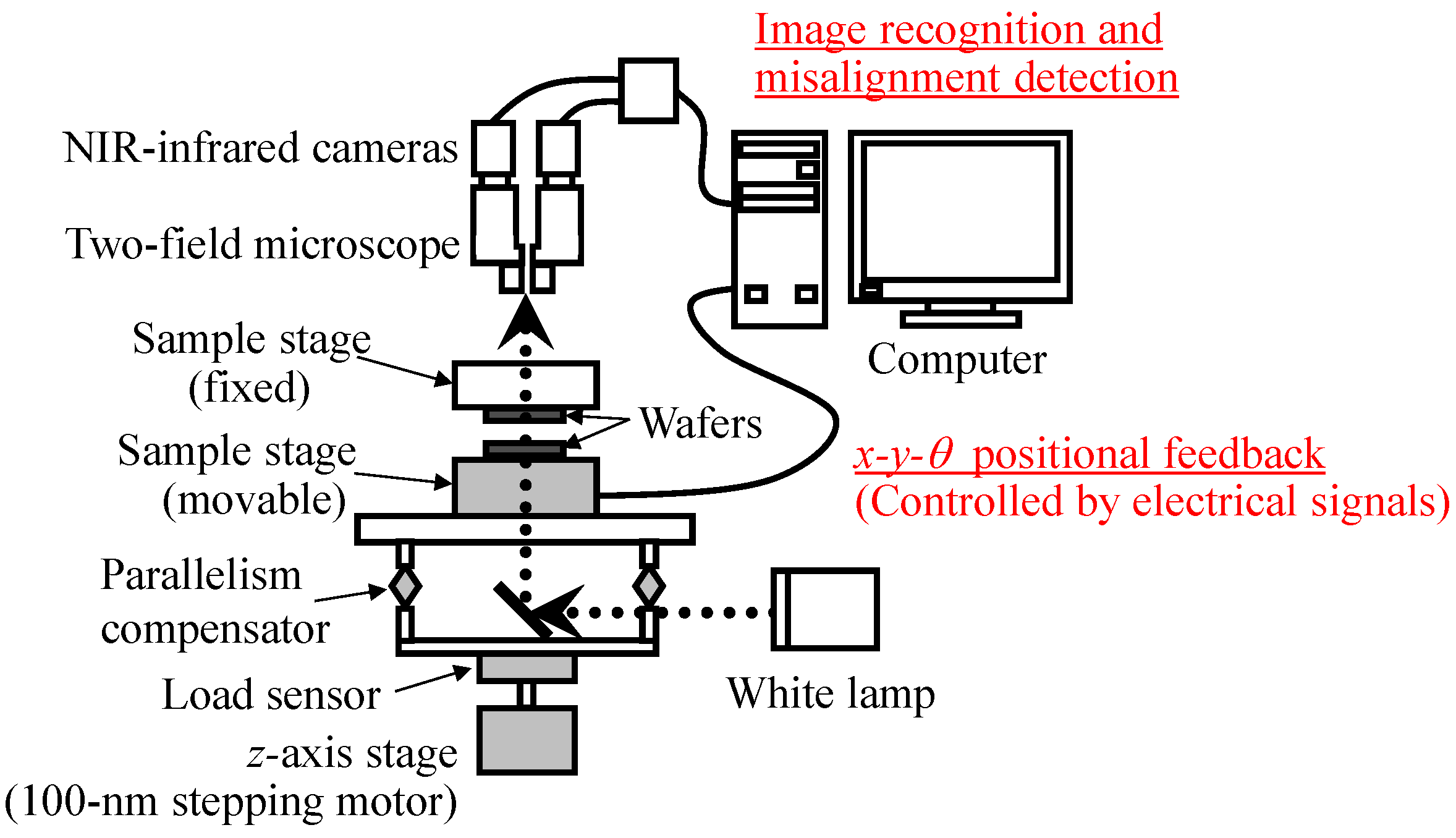
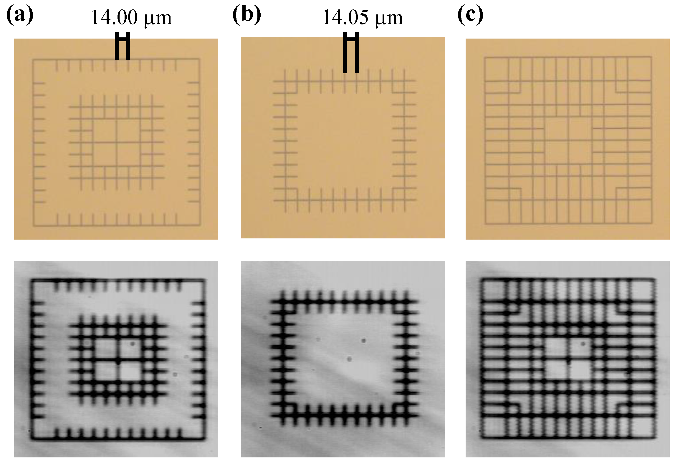
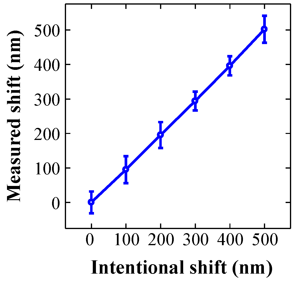
2.1. Misalignment Detection by Image Recognition Technique

Firstly, methods for detecting misalignments of the order of several tens of nanometers are important to improve accuracy. Our first approach was to observe laser diffraction patterns at the layered structure of periodic patterns [15]. In this laser-beam-assisted method, although the relative position of the layers could be determined, it was difficult to align the absolute position of the layers because of the periodic appearance of the same diffraction patterns. In addition, the diffraction patterns became complex when multilayered structures were aligned and stacked [34]. Subsequently, we employed a method using vernier-caliper markers [35] to obtain the absolute value of misalignment. This enabled precise alignment and bonding with an accuracy better than 100 nm through the improvement of the contacting equipment, such as the employment of a system for observing and compensating for the parallelism of two wafers and the introduction of contact (or load) sensors [35]. Nevertheless, as the evaluation of misalignment is based on human vision in this technique, it is not versatile. It is also noteworthy that the difficulty in the simultaneous observation of misalignment at two points in human vision has obstructed fine alignment in the rotational direction, which limits the applicable size of the photonic-crystal area.
Thus, we developed and demonstrated an automatic alignment system based on computer-aided image recognition and automatic positional feedback [13], which can be commonly used by anyone. Figure 2 schematically shows the overall configuration of the developed system. Two wafers are introduced in the system in a face-to-face configuration. To detect the amount of the misalignment between two wafers, we found the positions of alignment markers formed on two wafers by using the image-recognition technique, which is commonly used in the field of machine vision [36], and quantitatively estimated the misalignment from the distance between the centers of two markers on each wafer. Figure 3 shows typical images of the alignment markers; the upper and lower panels show the optical-reflection (visible) and optical-transmission (near-infrared) images, respectively. The markers were prepared on the target wafers (SOI wafers) by using electron-beam lithography and subsequent dry etching at the time of formation of photonic-crystal patterns to ensure the relative position between the alignment markers and photonic crystals. The width and depth of the etched pattern was ~800 nm and ~200 nm, respectively. Figure 3a,b shows the markers for wafers mounted on the upper and lower sides, respectively. Here, because the relative distance between two wafers is estimated by detecting these two markers, the markers are designed such that they do not overlap with each other. When we perform alignment, these two markers are overlaid, and we find their centers of gravity. For the purpose of correcting the detection system (and also checking the performance of detection misalignment), we also prepared a reference marker, as shown in Figure 3c, on one side of the wafer. Here, we improved the shape of markers such that they consisted of grating-like patterns. This suppresses the deviation of the readout value compared with that of simple patters such as squares or circles. It is also noteworthy that these markers have different spacings; one has a period of 14.00 μm, and the other has a period of 14.05 μm. When these markers are overlaid, they act as vernier calipers composed of a main scale and a vernier scale, the difference between the periods of which is 50 nm. This enables the visual observation of misalignment of the order of 50–100 nm [35], despite the use of illuminating light with a wavelength including 1100–1600 nm in the case of Si-based materials with an InGaAs near-infrared camera. This mechanism ensures the reliability of the computer-aided automatic detection of misalignment by human vision.
Figure 4 and Figure 5 show the misalignment-detection performance of the system. First, we evaluated the marker pattern shown in Figure 3c, which has no misalignment. In this demonstration, we found the central unit of the marker in Figure 3a and the whole part of the marker in Figure 3b, and obtained the distance between two markers. Figure 4a shows the detected amount of misalignment for 100 measurements. Each detection was performed with an interval of several seconds. As can be seen in Figure 4a, the readout value was stationary within a variation of about ±20 nm. The frequency histogram shown in Figure 4b indicates that the standard deviation σ is less than 11 nm (3σ < 32 nm). We then confirmed the performance of misalignment detection. For this purpose, we prepared two markers on one wafer by intentionally shifting their relative position in x-direction and then detected the amount of the shift. For each intentional shift, 25 measurements were performed. Figure 5 shows the experimental results of the average measured values and 3σ ranges. The average values were directly proportional to the known intentional shift. Figure 5 also indicates that the error detection could be maintained within a variation of readout values less than ~40 nm in 3σ, even when misalignment occurs and a small part of the two markers overlap with each other. This result implies that a deviation smaller than that detectable by human vision using a vernier caliper is successfully achieved by introducing an image-recognition technique.

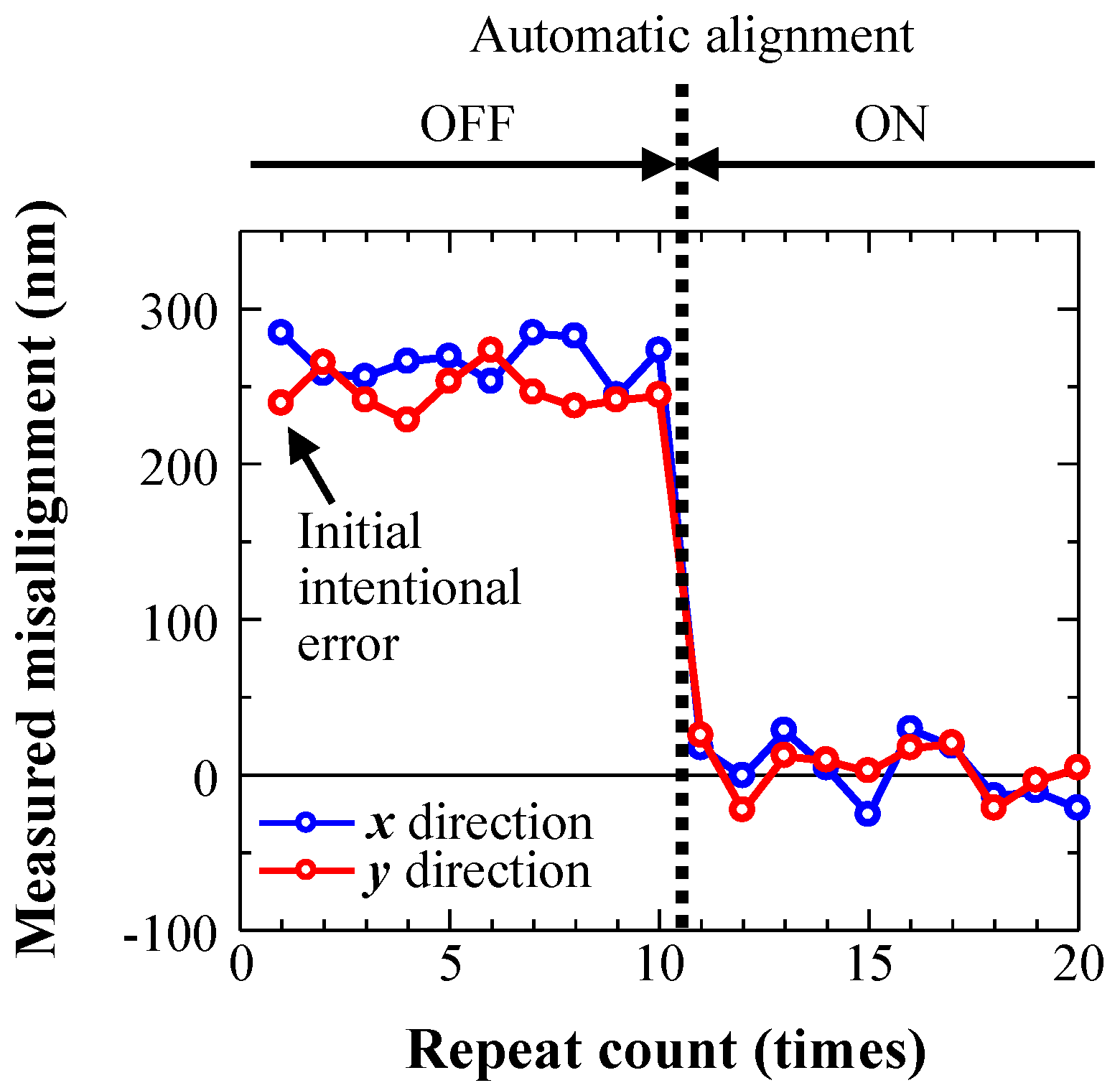
2.2. Automatic Correction of Misalignment by Feed-Back Control of Stages

Based on the obtained quantitative amount of misalignment, we automated the correction of misalignment by controlling the action of electrically driven stages. Regarding the driving components, electrically driven stages that allow motion with a resolution of < 1 nm in the in-plane (x, y) directions (piezo-electric actuators) and < 10 nrad in the θ direction are employed (stepping motor). In this study, we employed proportional feedback for the correction of misalignment; the stages were operated to move across a certain distance such that only the detected misalignment is cancelled out. However, it is noteworthy that piezo-actuators possess hysteresis characteristics; therefore, the correction may not be perfectly completed in only one step, and several steps may increase the accuracy of the correction.
Figure 6 shows the action of automatic positional feedback. Here, two wafers are mounted with a gap of ~3 μm. As the first step, the relative positions of the wafers were intentionally adjusted to include a misalignment of approximately 250 nm in both the x and y directions. After ten cycles without automatic correction, we turned on the automatic action, and the x- and y-directional stages were driven to cancel the detected positional misalignment by applying a voltage to a piezo-actuator. In Figure 6, it is apparent that the misalignment is successfully corrected in only one or two steps. The residual misalignment reached a value less than 50 nm, and unanticipated divergence was completely absent. Here, because the readout value showed a deviation, the positional correction should include deviations greater than the deviation only in the readout (twice in maximum). We expect that this deviation should be easily suppressed by employing the appropriate proportional-integral-derivative (PID) control of stages.
We also applied this automatic feedback for the correction of rotational error in the θ direction by the feedback to the rotational stage. For this purpose, we used two-field microscopy (Figure 2), the distance of which can be varied, to enable the simultaneous observation of two separated areas, which was difficult in the previous detection technique based on human vision. With two-field microscopy, stacking accuracy can be ensured in a large area by increasing the interval between the two markers d; in simple terms, the rotational error σθ is approximated as σθ ~ 2 σx,y/d, where σx,y is the error in the x- and y-directions. Eventually, one round of overall estimation and correction of misalignment (x, y, and θ) was completed in several seconds, which is a sufficiently short time compared with the time taken for manual alignment. In the actual bonding process, we gradually brought the wafers together with a step of 100 nm while repeating the detection and correction of misalignment, and we finally made the wafers come into contact with each other. The fabrication results of 3D photonic crystals are described later.

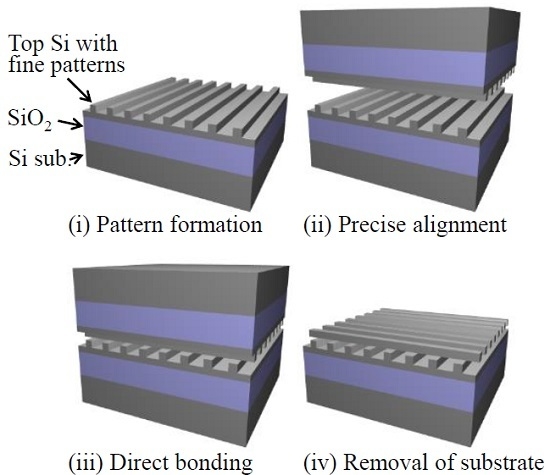
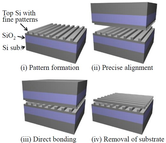
3. Wafer Bonding of Silicon-on-Insulator Structure for 3D Stacking

We subsequently investigated the bonding of 2D patterns prepared on single-crystalline silicon (Si). The direct wafer-bonding technique of semiconductors has been an important basis for the fabrication of 3D photonic crystals. We have successfully demonstrated a variety of wafer-bonding techniques, which include not only the homogeneous bonding of indium phosphide (InP) or gallium arsenide (GaAs) [1,5,8] but also the heterogeneous bonding of InP/GaAs [2,37] or InP/Si [9] for the integration of emitting materials into the 3D photonic crystal. Here, when considering the simplification of the fabrication process and the usage of high-quality materials showing less unintentional optical absorption, crystalline Si is an important candidate as the composite material of 3D photonic crystals. Actually, the highest Q-factor of nanocavities achieved thus far has been in two-dimensional (2D) Si photonic crystals [38], which suggests the usefulness of Si for high-performance photonic crystals. Because it is necessary to repeat the alignment and stacking process, the SOI structure, which possesses a sacrificial SiO2 layer, is useful to fabricate 3D photonic crystals based on Si. However, the bonding of SOI/SOI structures is difficult [35,39] because the SOI structure originally possesses internal stress and the resulting warpage [40]. There is concern that such stress tends to introduce a gap in the bonded interface of 3D photonic crystals because the contacting area per unit area of 3D photonic crystals becomes small (typically less than 10%), weakening the bonding strength. Therefore, we investigated the wafer bonding condition of SOI/SOI structures in detail by comparing the analytical results obtained using the 2D finite-element method (FEM) with experimental results.

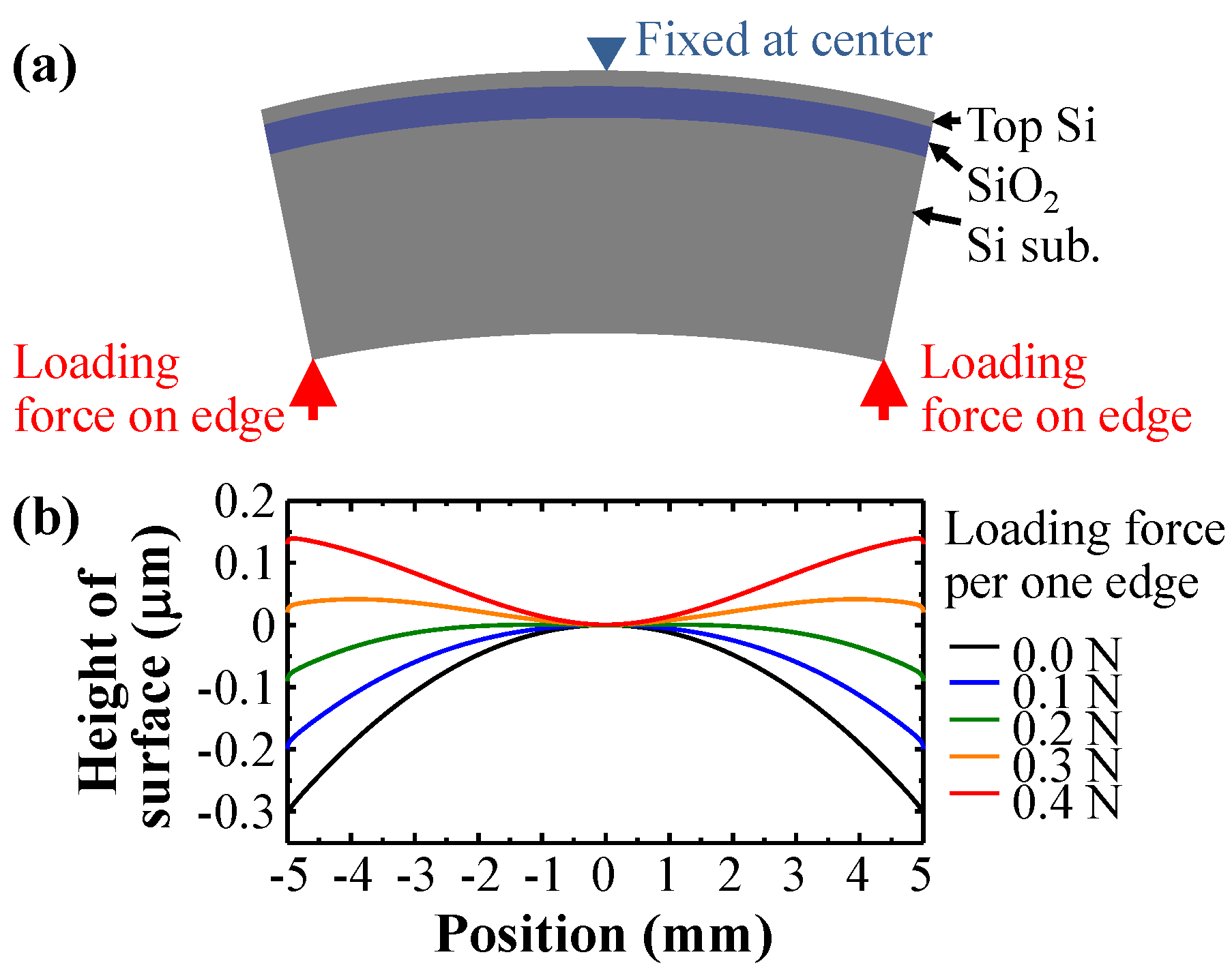
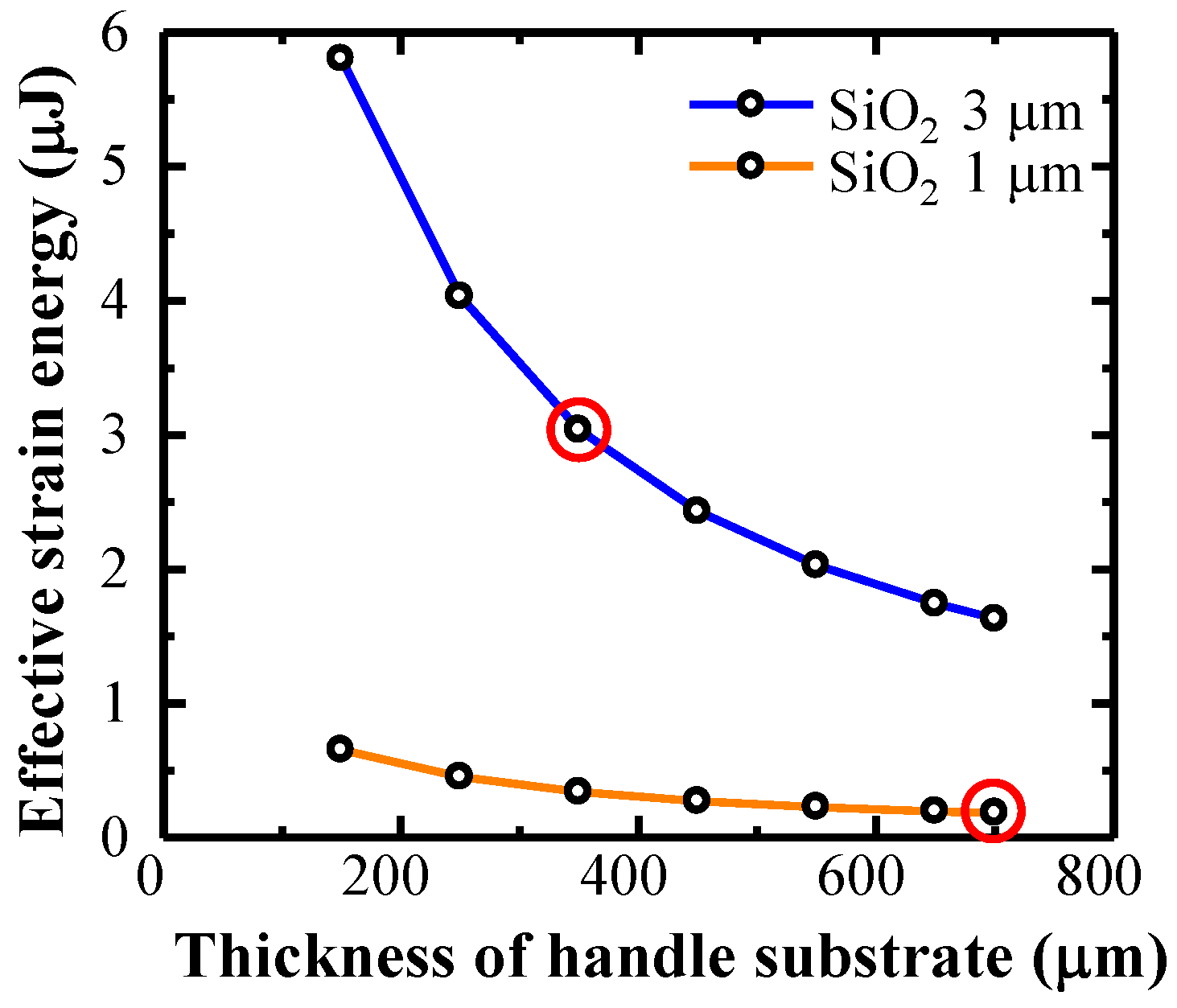
3.1. Analysis of Strain in SOI Structure

In the bonding process, we first obtain room-temperature bonding based on hydrogen bonding to keep the finely aligned position and then thermally anneal the bonded wafers for increasing the bonding intensity. In this sequence, it is highly important to obtain sufficient room-temperature bonding to maintain high accuracy. Therefore, we considered the influence of the strain energy in bonded SOI/SOI structures to obtain uniform bonding at room temperature. Here, SOI wafers generally possess warpage owing to their fabrication process; the SOI structure is typically fabricated by bonding Si and SiO2 (or SiO2 and SiO2 formed on Si) at high temperatures such as 1400 K [41], and the internal stress is accumulated and warpage is induced at room temperature owing to the difference between the thermal expansion coefficients of Si and SiO2.
Figure 7 shows the calculated effective strain energy of bonded SOI/SOI structures with several thicknesses of the buried SiO2 layer and handle Si substrate. We used 2D FEM for the calculations. The thickness of the top Si layer was fixed to 700 nm. The width of SOI wafer was set as 10 mm. The depth was also considered to be 10 mm. The effective strain energy is defined as the difference between the total strain energy of the bonded SOI/SOI structure and that of two separated SOI wafers. Here, we consider the case of un-patterned flat SOI wafers. The following material parameters were used in the calculation: the thermal expansion coefficients of Si and SiO2 are 4.0 × 10⁻⁶ K−1 and 4.8 × 10⁻⁷ K−1, respectively, and the Young’s moduli and Poisson’s ratios were 130 GPa and 0.28 for Si and 72 GPa and 0.17 for SiO2, respectively. The result shown in Figure 7 clearly indicates that the thickness of the buried SiO2 layer strongly influences the effective strain energy. Furthermore, it can be found in Figure 7 that the effective strain energy is proportional to the square of the SiO2 thickness.
When considering sufficient room-temperature bonding, this effective strain energy should be less than the bonding energy; if not, the contacted wafers are gapped. The experimentally estimated effective bonding energy of the room-temperature bonded interface of hydrophilic Si/Si is reported as ~100 mJ/m2 in air and ~20 mJ/m2 in water [42]. When considering both the width and depth of SOI wafers as 10 mm, the total effective surface energy of a pair of Si wafers in air and water is estimated to be ~20 μJ and 4 μJ, respectively. By comparing this value with the analytical result shown in Figure 7, it is important that the effective strain energy in the bonded SOI/SOI structure including the 3-μm-thick SiO2 layer is in the same range as the effective surface energy in water, and in the case of the SOI wafers with 1-μm-thick SiO2, the effective strain energy is suppressed to be one order less than the effective surface energy for the case in which sufficient bonding is expected even when the photonic crystal patterns are introduced and the contact area is reduced.

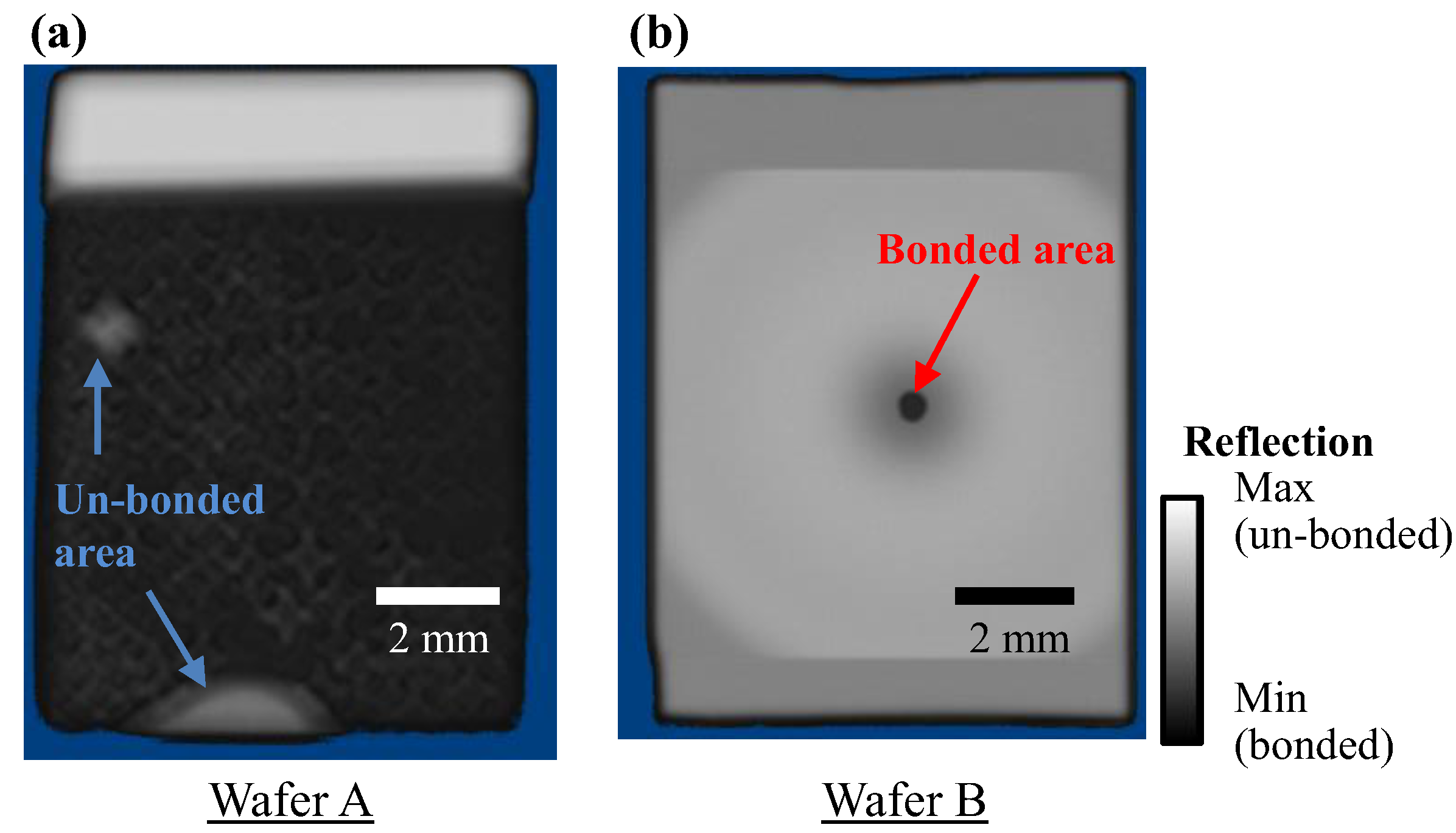
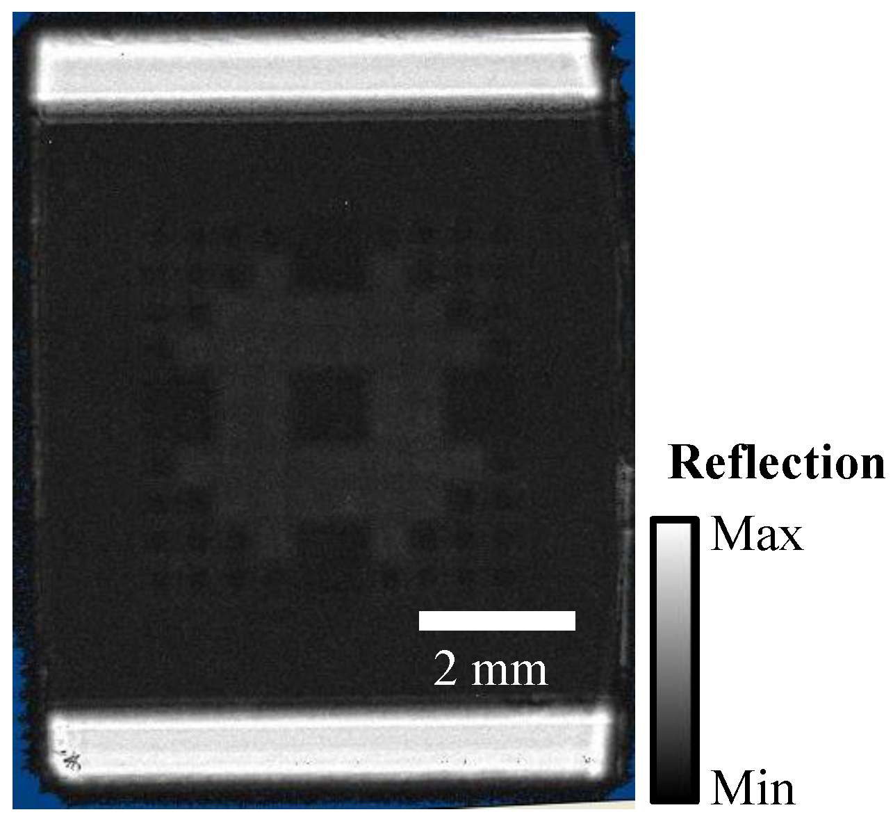
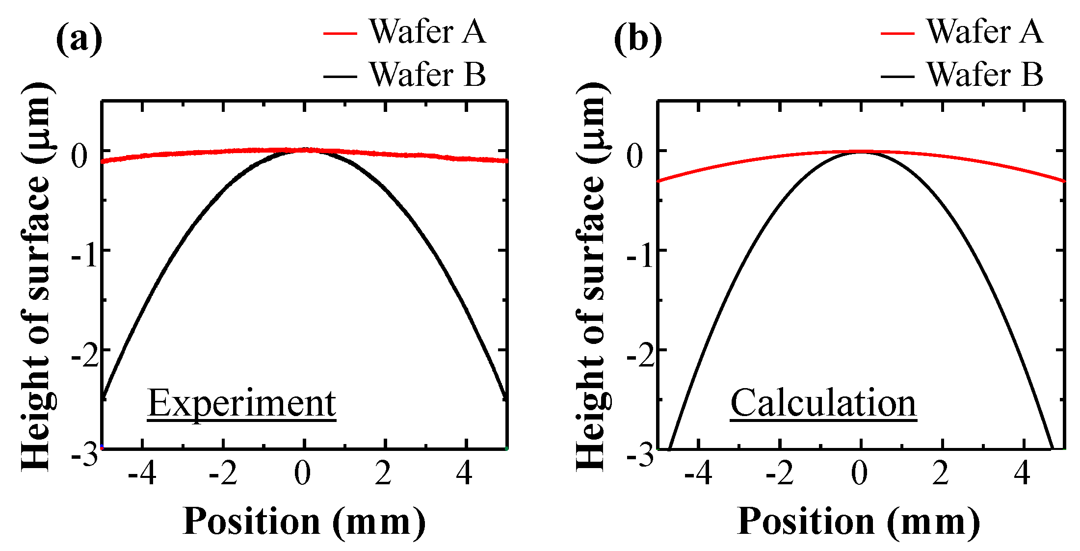
3.2. Experimental Bonding of SOI Wafers

To confirm these numerical results, we experimentally investigated the room-temperature bonding of un-patterned SOI wafers. We prepared two types of SOI wafers with different thicknesses of the Si-top, buried SiO2, and handle substrate layers. The basic parameters are listed in Table 1. The wafers had a size of approximately 10 mm × 10 mm. First, we measured the warpage of the SOI wafers by using a contact-type profilometer (Figure 8a) and compared it with the calculation result by 2D FEM (Figure 8b). It is clear that the wafer with a thicker SiO2 layer possess greater warpage, which agrees with the calculation results. To obtain the full-area contact of two wafers, we subsequently estimated the necessary loading force. Figure 9 shows the model and calculation result of wafer A with the loading force at the edge. The result suggests that wafer A requires a loading force of approximately 0.3–0.5 N per edge to be flattened. Therefore, a loading force of 1.2–2.0 N (or four-fold load in each edge) is expected to make the two wafers flat and keep them in contact with each other in the full area.
Subsequently, we prepared SOI wafers with hydrophilic surface treatment and performed room-temperature bonding. We brought the pair of SOI wafers in contact with other and flattened them by adding a loading force of 2.5 N. After waiting for 1 h to saturate the room-temperature bonding strength, we evaluated the obtained bonding area through scanning acoustic microscopy (SAM) in water. This measurement enables the nondestructive observation of the gap between the wafers by monitoring the intensity of the ultra-sonic waves reflected at the bonded interface. Figure 10a,b shows the SAM images taken for the bonded SOI/SOI interface of wafers A and B, respectively. As shown in Figure 10a, the SAM image of wafer A shows a uniform pattern, except for the white area, which is less than 5% of the total area. On the other hand, the SAM image of bonded wafer B shows a strongly nonuniform pattern (Figure 10b). Here, the white area indicates that the reflection of the ultra-sonic wave is strong; we can find that a gap is formed in this white area. Note that the white areas around the top and bottom of the wafers are artifacts due to the difference of the sizes of bonded wafers and do not indicate debonding. These results experimentally demonstrate that wafer A was successfully bonded in almost the entire area and that, in contrast, most of the area of wafer B was debonded because of the large strain energy. The results clearly indicate the validity of the FEM calculations discussed above.

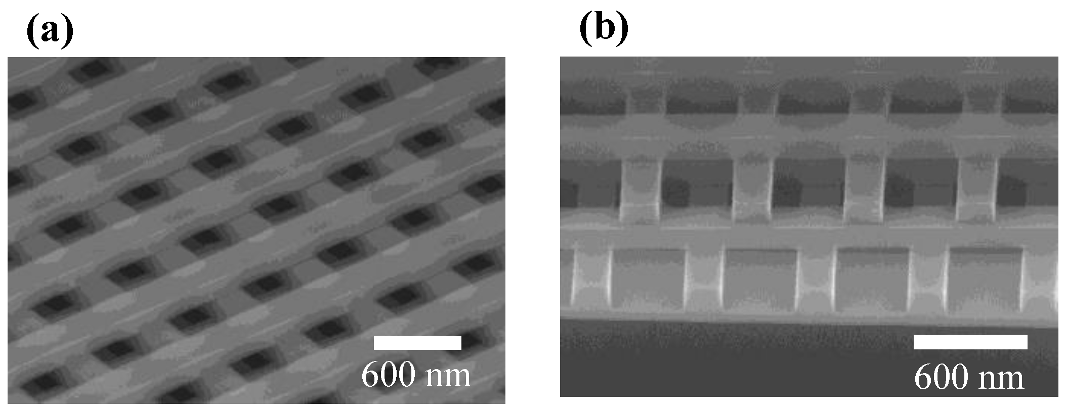
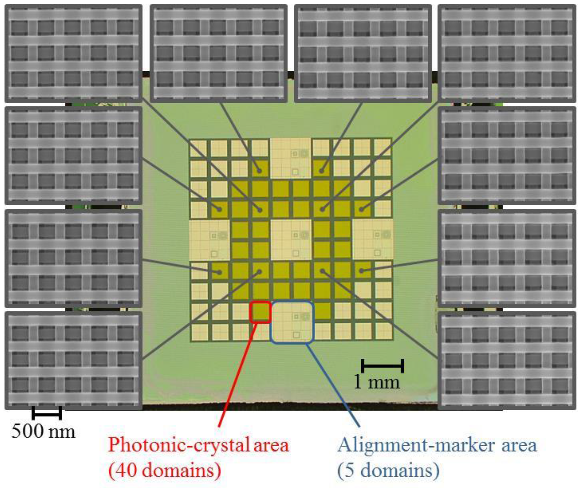
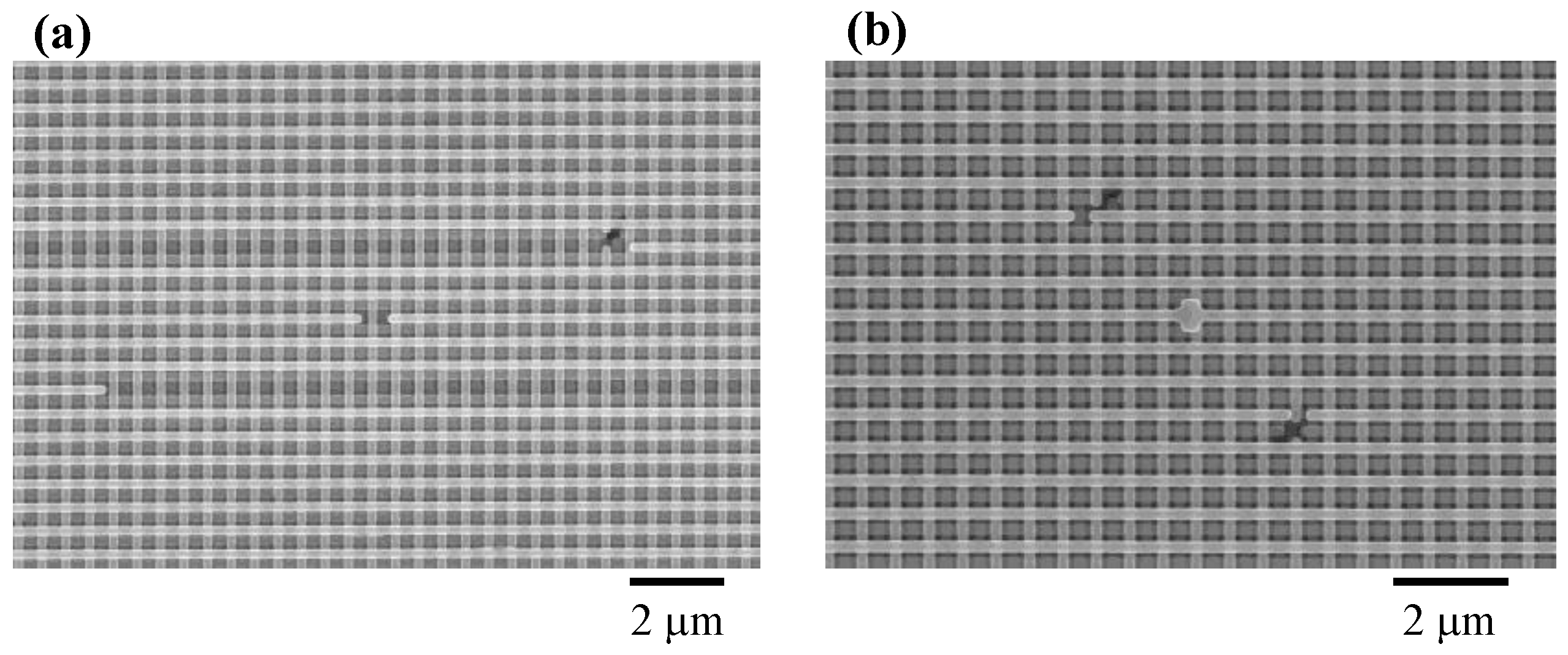
4. Fabrication of 3D Photonic Crystals

Finally, we show the actual fabrication of 3D photonic crystals based on the above investigations of automatic alignment and SOI/SOI bonding. We used SOI wafer A with a size of 10 mm × 8 mm and arrayed 40 domains of photonic-crystal areas, each occupying an area of 400 μm × 400 μm. On this wafer, we prepared five domains for alignment markers; two are for the actual alignment in the x, y, and θ directions, and the others are spare markers.
Figure 11 shows the SAM observation result of the wafer with photonic-crystal patterns and alignment markers. The image was taken after final annealing of bonded wafers at 1450 K in an argon atmosphere. This figure indicates that the entire sample area is successfully bonded. The photonic-crystal area has a grey color because of the existence of an air/Si periodic structure; the filling factor of air is ~70%. After the bonding, we selectively removed one side of the handle Si substrate and buried SiO2 and residual thin-Si layer by dry etching and chemical etching processes. After repeating such a procedure thrice, we obtained a 4-layered structure. Figure 12 shows a typical scanning electron microscope (SEM) image of the stacked stripe structure. As shown in Figure 12, silicon bars are stacked as expected without debonding while maintaining the sharp cubic shape. This suggests that the control of internal stress in SOI wafers by the adequate choice of layered structure enabled successful bonding even in the 3D architecture with a small contacting area.
Figure 13 illustrates the in-plane accuracy of the stacking position in the entire area. Here, the in-plane period was set to be 500 nm, and both the width and height of the rods were designed to be 180 nm. An optical-microscope image of the entire sample is shown in the center of Figure 13. The orange regions are the areas of photonic crystals. The regions surrounded by blue boxes are markers for alignment. The SEM images of each photonic-crystal area are shown around the optical-microscope image. These SEM images show that highly precise alignment was achieved in all the photonic-crystal regions on one chip. Although the formation of these four-layered structures requires the alignment and stacking procedure to be repeated thrice, all of the crystals were constructed with misalignments of less than ~50 nm. These results demonstrate that a rotational correction less than 15 μrad is obtained, which confirms the effectiveness of this automatic alignment system. We also confirmed that the 3D photonic crystal fabricated by stacking 16 layers showed a transmittance of approximately –65 dB in the vertical direction within a photonic bandgap range [13], which corresponds well with the calculation results showing a transmittance of –70 dB obtained by using a 3D finite-difference time-domain method. Such a 3D photonic crystal has also demonstrated an arbitrary 3D light guiding with the aid of artificially introduced defects [13]. Those results strongly suggest the efficacy of our highly-precise fabrication method, and will lead to the realization of low-loss photonic circuits including ultra-high Q nanocavities embedded in multi-layered structures with even more layers. We also expect that our technique is applicable to the batch fabrication of such high-quality 3D photonic crystals on even larger wafers, since the larger area will increase the distance between two alignment markers on either end of the wafers and thereby ensure rotational accuracy.
Finally, Figure 14 shows some example of 3D photonic crystals with functional components. A variety of structures can be introduced simply by designing the 2D patterns in each layer. Figure 14a shows a structure with an acceptor-type nanocavity coupled with horizontal waveguides. It is noteworthy that the horizontal waveguide is connected to the oblique waveguide to be accessed from the stacking (or vertical) direction. Figure 14b shows that a donor-type defect, which is designed to possess a single resonant mode in the complete photonic bandgap range [26], is coupled to oblique waveguides. We believe these will become fundamental components for 3D photonic circuits.

5. Summary

We have discussed an advanced fabrication method of 3D photonic crystals based on highly accurate alignment and wafer-bonding techniques. An automatic alignment system based on image recognition and feed-back control of stages has been successfully developed to achieve a highly accurate 3D photonic crystal with high fabrication reproducibility. A positional alignment accuracy better than ~50 nm can be obtained simply without human interference. We have also investigated SOI/SOI bonding to obtain 3D photonic crystals composed of highly pure single-crystalline materials. It has been revealed that the adequate selection of the wafer structure, such as the thickness of the buried SiO2 layer and the thickness of the handle Si substrate, enables full-area, room-temperature bonding even when the photonic crystals, the contacting-area ratio of which is less than ~10%, is formed. Based on those studies, we have demonstrated highly accurate 3D fabrication in a large area and obtained the batched fabrication of multiple 3D photonic crystals. The successful constructions of functional components, such as coupled waveguide pairs or waveguides/nanocavities, have also been demonstrated. We expect that these results will lead to the realization of arbitrary 3D control of photons. Furthermore, the techniques discussed in this study would be key for integrating photonic elements with nano-electronic, nano/micro-electromechanical, or micro-fluidic components with a high degree of freedom.

Acknowledgments

The authors would like to acknowledge Dr. S. Kawashima, Dr. M. Imada, Mr. K. Kitano, Mr. K. Gondaira, and Mr. J. Gelleta for fruitful discussions and assistances. This work was partly supported by a Grant-in-Aid for Scientific Research from Japan Society for the Promotion of Science (JSPS), and by New Energy and Industrial Technology Development Organization (NEDO), Japan.

Conflicts of Interest

The authors declare no conflict of interest.

References

  1. Noda, S.; Tomoda, K.; Yamamoto, N.; Chutinan, A. Full three-dimensional photonic bandgap crystals at near-infrared wavelengths. Science 2000, 289, 604–606. [Google Scholar] [CrossRef] [PubMed]
  2. Ogawa, S.; Imada, M.; Yoshimoto, S.; Okano, M.; Noda, S. Control of light emission by 3D photonic crystals. Science 2004, 305, 227–229. [Google Scholar] [CrossRef] [PubMed]
  3. Qi, M.; Lidorikis, E.; Rakich, P.T.; Johnson, S.G.; Joannopoulos, J.D.; Ippen, E.P.; Smith, H.I. A three-dimensional optical photonic crystal with designed point defects. Nature 2004, 429, 538–542. [Google Scholar] [CrossRef] [PubMed]
  4. Lodahl, P.; van Driel, A.F.; Nikolaev, I.S.; Irman, A.; Overgaag, K.; Vanmaekelbergh, D.; Vos, W.L. Controlling the dynamics of spontaneous emission from quantum dots by photonic crystals. Nature 2004, 430, 654–657. [Google Scholar] [CrossRef] [PubMed]
  5. Imada, M.; Lee, L.-H.; Okano, M.; Kawashima, S.; Noda, S. Development of three-dimensional photonic-crystal waveguides at optical-communication wavelengths. Appl. Phys. Lett. 2006, 88, 171107. [Google Scholar] [CrossRef]
  6. Rinne, S.A.; García-Santamaría, F.; Braun, P.V. Embedded cavities and waveguides in three-dimensional silicon photonic crystals. Nat. Photonics 2008, 2, 52–56. [Google Scholar] [CrossRef]
  7. Aoki, K.; Guimard, D.; Nishioka, M.; Nomura, M.; Iwamoto, S.; Arakawa, Y. Coupling of quantum-dot light emission with a three-dimensional photonic-crystal nanocavity. Nat. Photonics 2008, 2, 688–692. [Google Scholar] [CrossRef]
  8. Ishizaki, K.; Noda, S. Manipulation of photons at the surface of three-dimensional photonic crystals. Nature 2009, 460, 367–370. [Google Scholar] [CrossRef] [PubMed]
  9. Takahashi, S.; Suzuki, K.; Okano, M.; Imada, M.; Nakamori, T.; Ota, Y.; Ishizaki, K.; Noda, S. Direct creation of three-dimensional photonic crystals by a top-down approach. Nat. Mater. 2009, 8, 721–725. [Google Scholar] [CrossRef] [PubMed]
  10. Kawashima, S.; Ishizaki, K.; Noda, S. Light propagation in three-dimensional photonic crystals. Opt. Express 2010, 18, 386–392. [Google Scholar] [CrossRef] [PubMed]
  11. Staude, I.; von Freymann, G.; Essig, S.; Busch, K.; Wegener, M. Waveguides in three-dimensional photonic-bandgap materials by direct laser writing and silicon double inversion. Opt. Lett. 2011, 36, 67–69. [Google Scholar] [CrossRef] [PubMed]
  12. Tandaechanurat, A.; Ishida, S.; Guimard, D.; Nomura, M.; Iwamoto, S.; Arakawa, Y. Lasing oscillation in a three-dimensional photonic crystal nanocavity with a complete bandgap. Nat. Photonics 2011, 5, 91–94. [Google Scholar] [CrossRef]
  13. Ishizaki, K.; Koumura, M.; Suzuki, K.; Gondaira, K.; Noda, S. Realization of three-dimensional guiding of photons in photonic crystals. Nat. Photonics 2013, 21, 10590–10596. [Google Scholar] [CrossRef]
  14. Ishizaki, K.; Gondaira, K.; Ota, Y.; Suzuki, K.; Noda, S. Nanocavities at the surface of three-dimensional photonic crystals. Opt. Express 2013, 7, 133–137. [Google Scholar] [CrossRef] [PubMed]
  15. Yamamoto, N.; Noda, S.; Sasaki, A. New realization method for three-dimensional photonic crystal in the optical wavelength region: Experimental consideration. Jpn. J. Appl. Phys. 1997, 36, 1907–1911. [Google Scholar] [CrossRef]
  16. Fleming, J.G.; Lin, S.Y. Three-dimensional photonic crystal with a stop band from 1.35 to 1.95 µm. Opt. Lett. 1999, 24, 49–51. [Google Scholar] [CrossRef] [PubMed]
  17. Blanco, A.; Chomski, E.; Grabtchak, S.; Ibisate, M.; John, S.; Leonard, S.W.; Lopez, C.; Meseguer, F.; Miguez, H.; Mondia, J.P.; et al. Large-scale synthesis of a silicon photonic crystal with a complete three-dimensional bandgap near 1.5 micrometres. Nature 2000, 405, 437–440. [Google Scholar] [PubMed]
  18. Vlasov, Y.A.; Bo, X.Z.; Sturm, J.C.; Norris, D.J. On-chip natural assembly of silicon photonic bandgap crystals. Nature 2001, 414, 289–293. [Google Scholar] [CrossRef] [PubMed]
  19. Takahashi, S.; Okano, M.; Imada, M.; Noda, S. Three-dimensional photonic crystals based on double-angled etching and wafer-fusion techniques. Appl. Phys. Lett. 2006, 89, 123106. [Google Scholar] [CrossRef] [Green Version]
  20. Suzuki, K.; Kitano, K.; Ishizaki, K.; Noda, S. Three-dimensional photonic crystals created by single-step multi-directional plasma etching. Opt. Express 2014, 22, 17099–17106. [Google Scholar] [CrossRef] [PubMed]
  21. Cheng, C.C.; Arbet-Engels, V.; Scherer, A.; Yablonovitch, E. Nanofabricated three dimensional photonic crystals operating at optical wavelengths. Phys. Scr. 1996, 68, 17–20. [Google Scholar] [CrossRef]
  22. Chelnokov, A.; David, S.; Wang, K.; Marty, F.; Lourtioz, J.-M. Fabrication of 2-D and 3-D silicon photonic crystals by deep etching. IEEE J. Sel. Top. Quantum Electron. 2002, 8, 919–927. [Google Scholar] [CrossRef]
  23. Tjerkstra, R.W.; Segerink, F.B.; Kelly, J.J.; Vos, W.L. Fabrication of three-dimensional nanostructures by focused ion beam milling. J. Vac. Sci. Technol. B 2008, 26, 973–977. [Google Scholar] [CrossRef]
  24. Tang, L.; Yoshie, T. Light localization in woodpile photonic crystal built via two-directional etching method. IEEE J. Quantum Electron. 2011, 47, 1028–1035. [Google Scholar] [CrossRef]
  25. Chutinan, A.; Noda, S. Highly confined waveguides and waveguide bends in three-dimensional photonic crystal. Appl. Phys. Lett. 1999, 75, 3739–3741. [Google Scholar] [CrossRef]
  26. Okano, M.; Chutinan, A.; Noda, S. Analysis and design of single-defect cavities in a three-dimensional photonic crystal. Phys. Rev. B 2002, 66, 165211. [Google Scholar] [CrossRef]
  27. Okano, M.; Kako, S.; Noda, S. Coupling between a point-defect cavity and a line-defect waveguide in three-dimensional photonic crystal. Phys. Rev. B 2003, 68, 235110. [Google Scholar] [CrossRef]
  28. Kawashima, S.; Lee, L.H.; Okano, M.; Imada, M.; Noda, S. Design of donor-type line-defect waveguides in three-dimensional photonic crystals. Opt. Express 2005, 13, 9774–9781. [Google Scholar] [CrossRef] [PubMed]
  29. Gondaira, K.; Ishizaki, K.; Koumura, M.; Asano, T.; Noda, S. Role of surface mode on light out-coupling characteristics of waveguide in three-dimensional photonic crystals. J. Light. Technol. 2015, 33, 4531–4535. [Google Scholar] [CrossRef]
  30. Yamamto, N.; Noda, S. 100-nm-scale alignment using laser beam diffraction pattern observation techniques and wafer fusion for realizing three-dimensional photonic crystal structure. Jpn. J. Appl. Phys. 1998, 37, 3334–3338. [Google Scholar] [CrossRef]
  31. Kawashima, S.; Imada, M.; Ishizaki, K.; Noda, S. High-precision alignment and bonding system for the fabrication of 3-D nanostructures. J. Microelectromech. Syst. 2007, 16, 1140–1144. [Google Scholar] [CrossRef] [Green Version]
  32. Chutinan, A.; Noda, S. Effects of structural fluctuations on the photonic bandgap during fabrication of a photonic crystal. J. Opt. Soc. Am. B 1999, 16, 240–244. [Google Scholar] [CrossRef]
  33. Ishizaki, K.; Okano, M.; Noda, S. Numerical investigation of emission in finite-sized three-dimensional photonic crystals with structural fluctuations. J. Opt. Soc. Am. B 2009, 26, 1157–1161. [Google Scholar] [CrossRef]
  34. Kim, B.; Matthias, T.; Wimplinger, M.; Lindner, P. Advanced wafer bonding solutions for TSV integration with thin wafers. In Proceedings of the IEEE International Conference on 3D System Integration, San Francisco, CA, USA, 28–30 September 2009; pp. 1–6.
  35. Lee, S.H.; Chen, K.-N.; Lu, J.J.-Q. Wafer-to-wafer alignment for three-dimensional integration: A review. J. Microelectromech. Syst. 2011, 20, 885–898. [Google Scholar] [CrossRef]
  36. Sonka, M.; Hlavac, V.; Boyle, R. Image Processing, Analysis and Machine Vision, 2nd ed.; Springer US: Albany, NY, USA, 1999. [Google Scholar]
  37. Ogawa, S.; Imada, M.; Noda, S. Analysis of thermal stress in wafer bonding of dissimilar materials for the introduction of an INP-based light emitter into a GaAs-based three-dimensional photonic crystal. Appl. Phys. Lett. 2003, 82, 3406–3408. [Google Scholar] [CrossRef]
  38. Sekoguchi, H.; Takahashi, Y.; Asano, T.; Noda, S. Photonic crystal nanocavity with a Q-factor of ~9 million. Opt. Express 2014, 22, 916–924. [Google Scholar] [CrossRef] [PubMed]
  39. Schmidt, M.A. Wafer-to-wafer bonding for microstructure formation. Proc. IEEE 1998, 86, 1575–1585. [Google Scholar] [CrossRef]
  40. Liu, H.C.; Murarka, S.P. Elastic and viscoelastic analysis of stress in thin films. J. Appl. Phys. 1992, 72, 3458–3463. [Google Scholar] [CrossRef]
  41. Bruel, M.; Aspar, B.; Auberton-Hervé, A.J.S. Smart-cut: A new silicon on insulator material technology based on hydrogen implantation and wafer bonding. Jpn. J. Appl. Phys. 1997, 36, 1636–1641. [Google Scholar] [CrossRef]
  42. Tong, Q.-Y.; Gösele, U. Semiconductor Wafer Bonding: Science and Technology; Wiley: New York, NY, USA, 1998. [Google Scholar]
Figure 1. Schematic of the fabrication process of 3D photonic crystal.
Photonics 03 00036 g001
Figure 2. Schematic configuration of the automatic alignment and bonding setup.
Photonics 03 00036 g002
Figure 3. Design of markers dedicated for alignment: (a) Alignment marker formed on the upper wafer with the main scale pattern as a vernier caliper; (b) Alignment marker formed on lower wafer with vernier scale pattern; (c) Reference marker with overlapped two markers of (a,b). The upper and lower panel of each figure shows reflection image under illumination with visible light and transmission image under near-infrared light, respectively.
Photonics 03 00036 g003
Figure 4. Evaluation of detection accuracy of image recognition technique: (a) Obtained read-out deviation in time; (b) Histogram of the detected error values.
Photonics 03 00036 g004
Figure 5. Evaluation of linearity in the detection of markers. Error bar shows 3σ range.
Photonics 03 00036 g005
Figure 6. Action of automatic error detection and positional correction.
Photonics 03 00036 g006
Figure 7. Analysis of effective internal strain energy of bonded silicon-on-insulator (SOI)/SOI structure. Red circles indicate the condition used in the experiment in Figure 8 and Figure 10.
Photonics 03 00036 g007
Figure 8. Warpage of SOI wafers: (a) Experimental measurement of the warpage of the surface of SOI wafers; (b) Analytical warpage of the surface of SOI wafers by 2D finite-element method (FEM calculations.
Photonics 03 00036 g008
Figure 9. Warpage of SOI wafers with intentional loading force: (a) Calculation model; (b) Analytical result for wafer A.
Photonics 03 00036 g009
Figure 10. Observation of bonded interface with scanning acoustic microscope (SAM). Obtained imaging map for the bonding of a pair of SOI wafers A (a) and B (b).
Photonics 03 00036 g010
Figure 11. SAM image of bonded wafers with photonic-crystals pattern.
Photonics 03 00036 g011
Figure 12. Scanning electron microscope (SEM) images of stacked structures observed from tilted angles (a,b).
Photonics 03 00036 g012
Figure 13. Optical microscope image of whole sample and SEM image of each 3D photonic crystal.
Photonics 03 00036 g013
Figure 14. Introduction of waveguides and nanocavities into 3D photonic crystals (a,b).
Photonics 03 00036 g014
Table 1. Parameters of the used SOI wafers.
Wafer IDThickness of Top SiThickness of Buried SiO2Thickness of Handle Si Substrate
Wafer A700 nm1 μm690 μm
Wafer B500 nm3 μm350 μm

