Article

An Energy-Efficient High-Throughput Mesh-Based Photonic On-Chip Interconnect for Many-Core Systems

by
Achraf Ben Ahmed
and
Abderazek Ben Abdallah
*
Adaptive Systems Laboratory, School of Computer Science and Engineering, The University of Aizu, Aizu-Wakamatsu, Fukushima 965-8580, Japan
*
Author to whom correspondence should be addressed.
Photonics 2016, 3(2), 15; https://doi.org/10.3390/photonics3020015
Submission received: 25 February 2016 / Revised: 27 March 2016 / Accepted: 28 March 2016 / Published: 31 March 2016

Abstract

:
Future high-performance embedded and general purpose processors and systems-on-chip are expected to combine hundreds of cores integrated together to satisfy the power and performance requirements of large complex applications. As the number of cores continues to increase, the employment of low-power and high-throughput on-chip interconnect fabrics becomes imperative. In this work, we present a novel mesh-based photonic on-chip interconnect, named PHENIC-II, for future high-performance many-core systems. The novel architecture is based on an energy-efficient non-blocking photonic switch and a contention-aware routing algorithm. Simulation results show that the proposed system provides better bandwidth and energy efficiency when compared to conventional hybrid photonic NoC systems.

Graphical Abstract

1. Introduction

Photonic Network-on-Chip (PNoC) [1,2,3,4,5,6,7] is a novel concept enabling ultra-high communication throughput in the terabits per second range, low power and low communication latency. When powered with a wavelength division multiplexing (WDM) scheme, multiple parallel optical streams of data are concurrently transferred through a single on-chip waveguide. This contrasts with the Electronic Networks-on-Chip (ENoCs) [8,9,10], which require a unique metal wire per bit stream.
The key to saving power in PNoC systems comes from the fact that once a photonic path is established, the optical data are transmitted in an end-to-end fashion without the need for buffering, repeating or regenerating. This is different from ENoCs [11,12,13,14,15], where messages are buffered, regenerated and then transmitted on the inter-router links several times en route to their destination. Furthermore, photonic routers do not need to switch to every bit of the transmitted data like in electronic routers; optical routers switch on and off once per message, and their energy dissipation does not depend on the bit rate. This feature allows ultra-high bandwidth transmission while avoiding the power cost that is found in traditional ENoCs.
The main components of a photonic NoC system include a laser source(s) (off-chip or on-chip), waveguides, modulators and photodetectors. Figure 1 shows a typical on-chip photonic link architecture, which uses an external laser as a light source. Using Dense Wavelength Division Multiplexing (DWDM), up to 64 (and theoretically more) separate wavelengths can be multiplexed into a light stream transmitted on a single waveguide [16].
In conventional hybrid PNoC systems [1,3,5,17,18,19,20], the source node first issues a path configuration packet, which includes destination address information and other additional control information, via a copper-based electrical link. The configuration packet is routed via an Electric Control Network (ECN), reserving the photonic switches and channels along the path for the photonic message. When the photonic path reservation is completed, the source node returns an Acknowledgment (ACK) signal. When the ACK signal is received and processed by the source node, the optical data transmission starts. At the end of the transmission, all reserved photonic resources for the above data transmission are released [21].
The circuit-switched nature of such hybrid PNoCs directly affects the performance and power efficiency of on-chip communications. As observed in our conducted study [2], the energy overhead of a hybrid PNoC system is mainly due to the electronic control modules, which consume the majority of the total power budget of a hybrid PNoC system. Moreover, the latency required for photonic path configuration is found to be much longer than the photonic data transfer itself.
In this paper, we present a novel energy-efficient and high-throughput mesh-based photonic on-chip interconnect, named PHENIC-II, for future many-core systems. The architecture is based on an energy-efficient non-blocking optical switch, a lightweight control router and a contention-aware routing algorithm. The rest of this paper is organized as follows: Section 2 presents a detailed description of the proposed photonic NoC architecture. In Section 3, we present the evaluation and analysis results. Section 4 gives the related works. Finally, the last section presents our conclusion and future work.

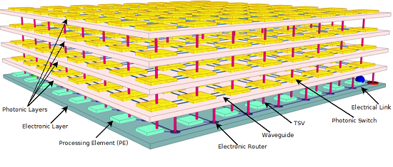
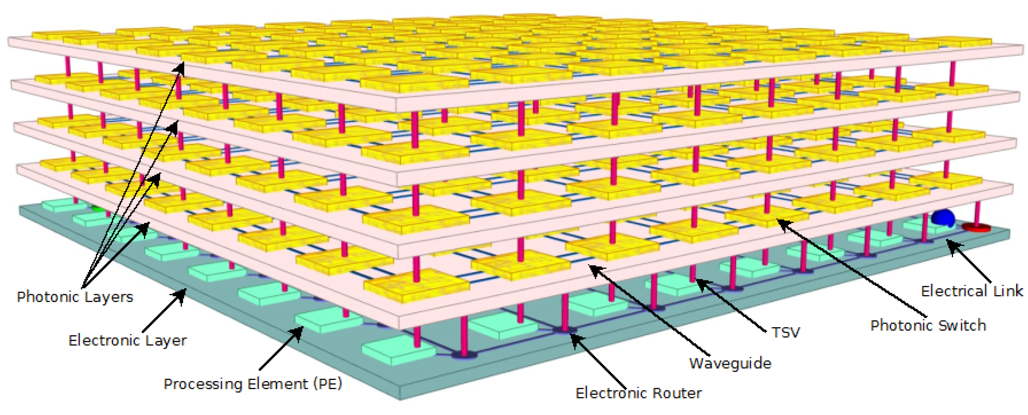
2. System Architecture

The PHENIC-II system organization is shown in Figure 2. The system consists of one Electronic Control Network (ECN) and one or more Photonic Communication Networks (PCN). The ECN is used for path reservation and configuration of the optical switches by mainly powering O N / O F F the Microring Resonators (MRs), while the PCN is based on silicon broadband photonic switches interconnected by waveguides.
Each Processing Element (PE) is connected to a local electrical router and to the corresponding gateway (Figure 3) in the PCN. Messages generated by the PEs are separated into control signals and payload signals. Control signals are routed in the ECN and used for path configuration and routing. The payload data are converted to the optical format and transmitted on the PCN. In the next subsections, we describe in a fair amount of detail the main photonic building blocks, photonic router and the optical path-configuration and routing algorithm.

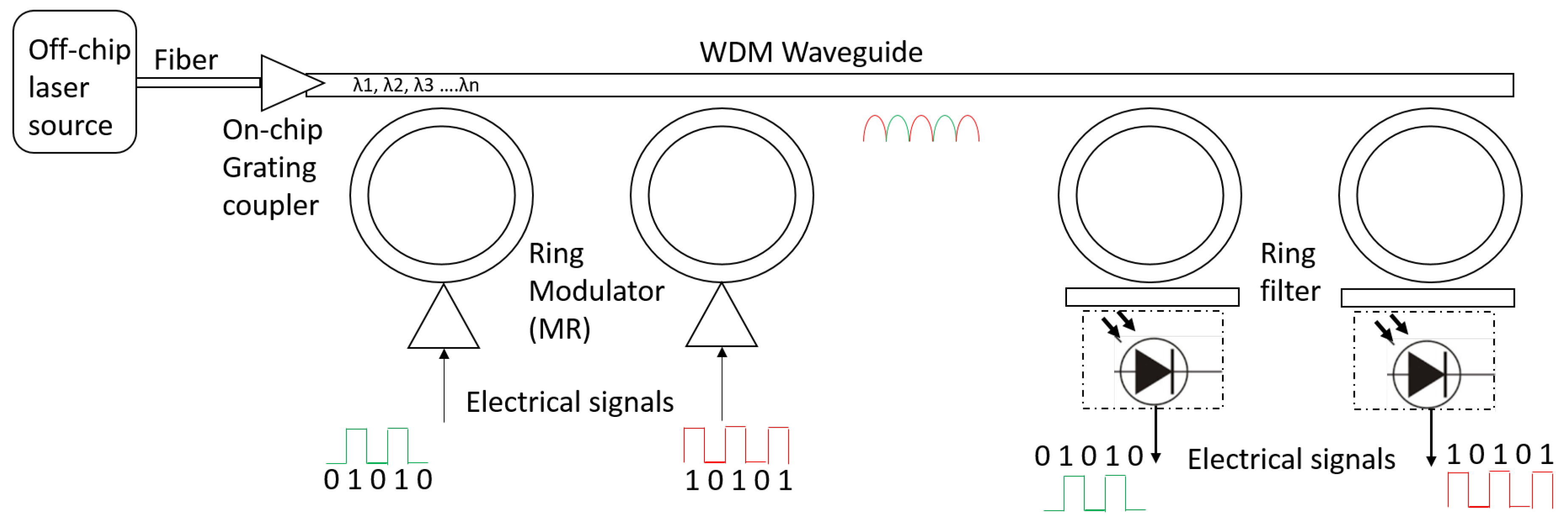
2.1. Photonic Building Blocks

Laser source: Since there is no available high-speed, electrically-driven, on-chip monolithic laser light [22], the PHENIC-II system features an off-chip laser source, such as VCSEL (Vertically Cavity Surface Emitting Laser). As indicated in Figure 1, the off-chip laser source provides light to the modulator(s), which transduces electrical information into modulated optical signals. Then, when the lights enter the chip, optical splitters and waveguides route it to the different modulators used for data transmission.
Modulators: Before optical messages are transmitted, the electrical messages from each IP core should be converted to optical form. PHENIC-II implements at each node a Gateway (Figure 3) serving as a photonic network interface and based on silicon optical modulators and SiGe photodetectors. To reduce conversion time, modulators should be small (i.e., the circular shaped 10-μm ring-modulator [23]) and fast. The performance of a typical modulator is dependent on the on-to-off light intensity ratio [22], which depends on the electrical input signal strength. A higher extinction ratio is better and required for fast and accurate signal detection. Works in [22,23] reported that an extinction ratio greater than 10 dB is acceptable and enough to enable proper signal detection without causing communication errors.
Waveguide: The waveguides provide the physical interconnection between all sources and destinations and enable connectivity between all photonic devices in PHENIC systems. The transmitter demultiplexes the light into appropriate wavelength channels and then modulates each of the channels with a digital data stream generated by the electronic component to be interconnected. Finally, photonic signals are routed to various PEs via routers and waveguides. We have to note here that the refractive index [22] of the waveguide material has a big impact on the bandwidth, latency and area of an optical interconnect. A waveguide typically has a width of 0.3 μm [24]. Once the photonic signals are received by the destination node (receiver), the signals must be converted back to electrical form. Furthermore, since PHENIC-II simultaneously transmits different wavelengths per bidirectional waveguides, a wave selective filter for each received wavelength is needed at the destination node.
Microring resonator: The main element of a silicon photonic NoC system is the Microring Resonator (MR). MRs are capable of effectively guiding an optical signal by carefully choosing their dimensions and positions along the path. Optical signals couple into ring resonators at specific regularly-spaced wavelengths in the optical spectrum, called resonant modes [25].

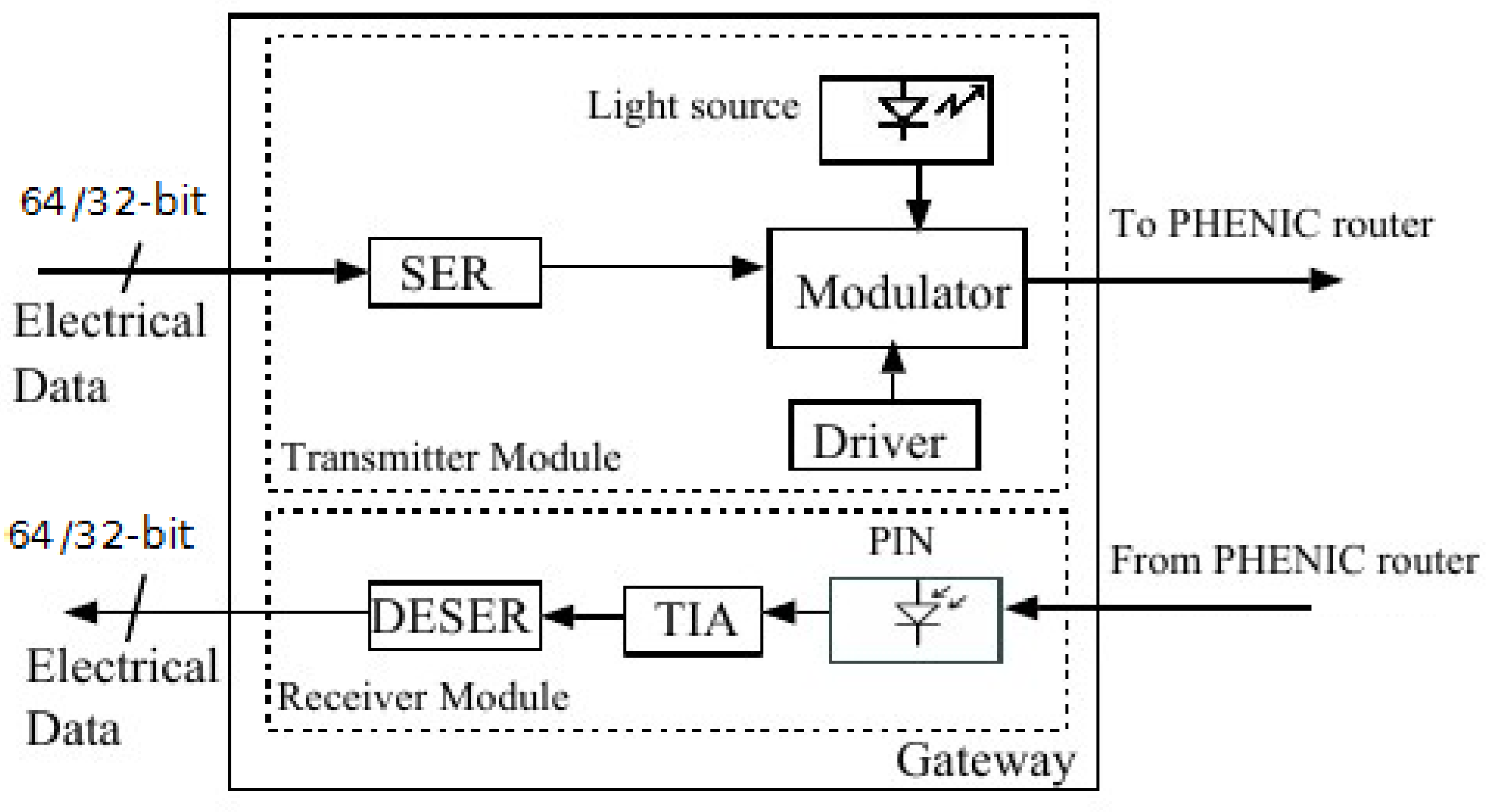
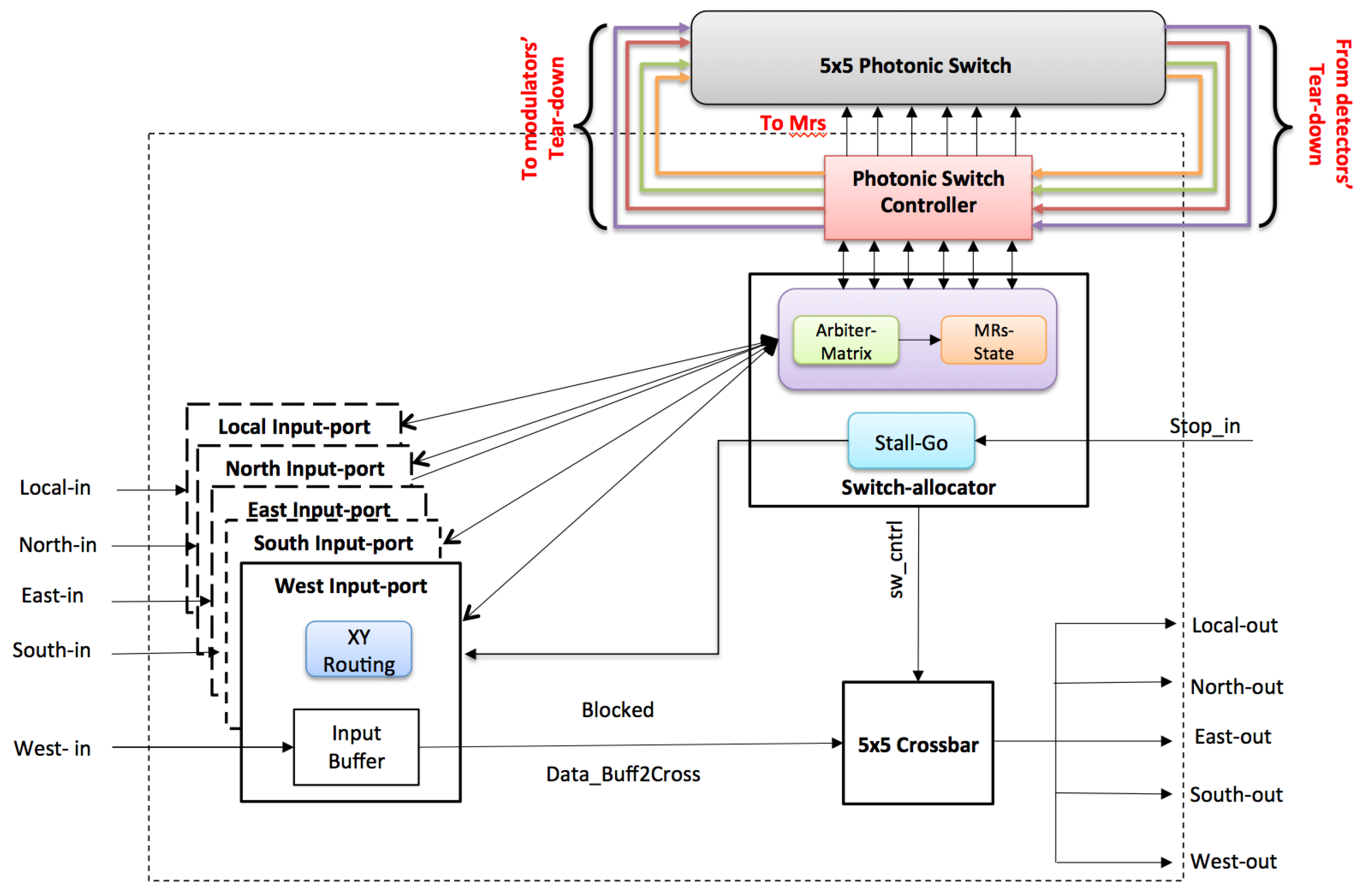
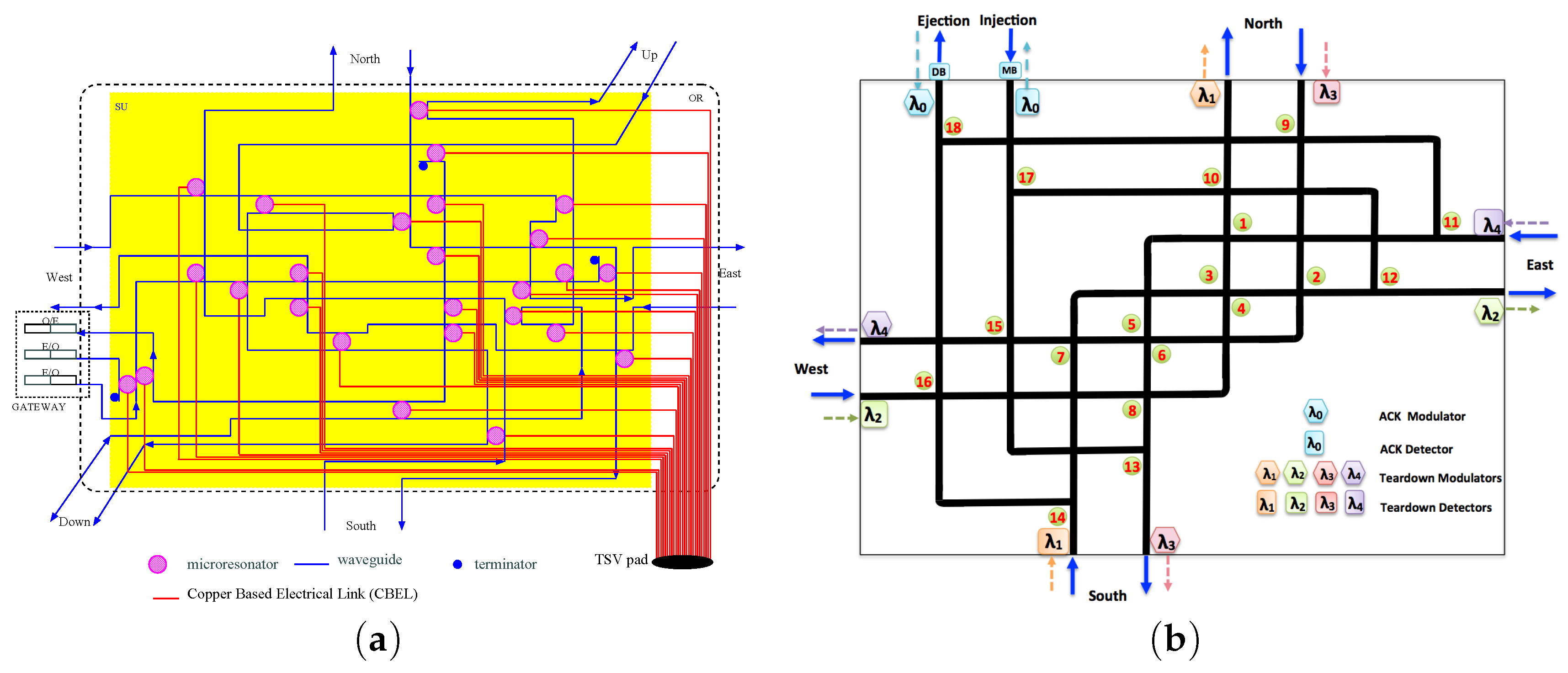
2.2. Photonic Router

The most prevalent photonic network element of the PHENIC-II architecture is the photonic router, which consists of: (1) a non-blocking photonic switch; and (2) an electronic control router.
The system has a mesh-based topology, and control packets are forwarded along the network using a wormhole-like switching policy and then routed according to Dimension-Ordered Routing (DOR-XY) [9,26,27,28,29,30]. The ECN adopts a stall-go mechanism and a matrix-arbiter as a scheduling technique. Figure 4 illustrates the light-weight electronic control router for the 2D system configuration. The control router has three pipeline stages [10,15,31,32]: Buffer Writing (BW), Routing Calculation and Switch Allocation (RC/SA) and Crossbar Traversal (CT).
The non-blocking photonic switches for three-dimensional and two-dimensional configurations are shown in Figure 5a,b, respectively. These switches are based on multiple optical switching elements, and a careful design has been made to reduce waveguide crossings. The MR is used as a simple component to implement the basic 1 × 2 switching element. A given MR element has a resonance wavelength λ m r r e s , which is determined by the material and structure of the microresonator.
When the wavelength λ m r of a given optical signal is equal to the resonance wavelength λ m r r e s of the microresonator, the optical signal makes a turn, as shown in Figure 1. Otherwise, it will pass by the microresonator and will continue in the same direction.

2D Non-Blocking Photonic Switch

The proposed 5 × 5 non-blocking photonic switch is shown in Figure 5b and is based on a 4 × 4 photonic switch presented in [33]. Our proposed switch has extra waveguides, MRs and a gateway used to handle both the data and acknowledgment signals.
As shown in this figure, we used two waveguides (right top side): one for the ejection and one for the injection from the east and the north ports to the gateway. Similarly, two other waveguides were used for the south and the west ports on the bottom left side of the same figure. The given switch can handle the data stream like any other conventional photonic switch, as well as the ACK signals and the resulting regeneration process of the teardown signal at each hop. A hybrid switching policy is used for the data signals. Moreover, since the teardown signals should be checked and regenerated at each hop, it is crucial that their manipulation should be done automatically and without interfering with data signals nor causing a blockage inside the switch. When the teardown is generated at the source network interface, it is first sent to the electronic router. Then, the photonic switch controller releases the corresponding MRs and generates another teardown. At the destination node, the teardown is detected and sent to the photonic switch controller in the corresponding electronic router. In this fashion, the overhead of an additional gateway is omitted.
Table 1 shows the MRs’ dynamic configuration table. As shown in this table, there are 18 MRs used in a non-blocking fashion. As indicated in the table, the photonic switch has four passive directions where there is no need to configure the MRs. These directions are north to west, east to south, south to east and west to north. In order to route the data between any pair of input and output, the electronic controller finds out the required output port and next configures the corresponding MRs. For example, if the packet is coming from the local port and going to the north port, MR Numbers 17 and 10 will be turned ON. We use the first six wavelengths in the optical spectrum starting from 1550 nm, with a wavelength spacing equal to 0.8 nm to maintain a low cross-talk, as reported in [34]. The first wavelength (i.e., 1550 nm) is used to modulate the one-bit signal for the ACK. The next four wavelengths are used for the teardown signals (i.e., from 1550.8 nm to 1553.2 nm); one wavelength for each port, except the local one. The sixth wavelength is used for data transmission (i.e., 1554 nm). Moreover, the five wavelengths used to control the ACK and teardown signals are constant regardless of the network size. Thus, cutting these wavelengths from the available spectrum to be used for control would not degrade the system throughput. These five wavelengths are negligible, especially for the dense wavelength division multiplexing scheme.
In the case where the teardown signals enter the switch, they need to be redirected to the corresponding electronic router. Since these signals are coming from different ports and they are modulated with different wavelengths, detectors capable of switching all four wavelengths are placed in front of the input ports to intercept them, as shown in Figure 5b. According to the control signals, the corresponding MRs will be released. For the ACK handling, when the Path Setup Control Packet (PSCP) reaches the destination, a one-bit optical signal is modulated starting from the output port and travels back to the source.
With this smart hybrid switching mechanism, we take advantage of the low power consumption of the optical link by using optical pulses modulated with the adequate wavelength instead of propagating the acknowledgment signals in the ECN. Second, we take advantage of the WDM proprieties by separating the acknowledgment packets and the data signals and let them coexist in the same medium without interfering with each other. This is in contrast to the electronic domain, where these acknowledgment packets travel for several hops, consequently preventing the waiting cores from sending their PSCP packets.
It is important to mention that by using such a scheme to handle ACK and teardown signals, no additional insertion loss will be added. In fact, since the teardown signal is generated at each hop, the incurred insertion loss is much lower than the worst case insertion loss. For the ACK signal, the insertion loss is the same as the corresponding data signal loss.

2.3. Contention-Aware Path Configuration Algorithm

The pseudocode of the proposed path configuration algorithm is shown in Algorithm 1.
As illustrated in Lines 1–10, the PSCP requests need resources, and depending on their availability, this is granted and allowed to move forward. According to the routing decision, the corresponding MRs are turned ON. If the required resources are not available, the PSCP is converted into a Path_blocked packet. When this latter arrives at a node, the previously reserved resources are released (Lines 11–15). If the PSCP arrives successfully at the destination, the destination’s Network Interface (NI) modulates a one-bit signal to travel back to the source node (Lines 16–20). Upon the arrival of the ACK, the source node modulates the data through data modulators in the gateway (Lines 21–25). At the end of the transmission, the source node sends back the teardown signal.
As shown in Lines 26–31, when a teardown signal arrives at the electronic router from the upper photonic switch, the input port can be decoded (e.g., if the teardown arrives with Wavelength 5 , this means that it is coming from the south input-port). After decoding the input port and according to the destination address encoded, the algorithm finds the output port. According to this port, a new teardown signal is generated for the next hop by modulating the adequate wavelength (e.g., if the output port is north, the teardown will be modulated with Wavelength 1 and will be received by the detector of Wavelength 1 in the south input port of the downstream node. This process is repeated until the teardown reaches its destination.
In conventional path-setup algorithms, the ACK and teardown packets are transmitted in the electronic network and have to go through all of the buffering, routing computation and arbitration stages. With the proposed algorithm, they are carried out via the photonic layer. As a consequence, the End-To-End latency (ETE) can be significantly reduced in addition to the dynamic energy saving that can be achieved. Furthermore, by moving half of the network’s traffic to the photonic layer, the buffer size is reduced to half, leading to less energy overhead in the electronic layer. Nevertheless, with half of the buffer size, we can obtain better bandwidth and less latency.
Photonics 03 00015 i001

3. Evaluation

3.1. Evaluation Methodology

We simulate our proposed PHENIC-II system using a modified version of PhoenixSim, which is a physical-layer simulator developed in the OMNeT++ simulation environment [25]. The used simulator incorporates detailed physical models of basic photonic building blocks, such as waveguides, modulators, photodetectors and switches. Electronic energy performance is based on the ORION simulator [35]. We evaluate the throughput performance and energy consumption for 64- and 256-core systems.
We compare the obtained results with the baseline mesh-based PHNEIC system [1,2] and three conventional hybrid-PNoC architectures [17,18,25]. We chose these three networks for their different behaviors. In fact, the first one has a blocking switch, and the second one is considered as non-blocking, since it uses a crossbar. The third system, which we compared, is a torus-based system having the capability of setting the path with less hop counts by taking advantage of the connections between the edges. We used random and bit reverse traffic patterns. Random traffic is a communication pattern where the destinations are randomly and uniformly selected each time a new communication occurs. In bit reverse, each node sends messages to the complement node of its ID, thus resulting in very long communications to observe the scalability of the proposed system.
Furthermore, we evaluate the performance of the proposed system using two realistic workloads: the Cooley-Tukey FFT algorithm [36] and the data flow/streaming execution model [25]. More details will be given about these two benchmarks in Section 3.3. Table 2 and Table 3 show the energy parameters’ configuration for the photonic communication network.

3.2. Evaluation under Synthetic Workloads

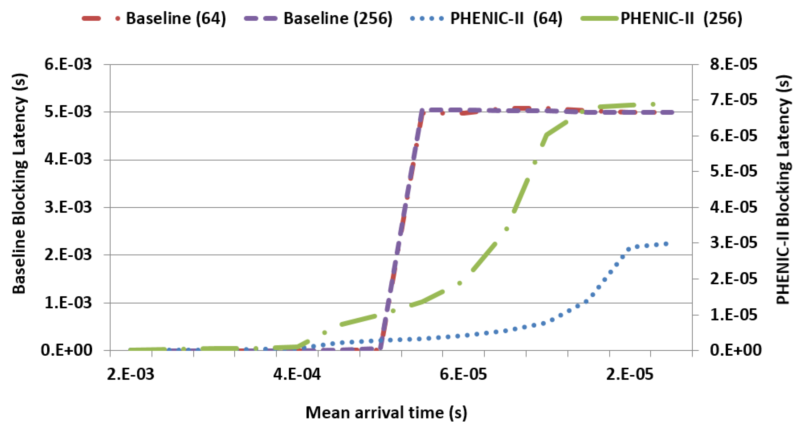
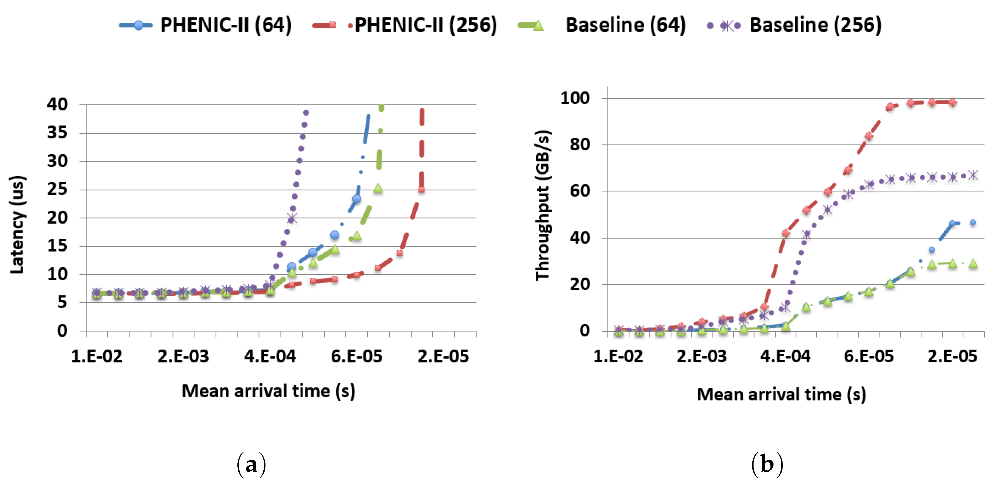
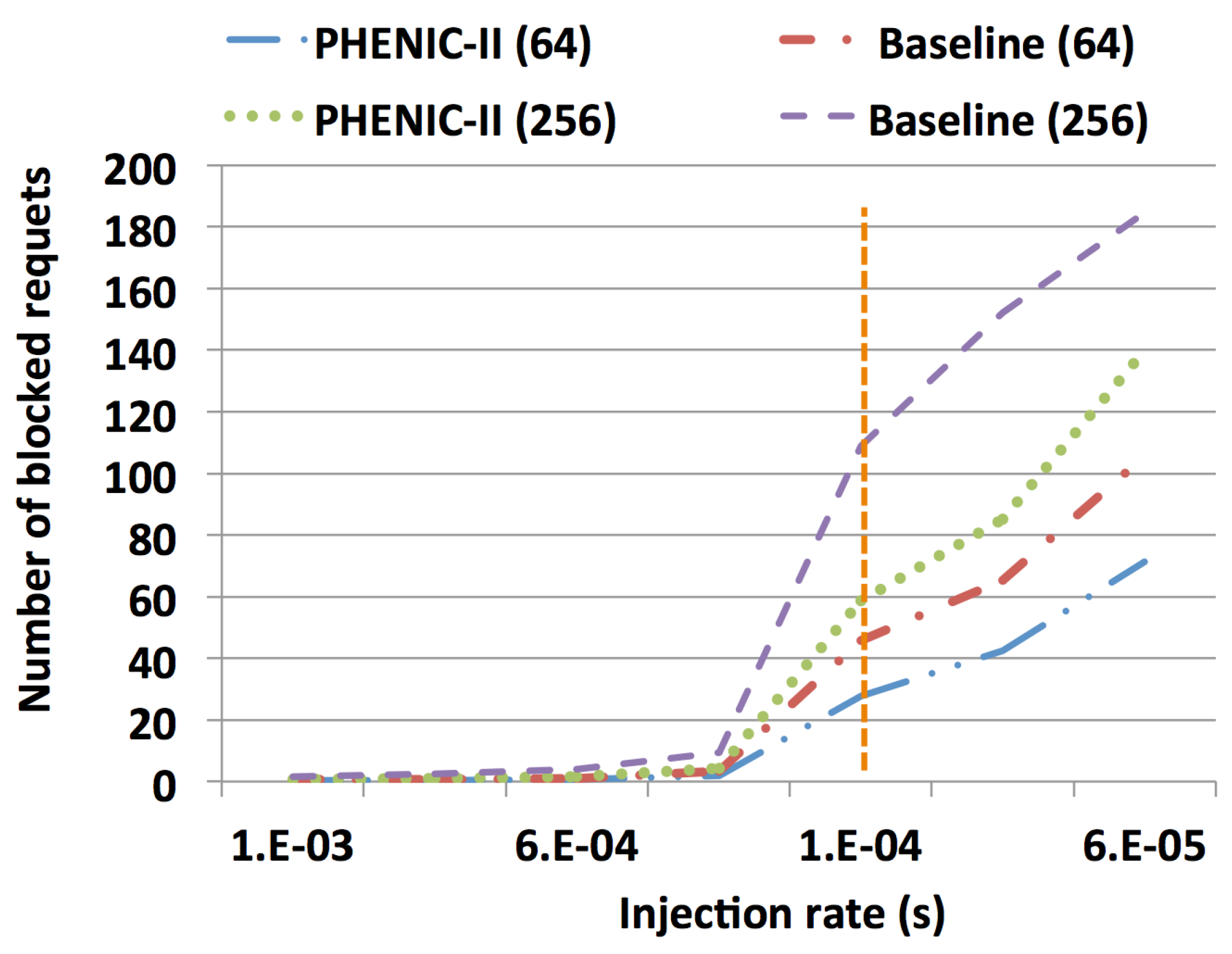
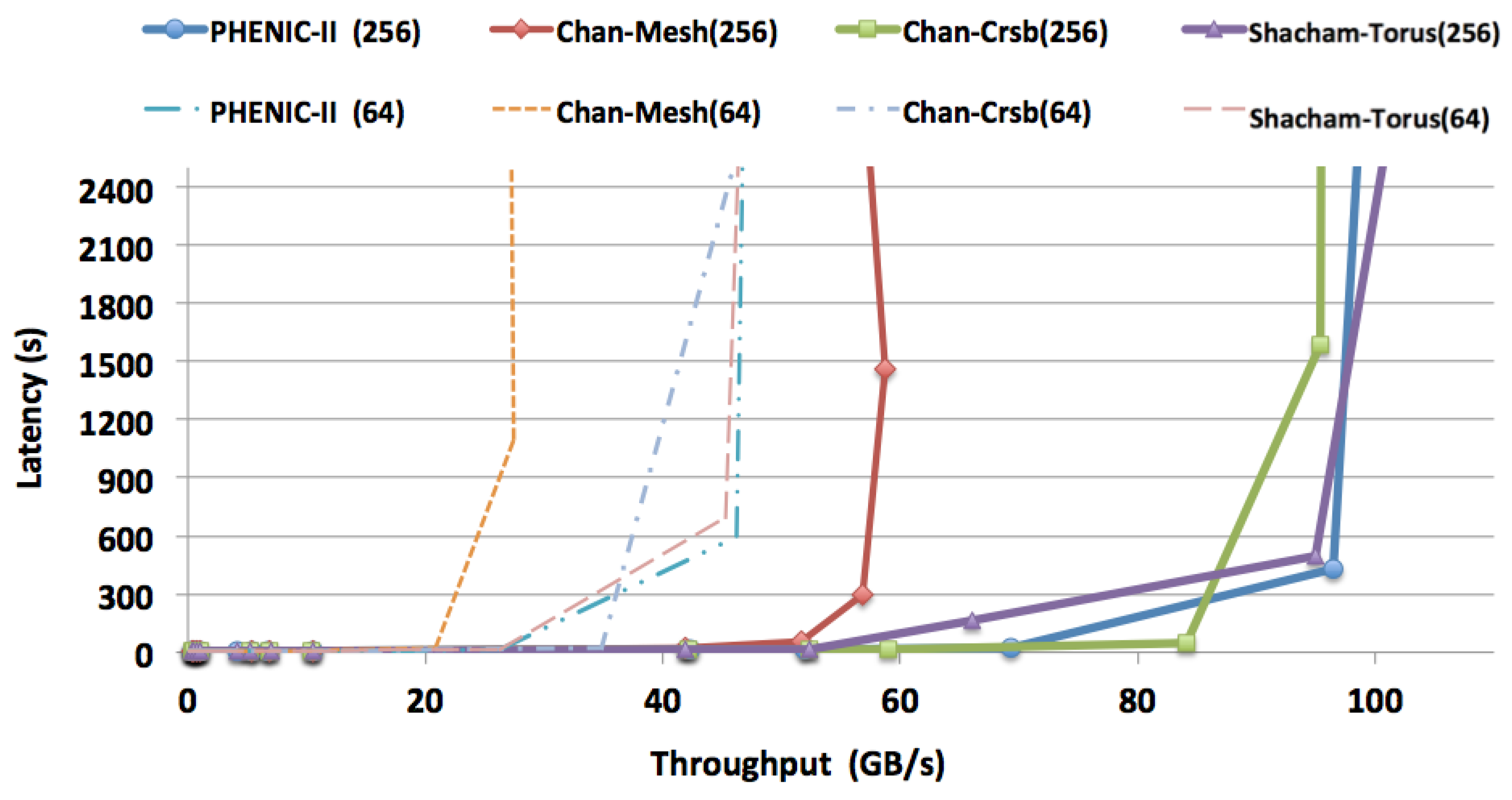
3.2.1. Latency and Throughput Evaluation

Figure 6a,b shows the average latency and the achieved throughput, respectively, for PHENIC-II and baseline systems for 256- and 64-core systems. We can see that for zero-load latency, all networks behave in the same way. Near saturation, PHENIC-II shows more flexibility and scalability in 256 cores when compared to the baseline. For the 64-core system, the baseline slightly outperforms the PHENIC-II system regarding latency. This can be explained by the use of optical-to-electronic conversion of the teardown, which affects the overall latency for small networks. For the achieved throughput, Figure 6b clearly shows the gap between the two networks, where for the 64-core system the throughput is increased by 24%, and for 256 cores, it is increased by 51%. This good performance can be explained by Figure 7, where the average blocking latency is measured. The blocking latency is defined as the average of the blocking time added to the overall latency due to the unavailability of the resources. From Figure 7, we can see two majors improvements. The first one is the gap between the two systems for 64 and 256 cores, reaching 200%. The second improvement is the scalability of the proposed system. This can be seen in Figure 7, where the PHENIC-II blocking latency curve is flatter than the baseline one, and the network can still accept other communications, even when the injection rate is high; in contrast with the baseline system where at a certain injection rate, the network saturates.

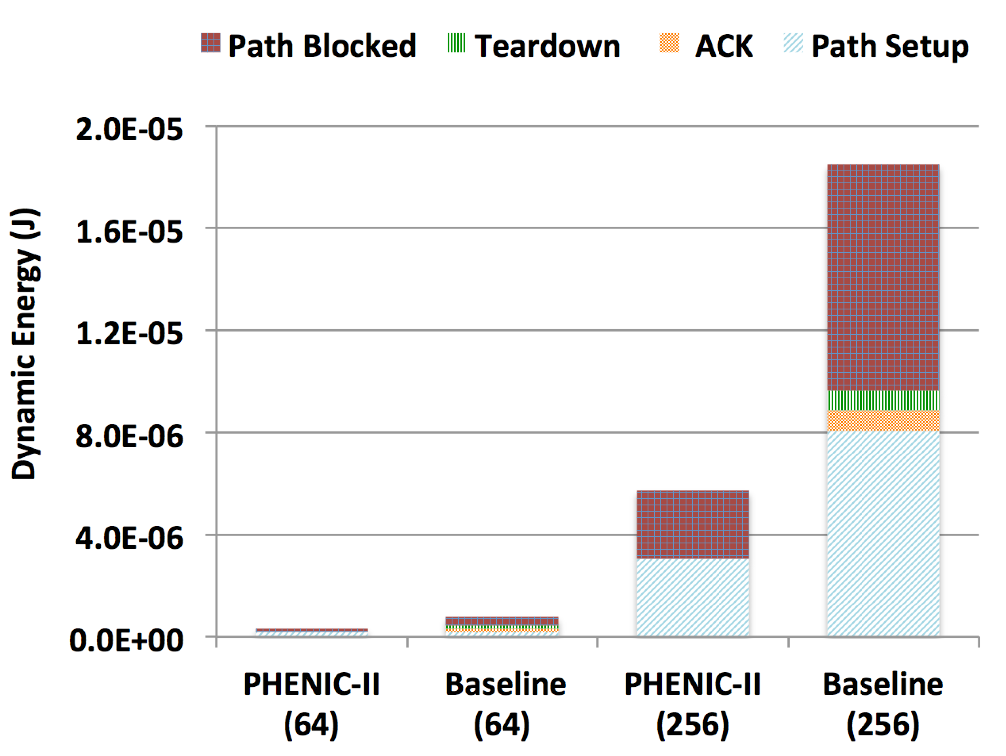
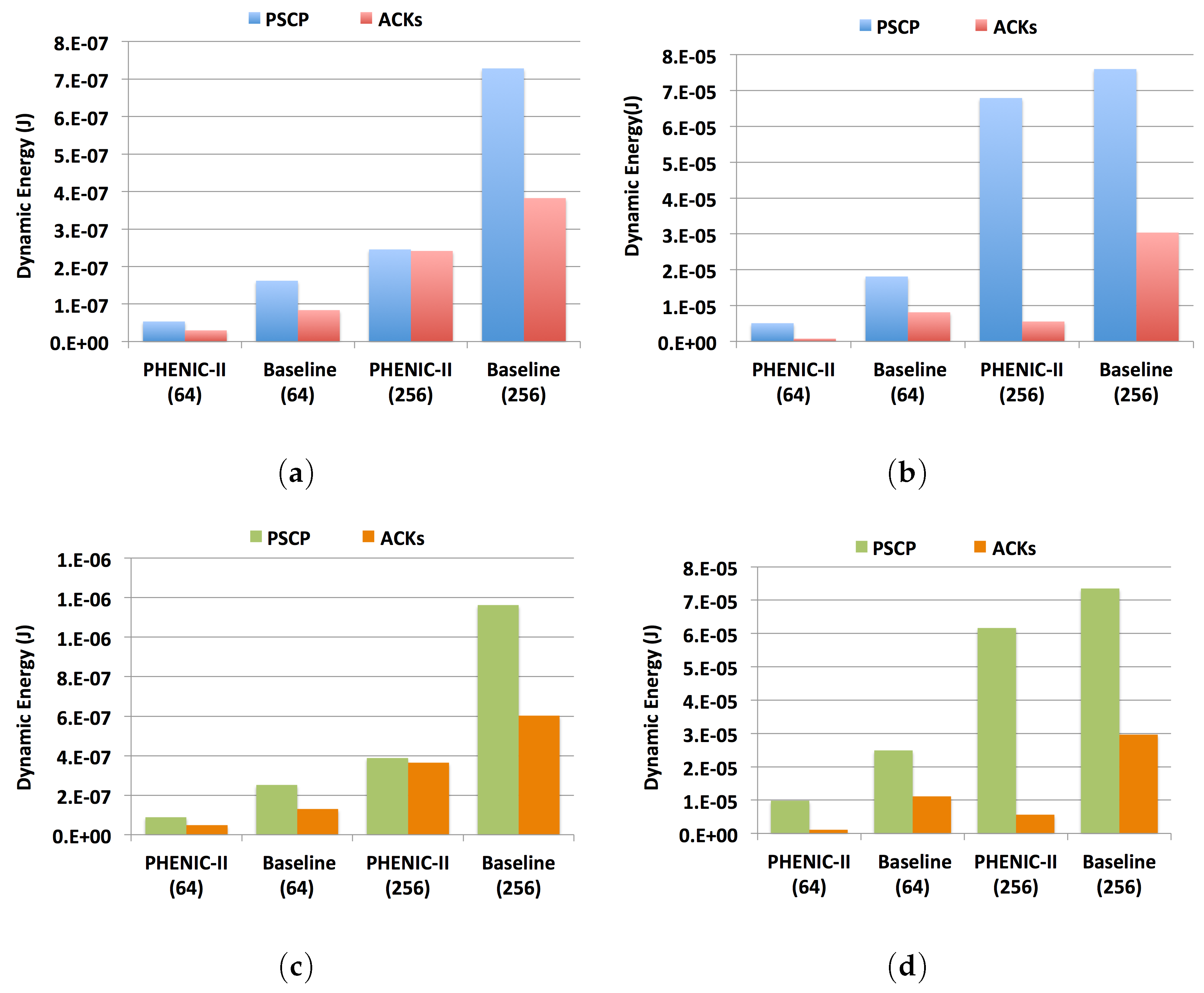
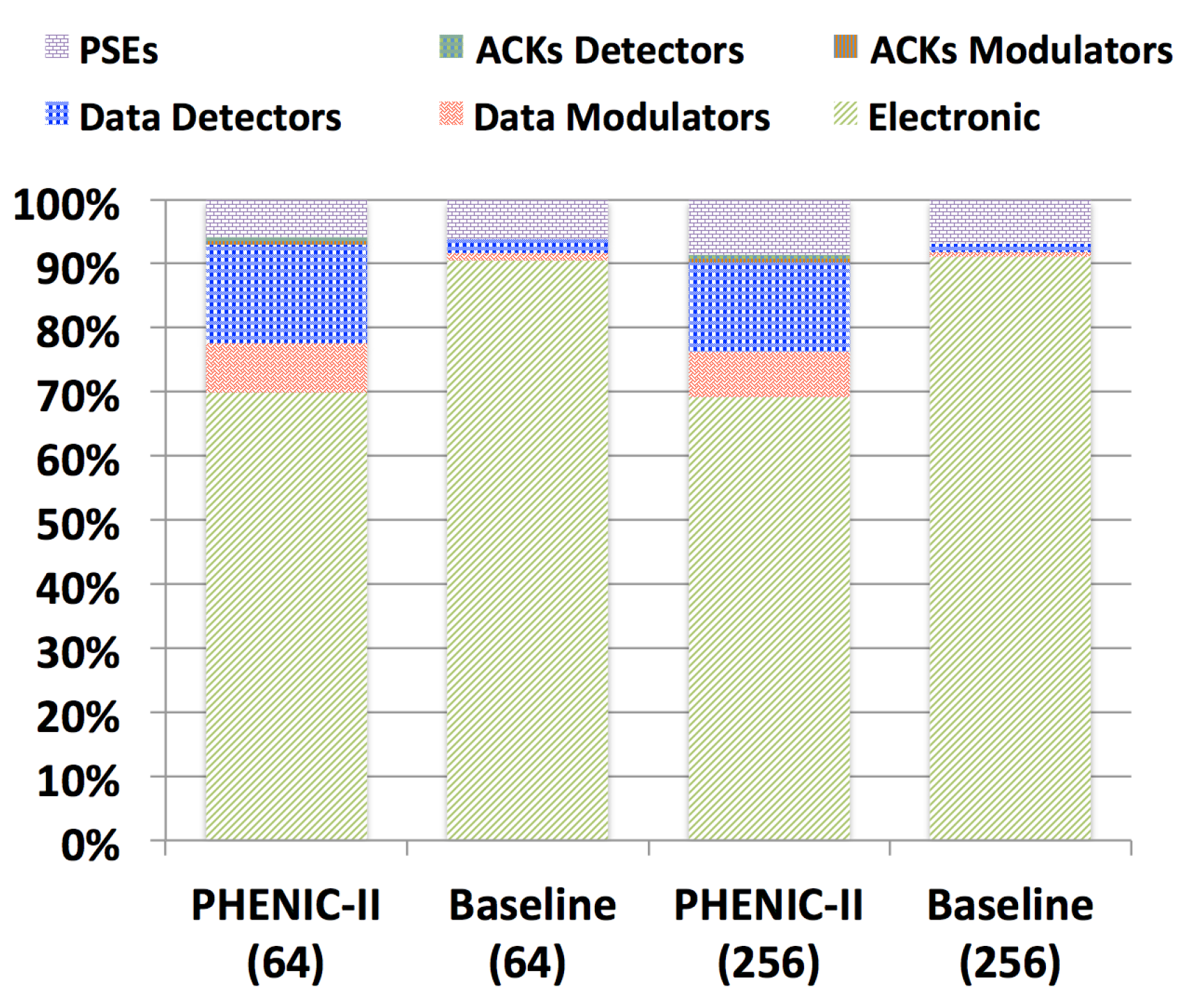
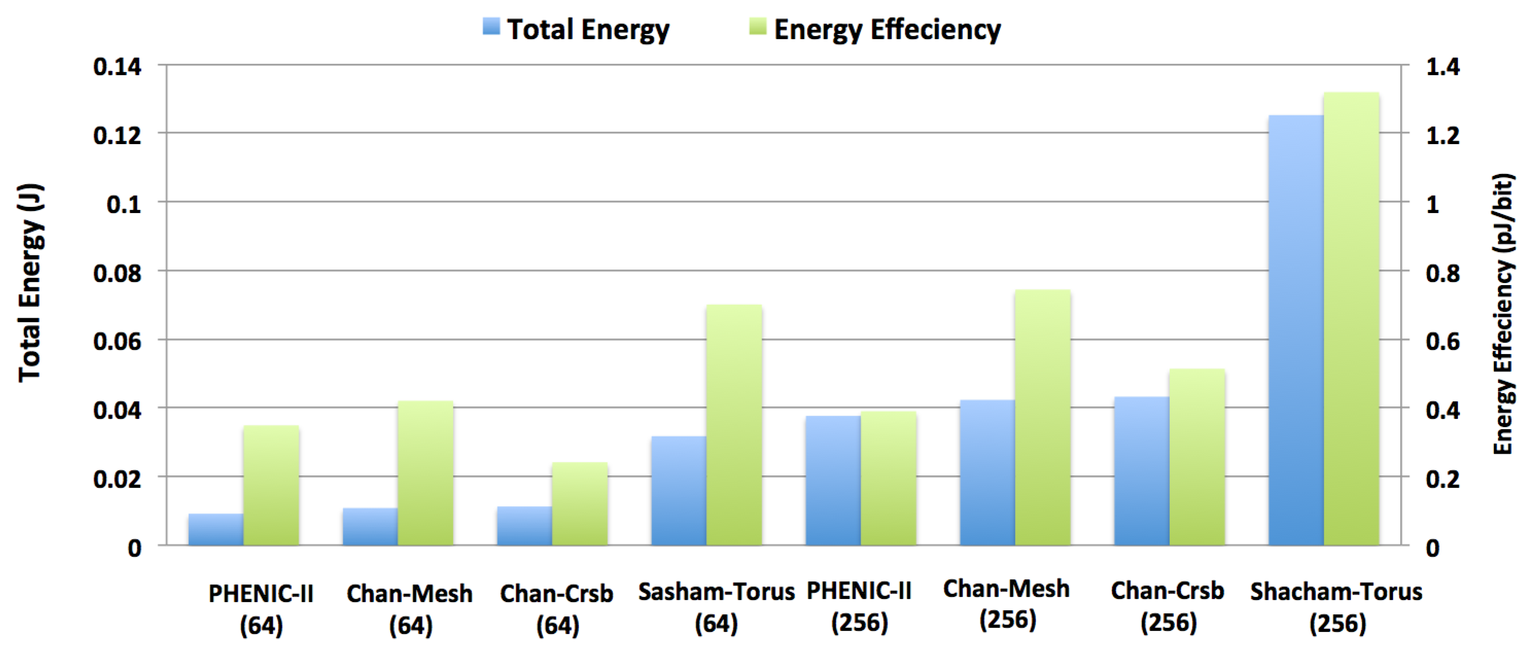
3.2.2. Energy Evaluation

We evaluate the energy overhead of the PSCP, which is given by Equation (1), where P S S u c c is the dynamic energy in the ECN dissipated by the successful PSCPs reaching their destinations and P S F a i l e d is the dynamic energy consumed by the PSCPs, which resulted in Path_blocked packets. We also evaluate the ACK energy overhead, which is defined as: (1) the energy dissipated by the ACK and teardown packets for the baseline system; and (2) the sum of the dynamic energy of the modulators and detectors used for the optical ACK and teardown signals in the PHENIC-II system. These two definitions are represented by Equations (2) and (3), respectively.
P S C P E n e r g y = P S C P S u c c + P S C P F a i l e d
E A C K s E n e r g y = A c k P a c k e t + T e a r d o w n P a c k e t
O A C K s E n e r g y = A C K s M o d u l a t o r s + A C K s D e t e c t o r s
Figure 8a,c shows the PSCP and ACK dynamic energy overhead for half-load traffic under random and bit reverse benchmarks. As can be seen in these two figures, the energy overhead of the PSCP considerably decreases by almost 66% for both 256- and 64-core systems. The same enhancement can also be seen for the ACKs energy, which is also considerably reduced by 36% in the 256-core and 64% in the 64-core systems. This decrease in the PSCP energy proves the benefit of the proposed system where most of the PSCP requests succeed at reaching their destinations on the first try without resulting in a path being blocked. This is not the case for the baseline system where the PSCP energy, also high, exceeds largely the ACKs’ energy.
Figure 8b,d represents the energy overhead when the system is fully loaded (i.e., near the saturation point) for random and bit reverse traffic, respectively. We can notice that the decrease in the PSCP energy is only about 10% in the 256-core system, but still considerable for the 64-core system, which is about 60%. This is because when many PSCPs are injected into large networks, the blocking can be avoided to a certain limit; but, due to the photonic resources limitation, some of the requests become blocked. This problem is mostly related to the structure of the switch and can be avoided by using high-radix switches, also related to the used routing algorithm. For the acknowledgment’s energy, it is clear that the optical handling of the teardown and ACK adopted in PHENIC-II is more energy efficient for the two benchmarks and the two network sizes.
This can be clearly observed in Figure 9, where for the 256-core system, the energy gain reaches 20%. Moreover, the energy efficiency is close to the baseline 64-core system. In Figure 10, the energy breakdown is shown for both systems. Compared to the baseline system where the electronic energy is reaching 90% of the total energy, PHENIC-II shows more balanced energy repartition between the photonic and electronic networks. This is despite the fact that the electronic power is still high with 70% of the total system energy. When we dig more into the energy evaluation, we find the explanation of this energy-efficient scheme. Figure 11 shows the buffering dynamic energy comparison results. From this figure, we can see first how the dynamic energy of the PSCP is decreased by 50% when compared to the baseline system. We can also see the significant decrease in the Path_blocked dynamic energy, which is a direct consequence of the considerable decrease of the PSCP dynamic energy. This behavior is more noticeable for 256-core systems.
Our final evaluation in this subsection is shown in Figure 12, which shows the number of blocked requests having reached more than half of the network diameter (i.e., PSCPs, which failed to reach their destinations after traveling more than half of their path). We can see that for low injection rates, the two networks behave the same way. While when the injection rate increases, we can see that for the baseline system, for both 256 cores and 64 cores, the number of the blocked requests largely exceeds PHENIC-II.
Near the saturation point (represented by a vertical dashed line in Figure 12), the number of blocked requests for PHENIC-II 256 cores decreases by 42% and by 35% for the 64-core system. Furthermore, the curve for the baseline system is more aggressive, in contrast with PHENIC-II. In this figure, we are only showing the most energy-costly (i.e., packet blocked) portion, since if a PSCP is traveling for more than half the network and after that it is canceled, this incurs high and wasted energy dissipation (i.e., buffering, switching, crossbar traversal).

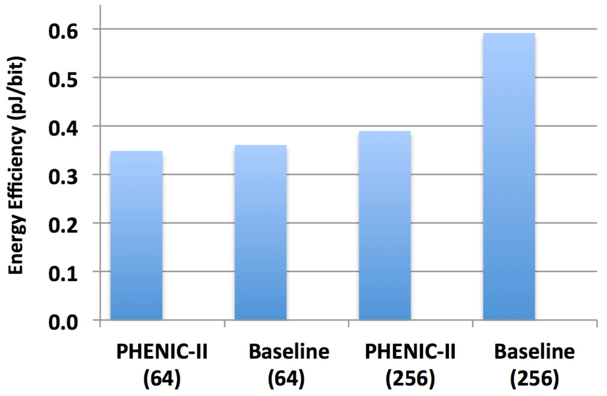
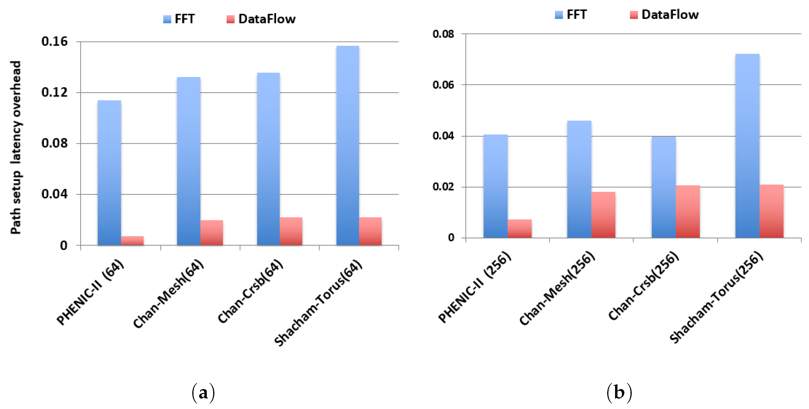
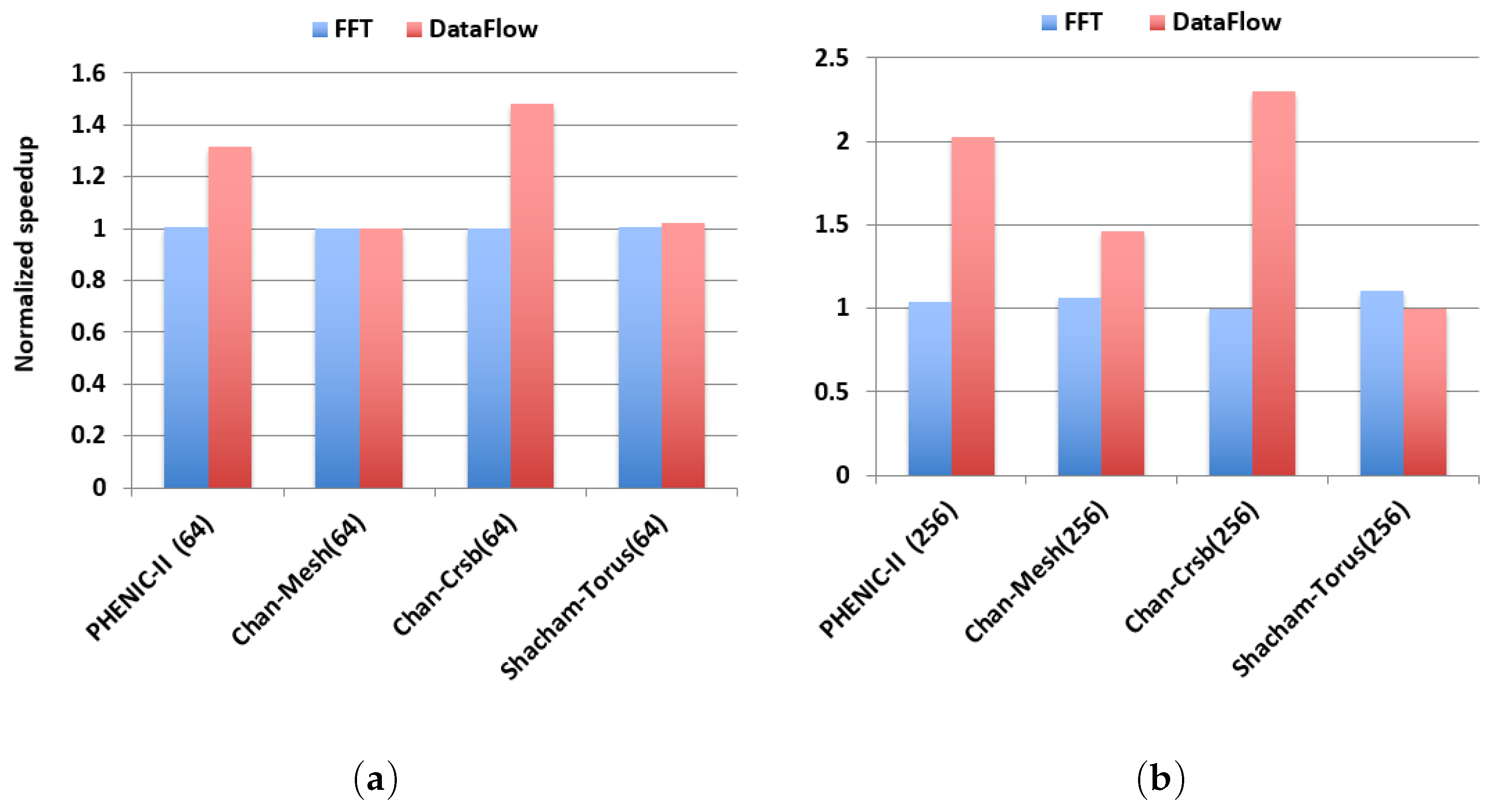
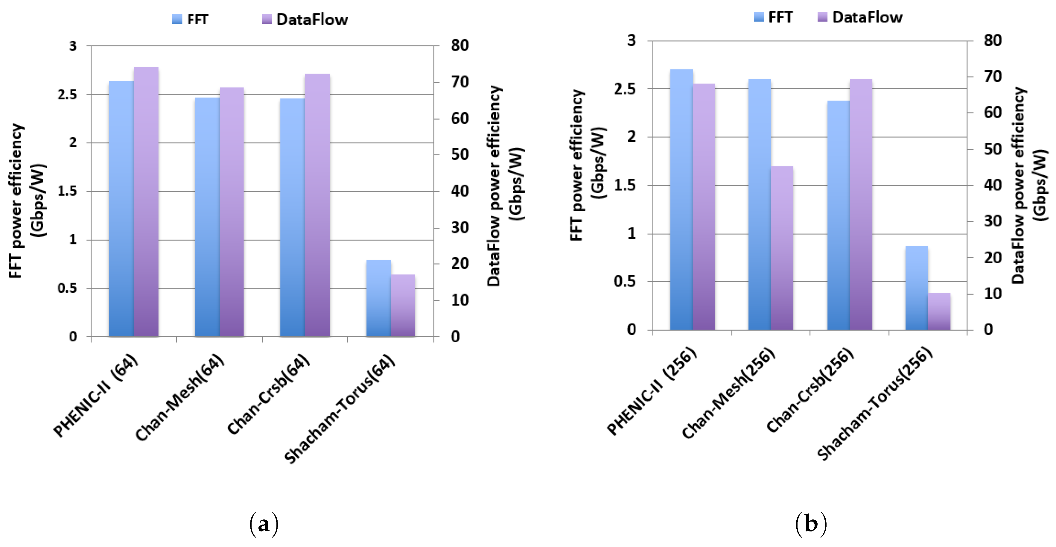
3.2.3. Performance and Energy Efficiency Comparison Results

We start this subsection by comparing the performance of the PHENIC-II system to the three previously-mentioned systems. Figure 13 shows the average latency vs. the total achieved throughput for 64- and 256-core systems. We can see that regarding saturation, the blocking mesh and the crossbar behaves in the same way. After a certain injection rate, the network saturates. Moreover, the crossbar-based system largely outperforms the blocking mesh. The PHENIC-II and torus systems show different behaviors. In fact, for these two networks, the saturation curve is less aggressive, and they prove the capability of handling more communications and more scalability than the two other networks. While the torus system has the capability of setting the path with less hop counts, we can see that the PHENIC-II system can achieve the same performance without the need for extra wiring to connect the edges. This behavior is observed for both 64- and 256-core systems.
Figure 14 shows the total energy and the energy efficiency comparison results of the four networks for 64- and 256-core systems. For the 256-core configuration, the proposed system outperforms all other systems; especially, we can see an improvement regarding energy efficiency reaching 26% and 48% when compared to the crossbar-based (non-blocking) and the mesh-based (blocking), respectively. When compared to the torus-based architecture, PHENIC-II improves the energy efficiency by up 70%. The torus-based architecture offers high throughput thanks to the connection between edges, leading to short communications. On the other hand, it comes at a high energy cost. This can be explained by the fact that the additional input ports, required for the edge connections established in the torus-based system, incur an increased area and, consequently, an energy overhead.
From these results, we can see that PHENIC-II outperforms systems whether having non-blocking or blocking switches. Besides, it provides much better energy efficiency than the torus-based, which can offer the same throughput as the proposed system. We can conclude that the obtained improvement by PHENIC-II is the result of the association of three main factors together: (1) the non-blocking switch supporting optical acknowledgment signals; (2) the light-weight router with reduced buffer size; (3) and the path setup algorithm to adopt hybrid switching inside the photonic switch.

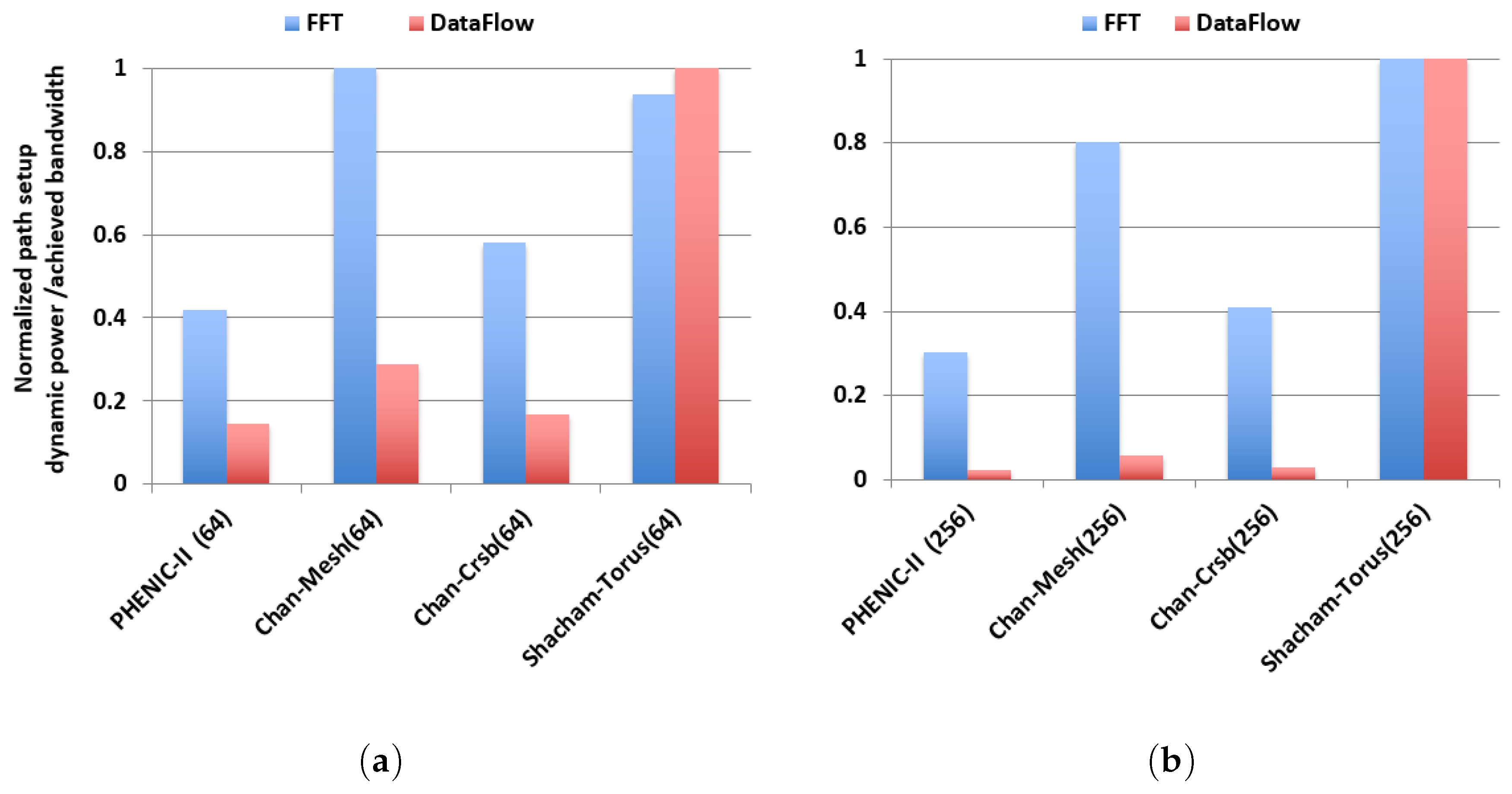
3.3. Evaluation under Realistic Workloads

In this subsection, we evaluate the performance of the proposed system using two realistic workloads: the Cooley–Tukey FFT algorithm [36] and the data flow/streaming execution model [25]. The traffic pattern generated by the FFT algorithm is modeled according to [37]. In this traffic, each core starts reading from the memory. Then, it processes k = m / M sample elements, where m is the size of the array of input samples and M is the number of cores. After this phase, the algorithm proceeds with a sequence of log M iterations. At each iteration, the processors exchange data according to a butterfly scheme, resulting in long-distance communications. Finally, a write to the memory step is executed where the cores store the exchanged data. To get the characteristics of the computation and communication steps, the Pentium-M core was used as a reference according to the work in [37,38]. The Pentium-M takes 39.32 ms to compute the FFT on 256k samples and 2.18 ms for the communication stage.
For the data flow execution model [25], each core computes some part of the total computation (i.e., piece of data), passes it on to other core and repeats the same computation for the next piece of data that arrives. In this fashion, a large dataset is broken into small chunks and processed in parallel through all of the cores in the network. In this application, only cores from the edges read and write to the memory, and the data are exchanged on a hop-by-hop basis, resulting in short-distance communications. With these two applications, we can observe the effects of short- and long-distance communications on the proposed system performance.
Figure 15a,b shows the average path setup latency overhead comparison results for 64-core and 256-core systems, respectively. As shown in Equation (4), the path setup overhead is defined as the ratio between the average time needed to set the path and the average time required for the transmission. The time necessary for setting the path includes the time to send the PSCP in addition to the time resulting from blocked packets and the ACK. In other words, the network efficiency is higher when the average path setup overhead is low.
P S L O v e r h e a d = T P a t h R e q u e s t + T P a t h B l o c k e d + T A C K T t r a n s m i s s i o n
Since the exchange of data is done in a hop-by-hop basis in the data flow application, we can see a low path setup overhead for all networks. However, PHENIC-II achieves the lowest latency overhead when compared to other systems, which can reach 50% when compared to the Torus architecture. When it comes to the FFT application, we can see the impact of long communications. In fact, the path setup latency overhead increases considerably for all networks and both sizes.
Nevertheless, the PHENIC-II system achieves up to 30% and 50% improvement when compared to the Torus architecture for 64 and 256 cores, respectively. When compared to the blocking and the crossbar architectures, an improvement of 10% and 5% can be observed, respectively. When evaluating the speedup, the data flow application with its short communication affects the performance of the studied systems. In fact, the Torus architecture can no longer take advantage of its capability of using the edges. Therefore, it has the lowest speedup among all networks, as shown in Figure 16a,b. For the PHENIC-II system, it outperforms the Torus and the blocking networks when running the data flow application for both network sizes. However, it is outperformed by the crossbar system by 11%. This is due to the one-hop communication characteristic of the data flow workload, which affects the process of modulating and detecting the teardown in the proposed system for just one hop. When it comes to the FFT, the Torus architecture slightly outperforms all other networks, taking advantage of the communication between the edges.
We also compared our proposed system to other networks regarding power efficiency. First, we evaluate the dynamic power required to set the path. Figure 17a,b shows the normalized dynamic power consumption per achieved bandwidth. We could see that using the optical signaling for path configuration in the PHENIC-II system reduces the dynamic power consumption by up to 20% and 60% when compared to the blocking and the crossbar architectures, respectively. We also noticed that the Torus system is largely penalized regarding power because of its additional ports to connect the edges. Moreover, the benefits of using optical signaling in the path setup are more noticeable regarding energy for long-distance communications (i.e., FFT traffic pattern) rather than shorter ones (i.e., data flow traffic pattern).
Finally, we present the results of the power efficiency. It is calculated as the ratio of the achieved bandwidth in Gbps to the total power consumption in watts (static and dynamic). The results are shown in Figure 18a,b. We can see that the Torus system is always penalized regarding power efficiency. Furthermore, in the FTT benchmark for 256 cores, the PHENIC-II system outperforms the blocking and the crossbar architectures by 5% and 14%, respectively. For the data flow, PHENIC-II outperforms the blocking architecture by 51% while observing the same behavior as the crossbar architecture. It is important to mention that since the two applications have intensive access to the memory, in the PHENIC-II system, we also use the optical signaling for any acknowledgment between the memories banks and the cores (e.g., request for read/write); thus, achieving more network efficiency and contributing to lower power consumption and lower path setup overhead.

4. Related Work

Many works have been conducted so far to solve the various challenges in PNoC designs in general. Before we develop the different proposed hybrid architectures and how researchers tried to solve the previously=mentioned limitations of hybrid-based schemes, let us first review the most well-known fully-optical-based architecture.
Vantrease et al. proposed a 3D stacked 256-core fully-optical architecture named Corona to completely remove all electrical interconnects, replacing them by an optical crossbar and token [39]. In a later work [40], they presented channel-based and slot-based protocols for their arbitration mechanism in addition to a flow-control for fully-optical interconnects. Gu et al. proposed a fat-tree-based fully-optical network (FNOC) [41]. They omit the electronic control layer by using an Optical Turn-Around Router (OTAR), which carries both payload data and network control data on the same optical network. Joshi et al. [42] proposed an all-optical network based on the Clos topology. While it is an interesting work and less complex than the full crossbar topology in the Corona architecture, the topology still requires complex point-to-point photonic links and high-radix photonic routers to ensure the connections between different cores. Li et al. proposed LumiNOC [43], which divides the network into sub-nets for better efficiency. It shows better bandwidth per watt in addition to better photonic resource utilization with fewer waveguides and fewer rings when compared to similar fully-photonic architectures. Kao et al. proposed BLOCON [44], which is a bufferless Clos-based PNoC system. In this work, the authors eliminated the multi-stage buffering in the switch modules found in [42]. The results proved the outperformance and power efficiency of the proposed system when compared to [42]. Pasricha et al. [45] proposed using an optical ring waveguide with bus protocol standards to replace global pipelined electrical interconnects. Beausoleil et al. [46] proposed a crossbar-based ONoC , where 64 wavelengths are multiplexed over 270 waveguides. Two hundred fifty six waveguides are allocated for control and data, and 14 waveguides are for broadcast and arbitration. Zhang et al. [47] introduced a multilayer nanophotonic interconnection named MPNOC, which uses multiple layers to create a crossbar with no optical waveguide crossover. A recent work proposed by Randy et al. [48] also uses a multi-layer photonic interconnect with a microring resonator for the intra-layer communication rather than TSVs (Through Silicon Vias) , as used in [47]. Kirman et al. [49] proposed a fully-optical ONoC using a wavelength-based oblivious routing, where each node has physical connectivity to all other nodes via static paths. For the wavelength allocation between the nodes, they use a wavelength-reuse algorithm proposed by Aggrwal et al. [50]. Chen et al. [51] proposed a fully-optical NoC, which uses a two wavelength assignment methods, called Source-based Wavelength assignment (SW) and Destination-based Wavelength assignment (DW). Some other works focused on how to reduce the crossbar complexity in fully-optical architectures. Pan et al. proposed Flexishare [52], which is a flexible crossbar topology that allows channel provisioning according to the average traffic load and a distributed token stream arbitration, which provides multiple tokens for a given channel.
Many research groups proposed hybrid optical-electronic architectures. These works can be classified into two categories: the first one is a circuit-switched based architecture, where the electronic network is used for control, and the data transmission is performed in the optical layer. The second category is cluster-based, where the electronic and the optical networks are used for local and global communications, respectively.
Hendry et al. [53] proposed a circuit-switched memory access in photonic interconnection networks. This work represents a typical hybrid-PNoC, where all path setup steps are generated and executed in the ECN. Chan et al. [54] proposed a circuit switched electro-optical NoC for core-to-memory connections with the addition of a wavelength-selective spatial routing to increase the path diversity and the throughput. Chan et al. [17] also proposed a circuit switched mesh using a 4 × 4 non-blocking switch augmented with two gateways for ejection/injection from/to the network. An optical crossbar using 56 waveguides was also used in this work. Sacham et al. [21] proposed a torus hybrid-PNoC based on a blocking 4 × 4 optical switch with an extra network for the ejection/injection from/to the torus. Petracca et al. [19] proposed a non-blocking torus hybrid-PNoC where the conventional path setup scheme is used. Cisse et al. [5] proposed a hybrid-PNoC torus named HPNoC, which uses predictive switching [55] in the ECN to reduce the setup latency by reducing the pipeline stages of the electrical router. Although the latency is reduced by using such predictive switching, the path setup steps are all generated and transmitted in the ECN. Ye et al. [3] proposed a new protocol, called Quickly Acknowledge and Simultaneously Teardown (QAST), to reduce the control delays during the path setup and teardown processes. QAST uses an optical ACK signal and sends a teardown packet at the beginning of a transmission instead of sending it at the end of the transmission, as in conventional hybrid-PNoCs. Optimizing the teardown to be sent in parallel with the transmission does not solve the problem of the path setup procedure; because the optical transmission of the data is very short and sending the teardown after, or at the same time, does not reduce the latency overhead.
In a recent work proposed by Wang et al. [20], the typical ECN is reduced to one central controller to process all path setup request packets and to set the corresponding optical switch according to a Microring Resonators (MRs) state table. Although this solution reduces the hop count in the ECN, it suffers from the complex centralized router, and the electronic layer cannot be used like a conventional one if we want to use it for small packets (e.g., cache block broadcasting). Another interesting work to solve the path setup problem was proposed by Hendry et al. [56,57], where they completely remove the ECN, and they substitute it by a time division multiplexing arbitration scheme that provides round-robin fairness to set up photonic circuit paths. In this work, instead of fixing the path in the ECN, each communication between any pair of nodes is only allowed to be active during a particular time slot. According to the obtained results, the electronic energy did not decrease. This is because of the buffering required when there is a switching between X and Y directions. Moreover, the path is fixed at the design level. For cluster-based architectures, Pan et al. proposed Firefly [58], which reduces the crossbar complexity by designing smaller optical crossbars connecting selected clusters and implementing electrical interconnect within the cluster. Another recent work was proposed by Tan et al. [59], where a butterfly fat-tree-based hybrid optoelectronic NoC architecture is introduced using the generic wavelength-routed optical router. However, the wavelength assignment used in this approach for routing purposes leads to an inefficient use of the optical spectrum, as we previously explained.
To the best of our knowledge, none of the existing solutions take advantage of circuit-switching benefits by using the entire optical spectrum through WDM for end-to-end communication and combines them with a contention-aware path configuration algorithm.

5. Conclusions and Future Work

In this paper, we proposed an energy-efficient and high-throughput hybrid silicon-photonic network-on-chip architecture (PHENIC-II). The system is based on a smart contention-aware path setup algorithm and an energy-efficient non-blocking optical switch. Simulation results show a considerable improvement regarding performance with up to a 50% increase in throughput. The energy evaluation shows a decrease of 60% for the acknowledgment signals and 10% for the path setup control packet energy. This performance comes from the decline in the blocking latency and the number of blocked requests. When compared to other architectures, the PHENIC-II system shows better energy efficiency, especially for 256-core systems, while maintaining the same throughput. When evaluated under realistic workloads, the system shows better network efficiency and a reduction in dynamic power by up to 50% and 60%, respectively.
As future work, we plan to investigate the reliability issue of the system. The thermal behavior of the chip remains the main problem in photonic networks-on-chip, since most of the photonic devices are wavelength sensitive, and the proper functionality of the rings could be affected. As a result, the reliability issue is the major challenge. In particular, the parameters of the on-chip nanophotonic structure are sensitive to fabrication process variation and run-time thermal variation. Further study about the reliability that arises from this sensitivity will be investigated.

Acknowledgments

This work is partially supported by the University of Aizu Competitive Research Funding (CRF), Ref. P-12-2014-2015. We wish to thank all anonymous reviewers for providing us useful comments and suggestions.

Author Contributions

Achraf Ben Ahmed and Abderazek Ben Abdallah conceived the system architecture; Achraf Ben Ahmed performed the simulation and the analysis, Achraf Ben Ahmed and Abderazek Ben Abdallah wrote the paper.

Conflicts of Interest

The authors declare no conflict of interest.

References

  1. Ahmed, A.B.; Abdallah, A.B. PHENIC: Towards Photonic 3D-Network-on-Chip Architecture for High-throughput Many-core Systems-on-Chip. In Proceedings of the 14th International Conference on Sciences and Techniques of Automatic Control and Computer Engineering, Sousse, Tunisia, 20–22 December 2013; pp. 1–9.
  2. Ahmed, A.B.; Meyer, M.; Okuyama, Y.; Abdallah, A.B. Efficient Router Architecture, Design and Performance Exploration for Many-core Hybrid Photonic Network-on-Chip (2D-PHENIC). In Proceedings of the Information Science and Control Engineering (ICISCE), Shanghai, China, 24–26 April 2015; pp. 202–206.
  3. Ye, Y.; Xu, J.; Huang, B.; Wu, X.; Zhang, W.; Wang, X.; Nikdast, M.; Wang, Z.; Liu, W.; Wang, Z. 3-D Mesh-Based Optical Network-on-Chip for Multiprocessor System-on-Chip. IEEE Trans. Comput. Aided Design Integr. Circuits Syst. 2013, 32, 584–596. [Google Scholar] [CrossRef]
  4. Zhang, L.; Tan, X.; Yang, M.; Jiang, J.; Liu, P.; Yang, J. Circuit-switched on-chip photonic interconnection network. In Proceedings of the IEEE Photonics Society 9th International Conference on Group IV Photonics, San Diego, CA, USA, 29–31 August 2012; pp. 282–284.
  5. Adi, C.A.D.; Matsutani, H.; Koibuchi, M.; Irie, H.; Miyoshi, T.; Yoshinaga, T. An Efficient Path Setup for a Photonic Network-on-Chip. In Proceedings of the First International Conference on Networking and Computing, Higashi-Hiroshima, Japan, 17–19 November 2010; pp. 156–161.
  6. Ahmed, A.B.; Okuyama, Y.; Abdallah, A.B. Free Routing For Hybrid Photonic Mesh-based Network-On-Chip Systems. In Proceedings of the IEEE 9th International Symposium on Embedded Multicore/Manycore SoCs (MCSoC), Turin, Italy, 23–25 September 2015; pp. 235–242.
  7. Ahmed, A.B.; Meyer, M.; Okuyama, Y.; Abdallah, A.B. Photonic NoC Based On Non-blocking Photonic Switch and Light-weight Electronic Router. In Proceedings of the IEEE 2015 International Conference on Systems, Man and Cybernetics (SMC), Hong Kong, China, 9–12 October 2015; pp. 56–61.
  8. Benini, L.; de Micheli, G. Networks on Chips: Technology and Tools; Morgan Kauffmann: San Mateo, CA, USA, 2006. [Google Scholar]
  9. Mori, K.; Esch, A.; Abdallah, A.B.; Kuroda, K. Advanced design issues for OASIS network-on-chip architecture. In Proceedings of the IEEE 5th International Conference on Broadband, Wireless Computing, Communication and Applications, Fukuoka, Japan, 4–6 November 2010; pp. 74–79.
  10. Abdallah, A.B.; Sowa, M. Basic Network-on-Chip Interconnection for Future Gigascale MCSoCs Applications. In Proceedings of the Symposium on Science, Society, and Technology, Sousse, Tunisia, 4–6 December 2006.
  11. Ahmed, A.B.; Abdallah, A.B. LA-XYZ: Low Latency, High Throughput Look-Ahead Routing Algorithm for 3D Network-on-Chip (3D-NoC) Architecture. In Proceedings of the IEEE 6th International Symposium on Embedded Multicore SoCs (MCSoC-12), Aizu-Wakamatsu, Japan, 20–22 September 2012; pp. 167–174.
  12. Ahmed, A.B.; Abdallah, A.B. Low-overhead Routing Algorithm for 3D Network-on-Chip. In Proceedings of the Third International Conference on Networking and Computing (ICNC’12), Okinawa, Japan, 5–7 December 2012; pp. 23–32.
  13. Ahmed, A.B.; Ouchi, T.; Miura, S.; Abdallah, A.B. Run-Time Monitoring Mechanism for Efficient Design of Application-specific NoC Architectures in Multi/Manycore Era. In Proceedings of the 6th International Workshop on Engineering Parallel and Multicore Systems (ePaMuS2013’), Taichung, Taiwan, 3–5 July 2013.
  14. Ahmed, A.B.; Abdallah, A.B. Deadlock-Recovery Support for Fault-tolerant Routing Algorithms in 3D-NoC Architectures. In Proceedings of the 7th International Symposium on Embedded Multicore/Many-Core SoCs (MCSoC-13), Tokyo, Japan, 26–28 September 2013.
  15. Ahmed, A.B.; Abdallah, A.B. Graceful Deadlock-Free Fault-Tolerant Routing Algorithm for 3D Network-on-Chip Architectures. J. Parall. Distrib. Comput. 2014, 74, 2229–2240. [Google Scholar] [CrossRef]
  16. Ahmed, A.B. High-performance, Scalable Photonics On-chip Network for Many-core Systems-on-Chip. Ph.D. Thesis, Graduate School of Computer Science and Engineering, University of Aizu, Aizu, Japan, 2016. [Google Scholar]
  17. Chan, J.; Hendry, G.; Bergman, K.; Carloni, L.P. Physical-layer modeling and system-level design of chip-scale photonic interconnection networks. IEEE Trans. Comput. Aided Des. Integr. Circuits Syst. 2011, 30, 1507–1520. [Google Scholar] [CrossRef]
  18. Shacham, A.; Bergman, K.; Carloni, L.P. Photonic Networks-on-Chip for Future Generations of Chip Multiprocessors. IEEE Trans. Comput. 2008, 57, 1246–1260. [Google Scholar] [CrossRef]
  19. Petracca, M.; Lee, B.; Bergman, K.; Carloni, L. Design exploration of optical interconnection networks for chip multiprocessors. In Proceedings of the 16th IEEE Symposium High Performance Interconnects, Stanford, CA, USA, 26–28 August 2008; pp. 31–40.
  20. Wang, J.; Han, G.; Li, B.; Lu, J.; Dou, W. CPNoC: An Energy-Efficient Photonic Network-on-Chip. In Proceedings of the 27th International Conference on Advanced Information Networking and Applications Workshops (WAINA), Barcelona, Spain, 25–28 March 2013; pp. 1571–1576.
  21. Shacham, A.; Bergman, K.; Carloni, L.P. On the design of a photonic network-on-chip. In Proceedings of the 1st International Symposium Networks-on-Chip, Princeton, NJ, USA, 7–9 May 2007; pp. 53–64.
  22. Parsricha, S.; Dutt, N. Trends in Emerging On-Chip Interconnect Technologies. IPSJ Trans. Syst. LSI Design Methodol. 2008, 1, 2–17. [Google Scholar] [CrossRef]
  23. Almeida, V.R.; Barrios, C.A.; Panepucci, R.R.; Lipson, M. All-optical switching on a silicon chip. Opt. Lett. 2004, 29, 2867–2869. [Google Scholar] [CrossRef] [PubMed]
  24. Briere, M.; Drouard, E.; Mieyeville, F.; Navarro, D.; O’Connor, I.; Gaffiot, F. Heterogeneous modelling of an optical network-on-chip with SystemC. In Proceedings of the 16th IEEE International Workshop on Rapid System Prototyping, Montreal, QC, Canada, 8–10 June 2005; pp. 10–16.
  25. Chan, J.; Hendry, G.; Biberman, A.; Bergman, K.; Carloni, L.P. PhoenixSim: A Simulator for Physical-Layer Analysis of Chip-Scale Photonic Interconnection Networks. In Proceedings of the Design, Automation and Test in Europe (DATE), Dresden, Germany, 8–12 March 2010.
  26. Abdallah, A.B.; Yoshinaga, T.; Sowa, M. Mathematical Model for Multiobjective Synthesis of NoC Architectures. In Proceedings of the 36th International Conference on Parallel Processing, Xi’an, China, 10–14 September 2007.
  27. Mori, K.; Abdallah, A.B.; Kuroda, K. Design and Evaluation of a Complexity Effective Network-on-Chip Architecture on FPGA. In Proceedings of the 19th Intelligent System Symposium (FAN 2009), Aizu-wakamatsu, Japan, 17–18 September 2009; pp. 318–321.
  28. Miura, S.; Abdallah, A.B.; Kuroda, K. PNoC: Design and Preliminary Evaluation of a Parameterizable NoC for MCSoC Generation and Design Space Exploration. In Proceedings of the 19th Intelligent System Symposium (FAN 2009), Aizu-wakamatsu, Japan, 17–18 September 2009; pp. 314–317.
  29. Ahmed, A.B.; Abdallah, A.B.; Kuroda, K. Architecture and Design of Efficient 3D Network-on-Chip (3D NoC) for Custom Multicore SoC. In Proceedings of the 5th International Conference on Broadband, Wireless Computing, Communication and Applications (BWCCA-2010), Fukuoka, Japan, 4–6 November 2010; pp. 67–73.
  30. Ahmed, A.B.; Abdallah, A.B. ONoC-SPL Customized Network-on-Chip (NoC) Architecture and Prototyping for Data-intensive Computation Applications. In Proceedings of the 4th International Conference on Awareness Science and Technology, Seoul, Korea, 21–24 August 2012; pp. 257–262.
  31. Ahmed, A.B.; Abdallah, A.B. Architecture and Design of High-throughput, Low-latency, and Fault-Tolerant Routing Algorithm for 3D-Network-on-Chip (3D-NoC). J. Supercomput. 2013, 66, 1507–1532. [Google Scholar] [CrossRef]
  32. Abdallah, A.B. Multicore Systems-on-Chip: Practical Hardware/Software Design, 2nd ed.; Atlantis Press: Paris, France, 2013. [Google Scholar]
  33. Wang, H.; Lee, B.G.; Shacham, A.; Bergman, K. On the Design of a 4 × 4 Nonblocking Nanophotonic Switch for Photonic Networks on Chip. In Proceedings of the Frontiers in Nanophotonics and Plasmonics, Guaruja, Brazil, 9–14 November 2007.
  34. Preston, K.; Sherwood-Droz, N.; Levy, J.S.; Lipson, M. Performance guidelines for WDM interconnects based on silicon microring resonators. In Proceedings of the Conference on Lasers and Electro-Optics (CLEO), Baltimore, MD, USA, 1–6 May 2011; pp. 1–2.
  35. Wang, H.S.; Zhu, X.; Peh, L.; Malik, S. Orion: A power-performance simulator for interconnection networks. In Proceedings of the 35th Annual IEEE/ACM International Symposium on Microarchitecture, Istanbul, Turkey, 18–22 November 2002; pp. 294–305.
  36. Cooley, J.W.; Tukey, J.W. An algorithm for the machine calculation of complex fourier series. Math. Comput. 1965, 19, 297–301. [Google Scholar] [CrossRef]
  37. Hendry, G.; Robinson, E.; Gleyzer, V.; Chan, J.; Carloni, L.; Bliss, N.; Bergman, K. Circuit-switched memory access in photonic interconnection networks for high-performance embedded computing. In Proceedings of the 2010 International Conference for High Performance Computing, Networking, Storage and Analysis (SC), New Orleans, LA, USA, 13–19 November 2010; pp. 1–12.
  38. Frigo, M.; Johnson, S.G. BenchFFT. Available online: http://www.fftw.org/benchfft/ffts.html (accessed on 1 August 2015).
  39. Vantrease, D.; Schreiber, R.; Monchiero, M.; McLaren, M.; Jouppi, N.P.; Fiorentino, M.; Davis, A.; Binkert, N.; Beausoleil, R.G.; Ahn, J.H. Corona System Implications of Emerging Nanophotonic Technology. In Proceedings of the 35th International Symposium on Computer Architecture, Beijing, China, 21–25 June 2008; pp. 153–164.
  40. Vantrease, D.; Binkert, N.L.; Schreiber, R.; Lipasti, M.H. Light speed arbitration and flow control for nanophotonic interconnects. In Proceedings of the 42nd Annual IEEE/ACM International Symposium on Microarchitecture, New York, NY, USA, 12–16 December 2009; pp. 304–315.
  41. Gu, H.; Xu, J.; Zhang, W. A low-power fat tree-based optical network on-chip for multiprocessor system-on-chip. In Proceedings of the Design, Automation & Test in Europe Conference & Exhibition, Nice, UK, 20–24 April 2009; pp. 3–8.
  42. Batten, A.J.C.; Kwon, Y.J.; Beamer, S.; Shamim, I.; Asanovic, K.; Stojanovic, V. Silicon-photonic Clos networks for global on-chip communication. In Proceedings of the 3rd ACM/IEEE NoCS, San Diego, CA, USA, 10–13 May 2009; pp. 124–133.
  43. Li., C; Browning, M.; Gratz, P.V.; Palermo, S. LumiNOC: A Power-Efficient, High-Performance, Photonic Network-on-Chip. IEEE Trans. Comput. Aided Design Integr. Circuits Syst. 2014, 33, 826–838. [Google Scholar] [CrossRef]
  44. Kao, Y.; Chao, J.J. BLOCON: A bufferless photonic clos network-on-chip architecture. In Proceedings of the Fifth IEEE/ACM International Symposium on Networks on Chip (NoCS), Pittsburgh, PA, USA, 1–4 May 2011; pp. 81–88.
  45. Pasricha, S.; Dutt, N. ORB: An on-chip optical ring bus communication architecture for multi-processor systems-on-chip. In Proceedings of the Asia South Pacific Conference Design Automation, Seoul, Karea, 21–24 March 2008; pp. 789–794.
  46. Beausoleil, R.; Ahn, J.; Binkert, N.; Davis, A.; Fattal, D.; Fiorentino, M.; Jouppi, N.P.; McLaren, M.; Santori, C.M.; Schreiber, R.S. A nanophotonic interconnect for high-performance many-core computation. In Proceedings of the 16th IEEE Symposium in High Performance Interconnects, Stanford, CA, USA, 26–28 August 2008; pp. 182–189.
  47. Zhang, X.; Louri, A. A Multilayer Nanophotonic Interconnection Network for On-Chip Many-Core Communications. In Proceedings of the ACM/IEEE 47th Design and Automation Conference (DAC), Anaheim, CA, USA, 13–18 June 2010; pp. 156–161.
  48. Morris, R.W.; Kodi, A.K.; Louri, A.; Whaley, R.D. Three-Dimensional Stacked Nanophotonic Network-on-Chip Architecture with Minimal Reconfiguration. IEEE Trans. Comput. 2014, 63, 243–255. [Google Scholar] [CrossRef]
  49. Kirman, K.; Martinez, J. A Power-efficient All-optical On-chip Interconnect Using Wavelength-based Oblivious Routing. In Proceedings of the Fifteenth Edition of ASPLOS on Architectural Support for Programming Languages and Operating Systems, Pittsburgh, PA, USA, 13–17 March 2010; pp. 15–28.
  50. Aggarwal, A.; Bar-Noy, A.; Coppersmith, D.; Ramaswami, R.; Schieber, B.; Sudan, M. Efficient routing in optical networks. J. ACM 1994, 43, 973–1001. [Google Scholar] [CrossRef]
  51. Chen, Z.; Gu, H.; Chen, Y.; Zhang, H. Wavelength assignment in Optical Network-on-Chip: Design and performance. In Proceedings of the 2013 IEEE Region 10 Conference, Xi’an, China, 22–25 October 2013; pp. 1–4.
  52. Pan, Y.; Kim, J.; Memik, G. Flexishare: Channel sharing for an energy-efficient nanophotonic crossbar. In Proceedings of the International Symposium High-Performance Computer Architecture (HPCA), Bangalore, India, 9–14 January 2010; pp. 1–12.
  53. Hendry, G.; Robinson, E.; Gleyzer, V.; Chan, J.; Carloni, L.; Bliss, N.; Bergman, K. Circuit-Switched Memory Access in Photonic Interconnection Networks for High-Performance Embedded Computing. In Proceedings of the ACM/IEEE International Conference for High Performance Computing, Networking, Storage and Analysis, New Orleans, LA, USA, 13–19 November 2010; pp. 1–12.
  54. Chan, J.; Bergman, K. Photonic interconnection network architectures using wavelength-selective spatial routing for chip-scale communications. Opt. Commun. Netw. 2012, 4, 189–201. [Google Scholar] [CrossRef]
  55. Matsutani, H.; Koibuchi, M.; Amano, H.; Yoshinaga, T. Prediction Router: Yet Another Low Latency On-Chip Router Architecture. In Proceedings of the 15th IEEE International Symposium on High-Performance Computer Architecture (HPCA 2009), Raleigh, NC, USA, 14–18 February 2009; pp. 367–378.
  56. Hendrya, G.; Robinsonb, E.; Gleyzerb, V.; Chana, J.; Carlonic, L.P.; Blissb, N.; Bergmana, K. Time-Division-Multiplexed Arbitration in Silicon Nanophotonic Networks-On-Chip for High- Performance Chip Multiprocessors. J. Parall. Distrib. Comput. 2011, 71, 641–650. [Google Scholar] [CrossRef]
  57. Hendry, G.; Chan, J.; Kamil, S.; Oliker, L.; Shalf, J.; Carloni, L.P.; Bergman, K. Silicon nanophotonic network-on-chip using TDM arbitration. In Proceedings of the IEEE Symposium on High-Performance Interconnects, Mountain View, CA, USA, 18–20 August 2010; pp. 88–95.
  58. Pan, Y.; Kumar, P.; Kim, J.; Memik, G.; Zhang, Y.; Choudhary, A. Firefly: Illuminating future network-on-chip with nanophotonics. In Proceedings of the 36th International Symposium on Computer Architecture (ISCA 2009), Austin, TX, USA, 20–24 June 2009; pp. 429–440.
  59. Tan, X.; Yang, M.; Zhang, L.; Wang, X.; Jiang, Y. A Hybrid Optoelectronic Networks-on-Chip Architecture. J. Lightw. Technol. 2014, 32, 991–998. [Google Scholar] [CrossRef]
Figure 1. Photonic link architecture.
Photonics 03 00015 g001
Figure 2. PHENIC-II system architecture configured with multiple photonic layers (Photonic Communication Networks (PCNs)).
Photonics 03 00015 g002
Figure 3. Gateway organization.
Photonics 03 00015 g003
Figure 4. Light-weight electronic control router.
Photonics 03 00015 g004
Figure 5. Non-blocking photonic switches: (a) 7 × 7 switch; (b) 5 ×5 switch.
Photonics 03 00015 g005
Figure 6. PHENIC-II performance evaluation under random traffic: (a) latency; (b) throughput.
Photonics 03 00015 g006
Figure 7. Average blocking latency comparison under uniform traffic.
Photonics 03 00015 g007
Figure 8. Path setup and acknowledgments energy: (a) half-load under random traffic; (b) near-saturation under random traffic; (c) half-load under bit reverse traffic; (d) near-saturation under bit reverse traffic.
Photonics 03 00015 g008
Figure 9. Energy efficiency comparison results under random traffic before the saturation.
Photonics 03 00015 g009
Figure 10. Total energy breakdown comparison under random traffic near the saturation.
Photonics 03 00015 g010
Figure 11. Input buffer dynamic energy breakdown before saturation.
Photonics 03 00015 g011
Figure 12. Comparison under random uniform traffic of the number of blocked requests having reaching more than half of the network diameter. The vertical dashed line represent the near-saturation point.
Photonics 03 00015 g012
Figure 13. Throughput vs. latency under random traffic.
Photonics 03 00015 g013
Figure 14. Total energy and energy efficiency comparison results under random traffic.
Photonics 03 00015 g014
Figure 15. Average path setup latency overhead comparison results: (a) 64 cores; (b) 256 cores.
Photonics 03 00015 g015
Figure 16. Normalized speedup comparison results: (a) 64 cores; (b) 256 cores.
Photonics 03 00015 g016
Figure 17. Normalized path setup dynamic power per achieved bandwidth: (a) 64 cores; (b) 256 cores.
Photonics 03 00015 g017
Figure 18. Power efficiency comparison results: (a) 64 cores; (b) 256 cores.
Photonics 03 00015 g018
Table 1. Microring Resonators’ (MRs) configuration for data transmission.
Output/InputLocalNorthEastSouthWest
Local-9,1811,181416
North17,10-13None
East17,122-None4
South136None-8
West15None57-
Table 2. Hardware configuration parameters. DOR, Dimension-Ordered Routing.
Network ConfigurationValue
Process technology32 nm
Number of tiles64/256
Chip area (equally-divided among tiles)400 mm 2
Core frequency2.5 GHz
Electronic control frequency1.5 GHz
Power modelOrion 2.0
Buffer depth2
Physical channel width32
ForwardingWormhole switching like
SchedulingRound-robin
Control flowStall-go
RoutingDOR-XY
Message size2 kilobytes
Simulation time10 ms (25 × 10 8 cycles)
Table 3. Photonic communication network energy parameters.
Network ConfigurationValue
Data rate (per wavelength)2.5 GB/s
MRs’ dynamic energy375 fJ/bit
MRs’ static energy400 μW
Modulators dynamic energy85 fJ/bit
Modulators static energy30 μW
Photodetector energy50 fJ/bit
MRs’ thermal tuning100 μW/ring

