1. Introduction
The overall interchip bandwidth in central processing units (CPUs) used for high-end servers is expected to reach the 10-Tbit/s level by the late 2010s. Multi-core CPUs, three-dimensional (3D) memories, and 3D solid state drives are expected to be integrated on a silicon optical interposer that will support high-bandwidth optical interconnections among the components in an on-chip server targeted for development in the 2020s [
1]. Optical interconnection using silicon photonics is a promising solution to the problem of bandwidth bottleneck among large scale integration (LSI) chips because of the intrinsic properties of optical signals and the compatibility with complementary metal oxide semiconductor process technology. We previously proposed a photonics-electronics convergence system and we demonstrated a silicon optical interposer achieving a high bandwidth density up to 30 Tbps/cm
2 [
2]. In this system, the integrated continuous wave (CW) light source on the interposer must be multi-channel and have high density. An over-1000-channel light source is required to reach a bandwidth of around 10 Tbit/s, if 10 Gbit/s per channel is assumed. We previously developed a hybrid integrated light source with a laser diode (LD) array on a silicon optical waveguide platform [
3] and demonstrated a light source with over 100 output ports in which the number of output ports was increased by using a waveguide splitter and multichip bonding [
4,
5]. Moreover, we demonstrated a hybrid integrated light source with over 1000 channels by showing the near field patterns of the output ports [
6] and their structural optimization for low power consumption by considering the thermal interference between LD arrays [
7,
8].
In this paper, we describe optical characteristics of the 1000-channel hybrid integrated light source for ultra-high-bandwidth optical interconnections. In particular, we describe the power uniformity of relative intensity of output ports and discuss the reason of the power variation.
2. Multichannel Hybrid Integrated Light Source for Ultra-High-Bandwidth Optical Interconnection
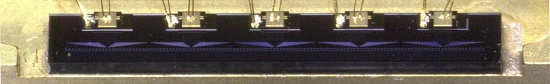
We fabricated a light source with 1000 output ports [
8] in which the silicon optical waveguides were split into eight waveguides by using cascaded 1 × 4 and 1 × 2 multimode interferometer (MMI) splitters and in which five LD array chips with 25 channels were mounted on a silicon waveguide platform by multichip bonding [
4] (
Figure 1). The size of the light source was 9700 μm × 1250 μm. The pitch of the output ports was set to 9 μm in order to include 1000 ports in 1 cm, corresponding to the stepper shot size.
Figure 1.
Microscope image of 1000-channel hybrid integrated light source with waveguide splitters and multiple laser diode (LD) array chips. (a) Overview; (b) Enlargement around mounted LD array.
Figure 1.
Microscope image of 1000-channel hybrid integrated light source with waveguide splitters and multiple laser diode (LD) array chips. (a) Overview; (b) Enlargement around mounted LD array.
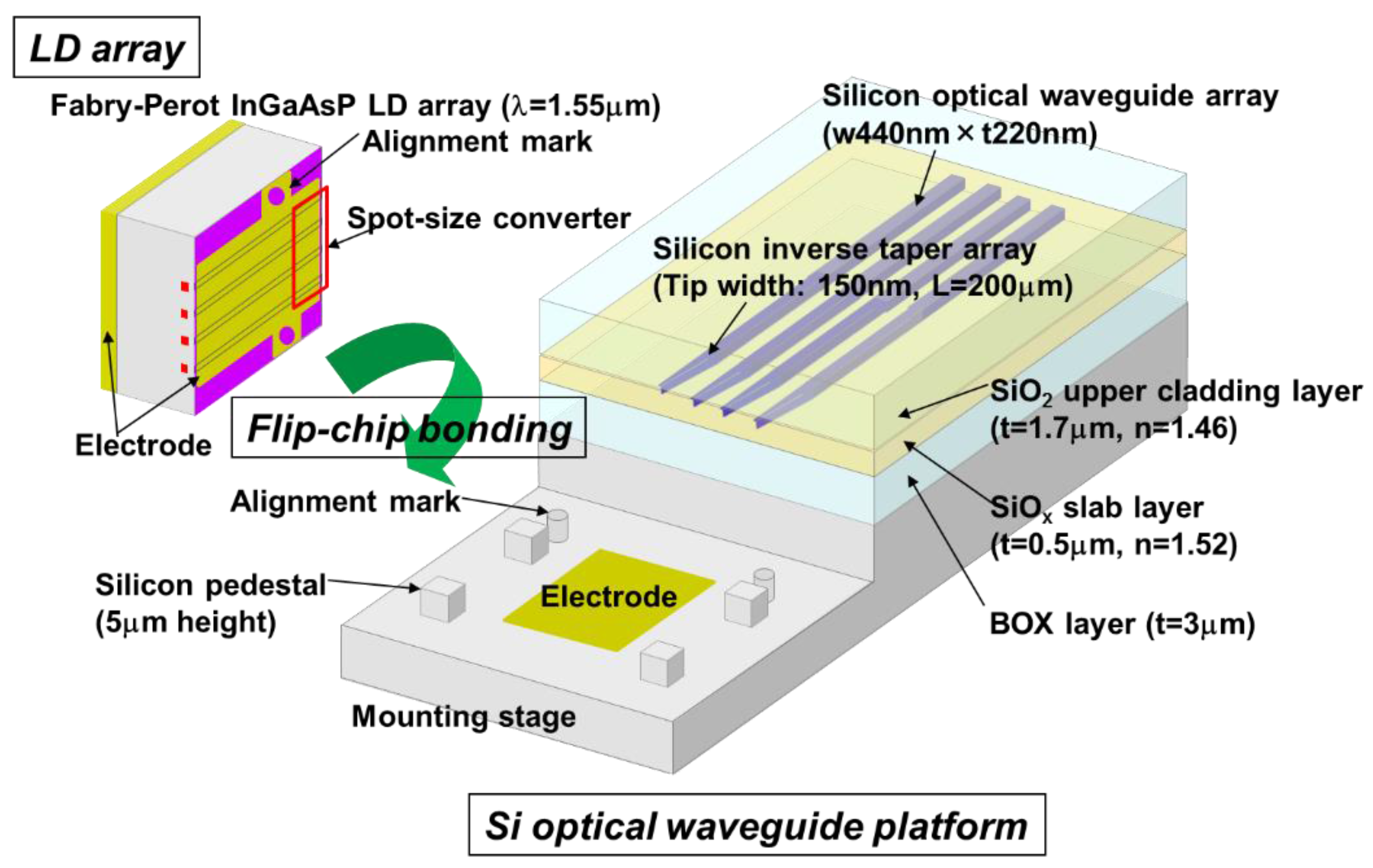
The main structure of the light source is shown in
Figure 2 [
8]. Each LD in the array is a Fabry-Perot (FP) LD with a spot-size converter (SSC) including an inverse taper at the waveguide facet side and has a structure consisting of an InGaAsP base strained multiple-quantum-well buried heterostructure at a lasing wavelength of about 1.55 μm. The LD array chip is 600 μm wide and 400 μm long. The LD array has 25-channel stripes with 15-μm pitches and has alignment marks. The platform consists of silicon optical waveguides with SSCs and an LD mounting stage. The core section of the silicon waveguide is 440 nm wide and 220 nm high using a silicon on insulator (SOI) layer. The tip width and length of the tapered waveguide are 150 nm and 200 μm, respectively. The waveguides include a 0.5-μm-thick SiO
x slab layer with a refractive index of 1.52, a 1.7-μm-thick upper cladding layer with a refractive index of 1.46, and a 3-μm-thick buried oxide (BOX) lower cladding layer. After fabricating the waveguide facet and removing the BOX layer from the mounting area by dry etching, the LD mounting stage has silicon alignment marks and silicon pedestals. An electrode was then formed on the silicon substrate.
Figure 2.
Schematic of hybrid integrated light source with LD array on silicon platform made using SSC with SiOx slab layer.
Figure 2.
Schematic of hybrid integrated light source with LD array on silicon platform made using SSC with SiOx slab layer.
3. Optical Characteristics of the Light Source
We describe the optical characteristics of the light source with 1000 output ports. We obtained the optical power of the 200 outputs at an operation current of ~1 A at each LD array, corresponding to ~40 mA per channel. The relative intensity was normalized by the average power of 200 output ports at each LD array.
On the basis of the relative intensity, we estimated the histograms and standard deviations at each LD array.
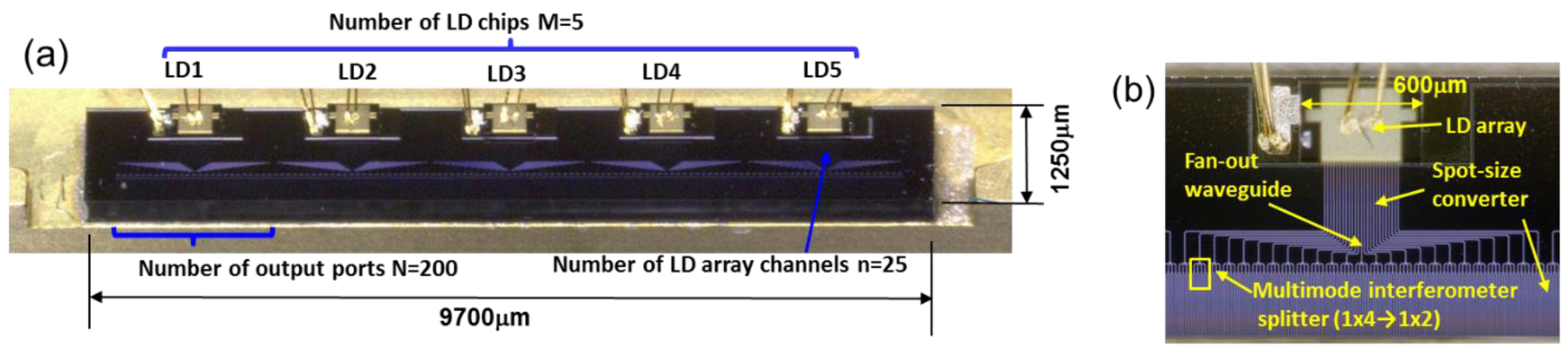
3.1. Power Uniformity by Heat Dissipation through Silicon Substrate
Figure 3a,b show a relative intensity of the 200 waveguide output ports at the first 25-channel LD array without and with a thermal control at a silicon substrate backside temperature of 20 °C. The power uniformity of the relative intensity is improved by thermal control. Since the LD mounting area on the platform was formed by removal of the BOX layer, the thermal impedance is relatively low, and the heat dissipation through the silicon substrate is effectively performed [
8,
9].
Figure 3.
Relative intensity of 200 output ports at a 25-channel LD array (a) without; (b) with a thermal control at a temperature of 20 °C.
Figure 3.
Relative intensity of 200 output ports at a 25-channel LD array (a) without; (b) with a thermal control at a temperature of 20 °C.
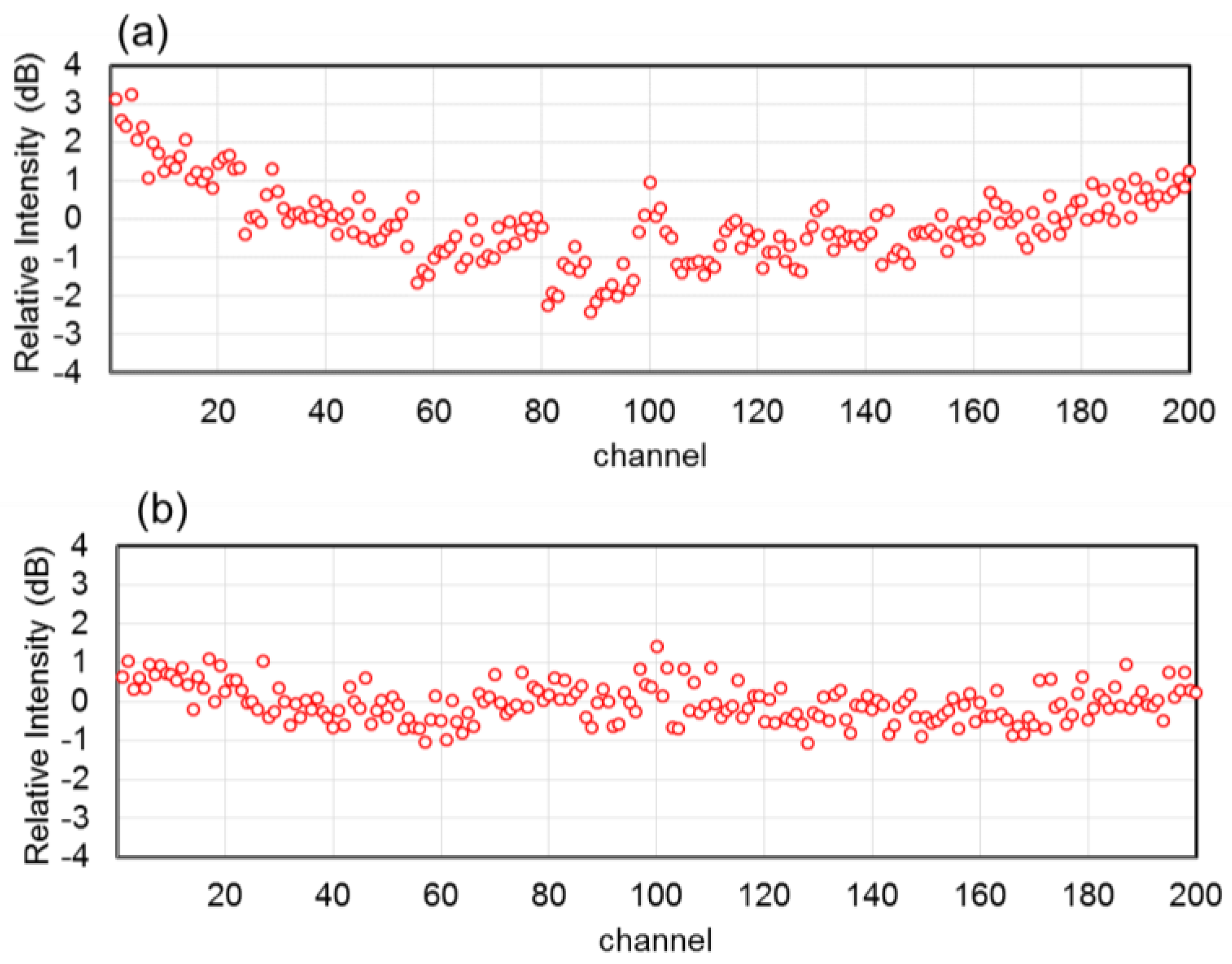
3.2. Power Uniformity of the 1000 Output Ports of the Light Source
Figure 4 shows a relative intensity of the 1000 waveguide output ports in the light source at the silicon substrate backside temperature of 20 °C. Optical outputs of the 1st–200th, 201th–400th, 401th–600th, 601th–800th, and 801th–1000th port at the first, second, third, forth, and fifth LD chip are shown in
Figure 4a–e, respectively.
Figure 4.
Relative intensity of 200 output ports at (a) first LD array; (b) second LD array; (c) third LD array; (d) fourth LD array; (e) fifth LD array.
Figure 4.
Relative intensity of 200 output ports at (a) first LD array; (b) second LD array; (c) third LD array; (d) fourth LD array; (e) fifth LD array.
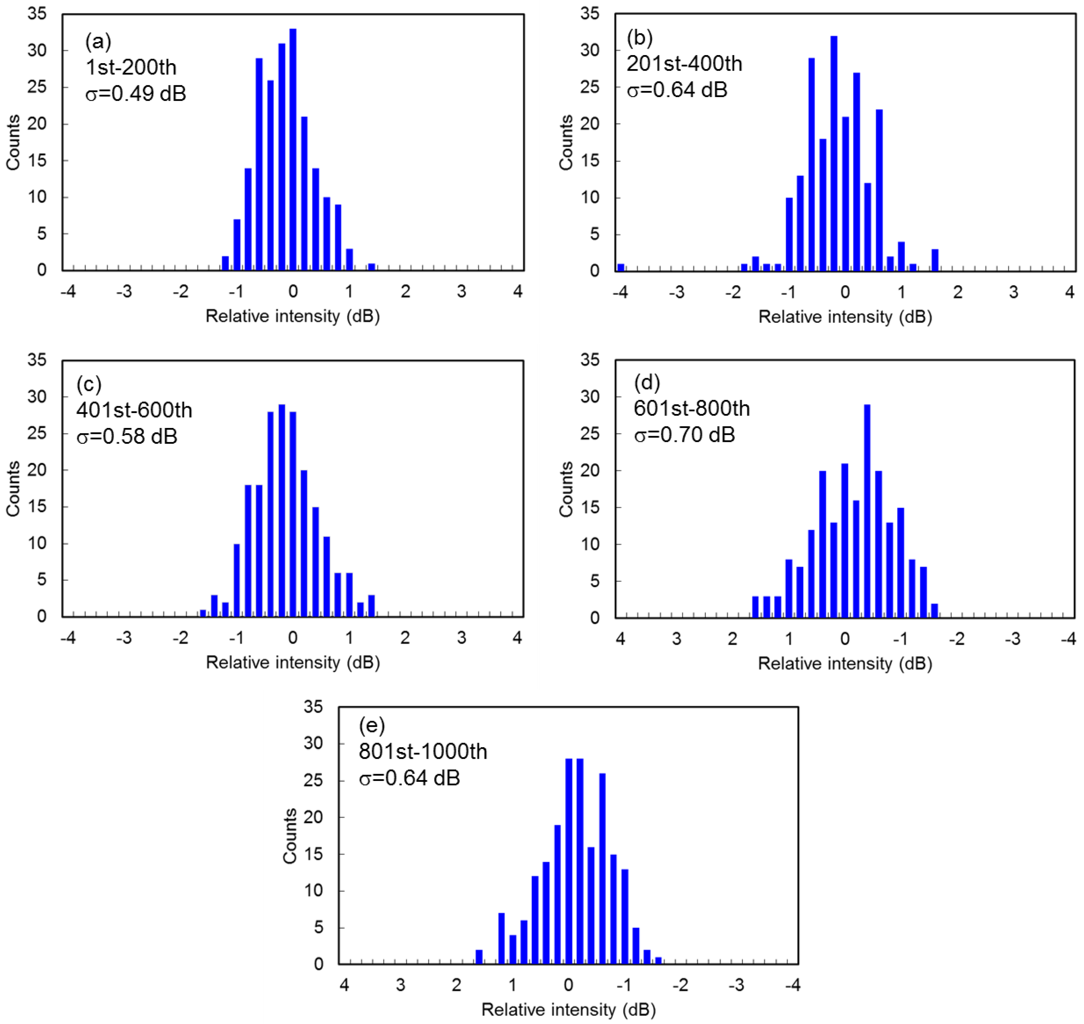
3.3. Histograms of the Output Ports
Figure 5 shows a histogram of the relative intensity of the 1000 output ports, which is based on the results of the relative intensity as shown in
Figure 4. The standard deviations of 200 output ports at the first, second, third, fourth, and fifth LD array are 0.49, 0.64, 0.58, 0.70, and 0.64 dB, respectively. The standard deviation of the histogram is the same as the integrated light source with 104 output ports [
4].
Figure 5.
Histograms of relative intensity of 200 output ports at (a) first LD array; (b) second LD array; (c) third LD array, (d) fourth LD array; (e) fifth LD array.
Figure 5.
Histograms of relative intensity of 200 output ports at (a) first LD array; (b) second LD array; (c) third LD array, (d) fourth LD array; (e) fifth LD array.
4. Discussion of the Power Uniformity of the Light Source
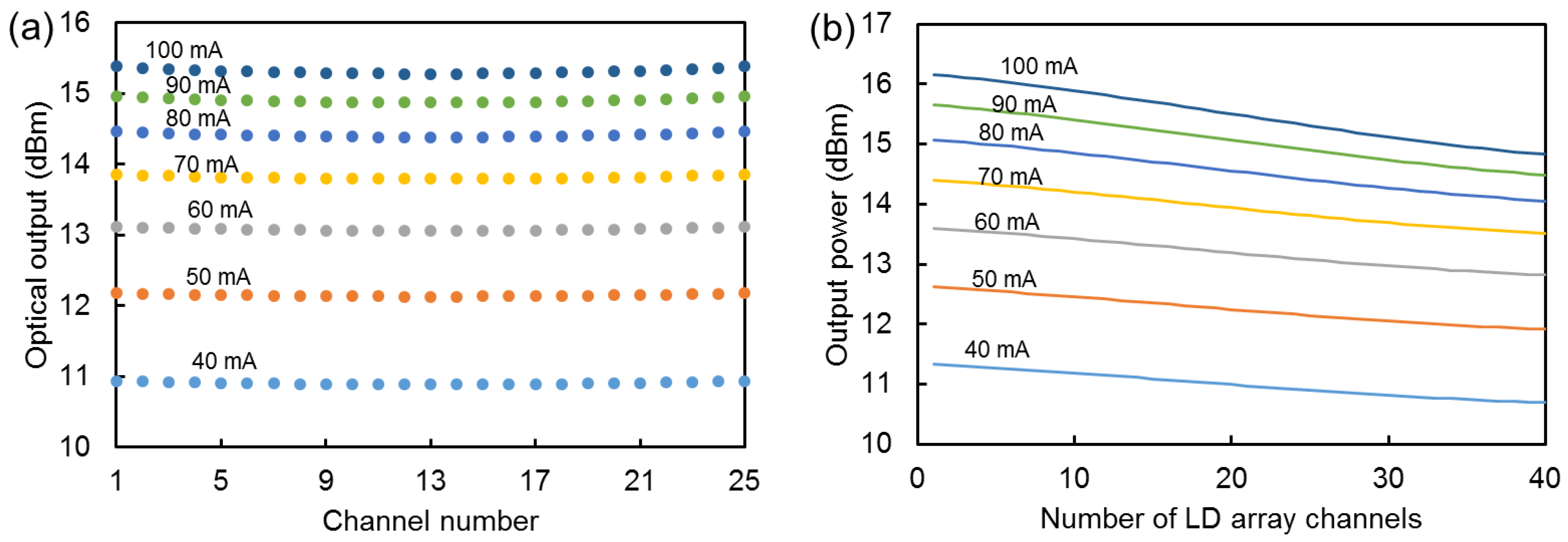
We estimated the power uniformity of the light source. The power and loss budget of the output port consists of the power of the LD array, the coupling loss between the LD array and the waveguide facet, and the waveguide loss including fan-out waveguide and two cascaded MMI couplers.
Figure 6 shows the simulation results of the LD array mounted on a silicon substrate at various injection currents from 40 mA to 100 mA at the silicon substrate backside temperature of 20 °C. The optical output for each channel in the 25-channel LD array considering the thermal interference between channels in the LD array chip is shown in
Figure 6a. The optical power for the central channel against the number of LD array channels is shown in
Figure 6b. While the temperature increase for the central channel (channel 13) was slightly higher than that of the outer channels because of the heat generated from both sides [
8], the optical output of the central channel is slightly lower than that of the outer channel. While the temperature for the central channel was increased with the number of LD array channels, the optical power was decreased with the number of LD array channels.
Figure 6.
Simulation results of LD array at various injection currents. (a) Optical output for each channel in 25-channel LD array considering thermal interference between channels in LD array chip; (b) Optical power for central channel against number of LD array channels.
Figure 6.
Simulation results of LD array at various injection currents. (a) Optical output for each channel in 25-channel LD array considering thermal interference between channels in LD array chip; (b) Optical power for central channel against number of LD array channels.
The coupling loss between the mounted LD array and the waveguide facet formed by dry etching was 2.7 dB, which was almost the same as that of coupling tolerance measurement [
8]. The uniformity of coupling loss was estimated from the output uniformity of the 13-channel LD array and the waveguide output in the integrated light source having the same length of waveguide array which was previously reported such as that the output power uniformity across the output ports was better than 1.3 dB while the output power uniformity across the LD array was better than 0.7 dB [
3,
4]. This uniformity was a result of the simultaneous alignment at the flip-chip bonding.
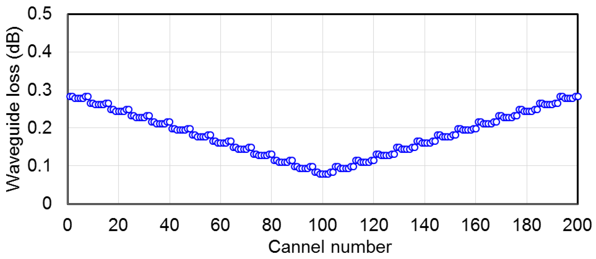
Figure 7.
Waveguide loss of light source including fan-out waveguide for each port in 200 output ports at each LD array.
Figure 7.
Waveguide loss of light source including fan-out waveguide for each port in 200 output ports at each LD array.
Figure 7 shows the waveguide loss of the light source including the fan-out waveguide for each port in 200 output ports at each LD array, corresponding to
Figure 1, while a transmission loss of the waveguide was 2.9 dB/cm. Since the length of the central port waveguide (100th or 101th port) is shorter than that of the outer ports, the waveguide loss is lower than that of the outer ports. The cascaded 1 × 2 and 1 × 4 MMI couplers had a splitting loss of 9 dB and an excess loss of ~1 dB.
Therefore, the power uniformity of the output ports, in particular at the first LD array and the fifth LD array as shown in
Figure 4a,e, can be estimated so that the power of the central channel and the outer channel is slightly higher than that of the other channels. There are several power variation components, but the power uniformity of the light source can be improved by a combination of the layout design and consideration of the thermal interference between the LD array channels. This estimation is also available for various types of hybrid integrated light sources with a LD array on a silicon optical waveguide platform such as the hybrid integrated silicon-photonics-base optical I/O cores [
10].
5. Conclusion
We described the optical characteristics of a multi-channel hybrid integrated light source for an optical interconnection with a bandwidth of over 10 Tbit/s. The power uniformity of the relative intensity of a 1000-channel light source was shown, and it was estimated that the minimum standard deviation σ of the optical power of the 200 output ports at each 25-channel LD array was 0.49 dB. The power uniformity of the light source can be improved by a combination of the layout design and consideration of the thermal interference between the LD array channels. This hybrid integrated light source is expected to be easily adaptable to a photonics-electronics convergence system for ultra-high-bandwidth interchip interconnections.
Acknowledgments
The authors thank Masashige Ishizaka, Makoto Okano, Hiroyuki Takahashi, Tsuyoshi Horikawa, and Masahiko Mori for their fruitful discussions. They also thank Atsuya Kurita, Masataka Noguchi, and Akio Kamei for preparing samples. This research is supported by the Japan Society for the Promotion of Science (JSPS) through its “Funding Program for World-Leading Innovative R&D on Science and Technology (FIRST Program)” initiated by the Council for Science and Technology Policy (CSTP). This research is also supported by the New Energy and Industrial Technology Development Organization (NEDO). Part of this work was conducted at the Tsukuba Innovation Arena Super Clean Room (TIA-SCR) by the National Institute of Advanced Industrial Science and Technology (AIST).
Author Contributions
T.S., N.H., and M.K. performed the device design, device fabrication, and experiments. T.S., N.H., Y.U., T.Y., T.N., and Y.A. discussed the results and co-wrote the manuscript. Y.A. supervised the research.
Conflicts of Interest
The authors declare no conflict of interest.
References
- Arakawa, Y.; Nakamura, T.; Urino, Y.; Fujita, T. Silicon Photonics for Next Generation System Integration Platform. IEEE Commun. Mag. 2013, 51, 72–77. [Google Scholar] [CrossRef]
- Urino, Y.; Usuki, T.; Fujikata, J.; Ishizaka, M.; Yamada, K.; Horikawa, T.; Nakamura, T.; Arakawa, Y. High-Density and Wide-Bandwidth Optical Interconnects with Silicon Optical Interposers. Photon. Res. 2014, 2, A1–A7. [Google Scholar] [CrossRef]
- Shimizu, T.; Hatori, N.; Okano, M.; Ishizaka, M.; Urino, Y.; Yamamoto, T.; Mori, M.; Nakamura, T.; Arakawa, Y. High Density Hybrid Integrated Light Source with a Laser Diode Array on a Silicon Waveguide Platform for Inter-Chip Optical Interconnection. In Proceedings of the IEEE International Conference on Group IV Photonics, London, UK, 14–16 September 2011.
- Shimizu, T.; Hatori, N.; Okano, M.; Ishizaka, M.; Urino, Y.; Yamamoto, T.; Mori, M.; Nakamura, T.; Arakawa, Y. Multichannel and High-Density Hybrid Integrated Light Source with a Laser Diode Array on a Silicon Optical Waveguide Platform for Inter-chip Optical Interconnection. Photon. Res. 2014, 2, A19–A24. [Google Scholar] [CrossRef]
- Hatori, N.; Shimizu, T.; Okano, M.; Ishizaka, M.; Yamamoto, T.; Urino, Y.; Mori, M.; Nakamura, T.; Arakawa, Y. Hybrid Integrated Light Source on a Silicon Platform Using a Trident Spot-Size Converter. J. Lightwave Technol. 2014, 32, 1329–1336. [Google Scholar] [CrossRef]
- Shimizu, T.; Okano, M.; Takahashi, H.; Hatori, N.; Ishizaka, M.; Yamamoto, T.; Mori, M.; Nakamura, T.; Arakawa, Y. Demonstration of over 1000-Channel Hybrid Integrated Light Source for Ultra-High Bandwidth Inter-Chip Optical Interconnection. In Proceedings of the Optical Fiber Communication Conference and Exposition, San Francisco, CA, USA, 9–14 March 2014.
- Shimizu, T.; Okano, M.; Takahashi, H.; Hatori, N.; Ishizaka, M.; Yamamoto, T.; Mori, M.; Horikawa, T.; Urino, Y.; Nakamura, T.; et al. Multi-Channel and High-Density Hybrid Integrated Light Source by Thermal Management to Low Power Consumption for Ultra-high Bandwidth Optical Interconnection. In Proceedings of the International Conference on Electronics Packaging, Toyama, Japan, 23–25 April 2014.
- Shimizu, T.; Ishizaka, M.; Hatori, N.; Okano, M.; Yamamoto, T.; Mori, M.; Urino, Y.; Nakamura, T.; Arakawa, Y. Multi-channel Hybrid Integrated Light Source for Ultra-high-bandwidth Optical Interconnection and Its Structural Optimization for Low Power Consumption by Considering Thermal Interference between LD Arrays. Trans. Jpn. Inst. Electron. Packag. 2014, 7, 94–103. [Google Scholar] [CrossRef]
- Hatori, N.; Shimizu, T.; Okano, M.; Yamamoto, T.; Urino, Y.; Mori, M.; Nakamura, T.; Arakawa, Y. Theoretical and experimental thermal analysis of a hybrid integrated light source. In Proceedings of the 4th International Symposium on Photonics Electronics Convergence, Tokyo, Japan, 17–19 November 2014; p. 35.
- Yashiki, K.; Suzuki, Y.; Hagihara, Y.; Kurihara, M.; Tokushima, M.; Fujikata, J.; Ukita, A.; Takemura, K.; Shimizu, T.; Okamoto, D.; et al. 5 mW/Gbps hybrid-integrated Si-photonics-based optical I/O cores and their 25-Gbps/ch error-free operation with over 300-m MMF. In Proceedings of the Optical Fiber Communication Conference and Exposition, Los Angeles, CA, USA, 22–26 March 2015.
© 2015 by the authors; licensee MDPI, Basel, Switzerland. This article is an open access article distributed under the terms and conditions of the Creative Commons Attribution license (http://creativecommons.org/licenses/by/4.0/).
