Article

Transient Response of Organo-Metal-Halide Solar Cells Analyzed by Time-Resolved Current-Voltage Measurements

by
M. Greyson Christoforo
1,†,
Eric T. Hoke
2,
Michael D. McGehee
2 and
Eva L. Unger
3,*
1
Department of Electrical Engineering, Stanford University, Stanford, CA 94305, USA
2
Department of Materials Science an Engineering, Stanford University, Stanford, CA 94305, USA
3
Department of Chemistry, Lund University, 22241 Lund, Sweden
*
Author to whom correspondence should be addressed.
Present address: University of Oxford, Physics Department, Clarendon Laboratory, Parks Road, OX1 3PU, Oxford, UK.
Photonics 2015, 2(4), 1101-1115; https://doi.org/10.3390/photonics2041101
Submission received: 3 November 2015 / Revised: 18 November 2015 / Accepted: 19 November 2015 / Published: 24 November 2015
(This article belongs to the Special Issue Perovskite Photovoltaic and Optoelectronics)

Abstract

:
The determination of the power conversion efficiency of solar cells based on organo-metal-halides is subject to an ongoing debate. As solar cell devices may exhibit very slow transient response, current-voltage scans in different directions may not be congruent, which is an effect often referred to as hysteresis. We here discuss time-resolved current-voltage measurements as a means to evaluate appropriate delay times (voltage settling times) to be used in current-voltage measurements of solar cells. Furthermore, this method allows the analysis of transient current response to extract time constants that can be used to compare characteristic differences between devices of varying architecture types, selective contacts and changes in devices due to storage or degradation conditions.

Graphical Abstract

1. Introduction

The reported device efficiencies of solar cells based on the organo-metal-halide methylammonium lead iodide have increased at an unprecedented pace during the past three years. Impressive performance improvements have been achieved in different device architectures [1,2,3,4] by refinement of the deposition methods of the organo-metal-halide perovskite (OMHP) absorber [4,5,6,7,8] and optimization of selective contact layers [9,10,11]. Determining the steady state power conversion efficiency of solar cell devices based on these novel absorber materials reliably has been to be non-trivial [12,13,14,15].
When the voltage applied across these devices is abruptly changed, the current through the device is often slow to respond, i.e., the corresponding change in current lags behind the change in voltage. These transients in the response can occur on different time scales and often manifest themselves as discrepancies between the forward and reverse current-voltage scans of solar cells, an embodiment which the community commonly refers to as “hysteresis” [12,13,16,17,18,19]. If not taken into account, this “hysteretic” behavior can result in significant over- or underestimation of the solar cell’s power conversion efficiency. The absence of hysteresis, i.e., a negligible discrepancy between current-voltage curves when the devices are scanned in the forward and reverse directions, does not guarantee that measurements have been performed correctly. Congruency between forward and reverse scans has been shown both for very short delay times and very long delay times during the current-voltage scan. The delay time or voltage settling time refers to the time delay after a voltage step before the current is sampled [12]. This has caused debate about how to determine the power conversion efficiencies of solar cell device based on organo-metal-halide materials reliably. Slow transient effects in the current-voltage response of solar cell devices are not unique to OMHP-based devices and have also been observed for dye-sensitized solar cells [20]. Recommended measuring protocols have been outlined elsewhere [12,13,21].
Meanwhile, several phenomenological observations on the occurrence or absence of “hysteresis” are important indications of underlying physical phenomena that cause these transient effects. Planar hetero-junction thin film devices are often found to exhibit a more severe hysteresis compared to devices based on meso-porous titanium dioxide [12]. In the latter, thicker meso-porous TiO2 layers were shown to further reduce hysteresis [19]. In samples with an insulating Al2O3 network, on the other hand, severe hysteresis is observed [16,22]. In planar hetero-junction devices, a larger average crystallite size of the organo-metal-halide domains [19], as well as the choice of selective contacts [23,24,25,26,27,28,29] were found to reduce or eliminate hysteresis all together and yield a stable high power conversion efficiency. Often, the only criteria that is analyzed is the presence or absence of “hysteresis”, i.e., the congruency between IV-scans in different scan directions, at one single delay time. This is however not sufficient, as OMHP based devices can sometimes be measured “hysteresis-free” or “hysteresis-less” in different time domains, i.e., at different delay times [12]. Devices exhibiting no hysteresis at room temperature conditions may exhibit hysteresis at lower temperature, when processes causing transients slow down [14]. This illustrates, that transient phenomena need to be thoroughly investigated and commented on when stating device performance metrics derived from current-voltage measurements.
The physical origin of the hysteresis in perovskite solar cells is currently under investigation. Research is ongoing to understand the role of charge carrier accumulation in trap states causing chemical capacitive effects [16,30,31,32], the possibility of a ferroelectric polarizability due to re-orientation of methylammonia cations within the crystal cage [32,33,34,35,36,37,38,39,40], and ion migration causing a change in electric field distribution within the active layer and self-doping effects [22,41,42,43]. While capacitive effects due to the trapping and de-trapping of charge carriers are found to occur [30,44], the magnitude of the transient current and voltage response is too large to be caused by chemical capacitive effects alone [12,30]. Various recent contributions have illuminated, that the extraction of photogenerated charge carriers seems indeed more efficient after devices are poled/polarized [13,22,30] at forward bias, for which the more generic term: temporary enhanced by bias (TEBBed) has been suggested [30]. Migration of ionic species has been proven to occur in methylammonium-lead-iodide (MAPI) and related materials, whereof halide vacancies are the most likely to form and migrate [22,43,45,46,47,48]. The intrinsic defect density and chemistry is critically influenced by the materials deposition and processing conditions [49,50,51,52,53]. Experimental evidence corroborates that the re-distribution of charged defects under an applied electric field causes a change in the internal potential gradient, resulting in a temporary p-i-n or p-n homo-junction in the MAPI layer that explains the temporarily enhanced charge carrier extraction efficiency [22,30,42,52].
The observed transients in the current-voltage response are very likely related to temporal and bias-dependent changes in the distribution of charged defects in the absorber layer. Systematic methods to quantify and distinguish between transient effects are needed to further our understanding of the electronic and chemical processes in solar cell devices based on OMHPs. One metric used to quantify the difference between the forward and reverse IV-scan is the hysteresis index, i.e., the difference in the current generated at 80% of the VOC between the reverse and forward scan direction divided by the current measured at this voltage in the reverse scan direction [19]. However, this metric is not well-defined since the “hysteresis index” is typically highly dependent on the voltage scan rate: for example negligible discrepancy between the forward and reverse scan direction can often be obtained at both extremely short (ms) and very long (>1 s) delay times while pronounced “hysteresis” is observed at intermediate times [12]. One of the most reliable ways to compare device performance is tracking their steady-state power conversion efficiency over time [12,16].
Time-resolved staircase voltammetry measurements are a valuable mean to monitor the current response during a voltage step (Figure 1) and from this evaluate appropriate delay times for current-voltage measurements to ensure that measurements are carried out under steady-state conditions [12]. This profile of consecutive applied potentials can also be referred to as a (linear) staircase sweep [53] and is commonly employed to evade the contribution of capacitive charging events when analyzing electrochemical systems. We, herein, highlight the unique picture and insight into a solar cell’s dynamic response that can be gained by continuously recording the current through the cell during a voltage staircase sweep, that we will be referring to as I,V(t)-measurements. This method is in contrast to the typical I(V)-measurement that only records one value of current for each step in voltage. I,V(t) measurements are particularly useful to quantify “memory” or “hysteresis” effects in solar cells based on OMHPs and allow the determination of the minimum delay time to reach steady-state during a regular I(V)-measurements as visualized in Figure 1. Since the current is being continuously recorded, we can in principle derive the resulting I(V)-curve for any delay time through data processing. Furthermore, the time constants of the current transients in each segment can be extracted and compared as a function of voltage. Additionally, integrated currents in each voltage segment can be compared to evaluate changes in the internal electric field of the devices caused by light-soaking and/or applied potentials (TEBBing [31]).
To perform the measurements described herein, we wrote a measurement routine to control a Keithley 2400 sourcemeter in the Python programming language [54]. A MATLAB script was used to extract and analyze the I,V(t)-data generated [55]. Both scripts are freely available on the web. We hope this code will be useful to other researchers in the community and we welcome additions and improvements to it.

2. Experimental Section

The device data shown herein was acquired on solution-processed thin film solar cell devices prepared and tested within the scope of our previous report and devices were fabricated as described therein [12] In short, the n-type selective contact was a titanium dioxide layer, prepared by spray-pyrolysis deposition of a diluted solution of Titanium-di(isopropoxid)-bis(acetylacetonate) (Aldrich) onto a fluorine-doped tin oxide glass substrate (Pilkington, TEC15). Methylammonium-lead-iodide (MAPbI3) was deposited from a solution containing three equivalents of the methylammonium iodide (MAI) and lead chloride (PbCl2) precursors, with MAPbI3 being formed upon sublimation of methylammonium chloride (MACl) during annealing at 100 °C for 45 min [56]. The p-type contact was established by spin-coating a solution of spiro-OMeTAD, the oxidized analogue spiro(TFSI)2 and the additives lithium-trifluoro and tBP [57]. A gold back contact of 0.2 cm−2 was deposited by thermal evaporation. For measurements, solar cells were masked with an aperture of 0.12 cm−2 defining the active area. Prior and between measurements, samples were stored in a dry, dark environment. The effect of conditions prior to the measurements will be discussed in the Results and Discussion section.
Current response during staircase voltage sweeps, I,V(t) measurements, were measured under simulated AM1.5 solar irradiation from a solar simulator (Newport). The device area was defined by using a shadow mask with an area similar in size to the active area of the evaporated metal contact. In a typical measurement, the voltage across the cell was stepped from short-circuit to a forward bias of at least 1.1 V (forward scan), or from forward bias to 0 V (reverse scan) in 50 mV increments with a 15 s dwell time during each step and a current and voltage measurement sampling rate of about 140 Hz. In each voltage segment, both for current and voltage, roughly 2100 values are hence recorded. The ultimate output of this measurement contains three data columns: time, voltage and current. Figure 1 shows the I(t) and V(t) (staircase profile) on a shared time axis. Data analysis was carried out with a MATLAB script that allowed us to plot the resulting I(V) curve as a function of delay time (Figure 2d). Furthermore, the current response in each constant voltage segment can be analyzed by fitting to a characteristic equation (using a Non-linear Least Squares method). For the data analysis performed herein, a bi-exponential was found to fit the transient current data reasonably well, although some other equation may well be more appropriate to describe the underlying physical processes causing the transients. Integration of the transient current response allowed us to visualize at which applied potentials the transient response causes the largest discrepancy with respect to the steady state response of the solar cell device.

3. Results and Discussion

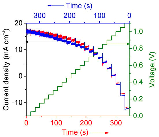
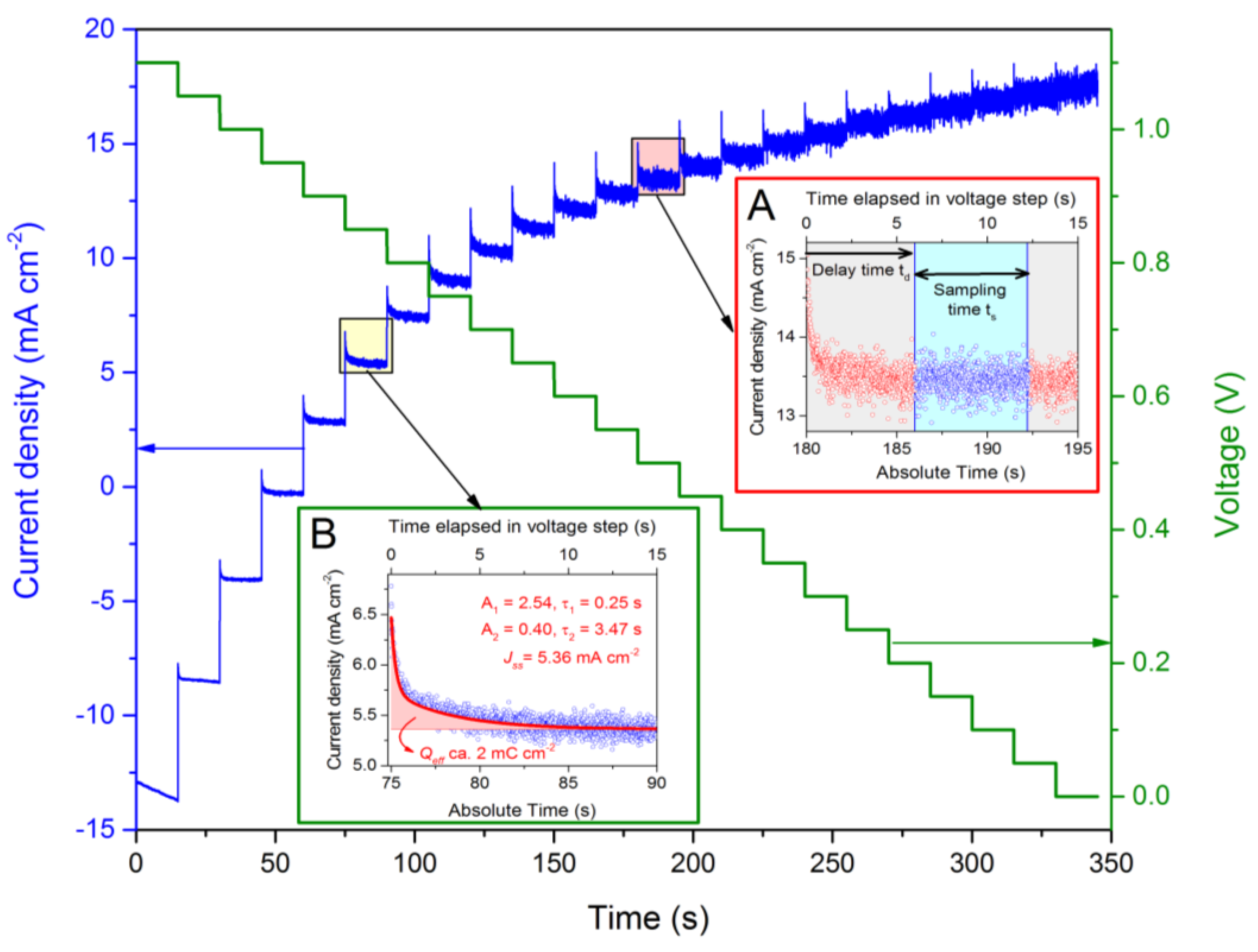
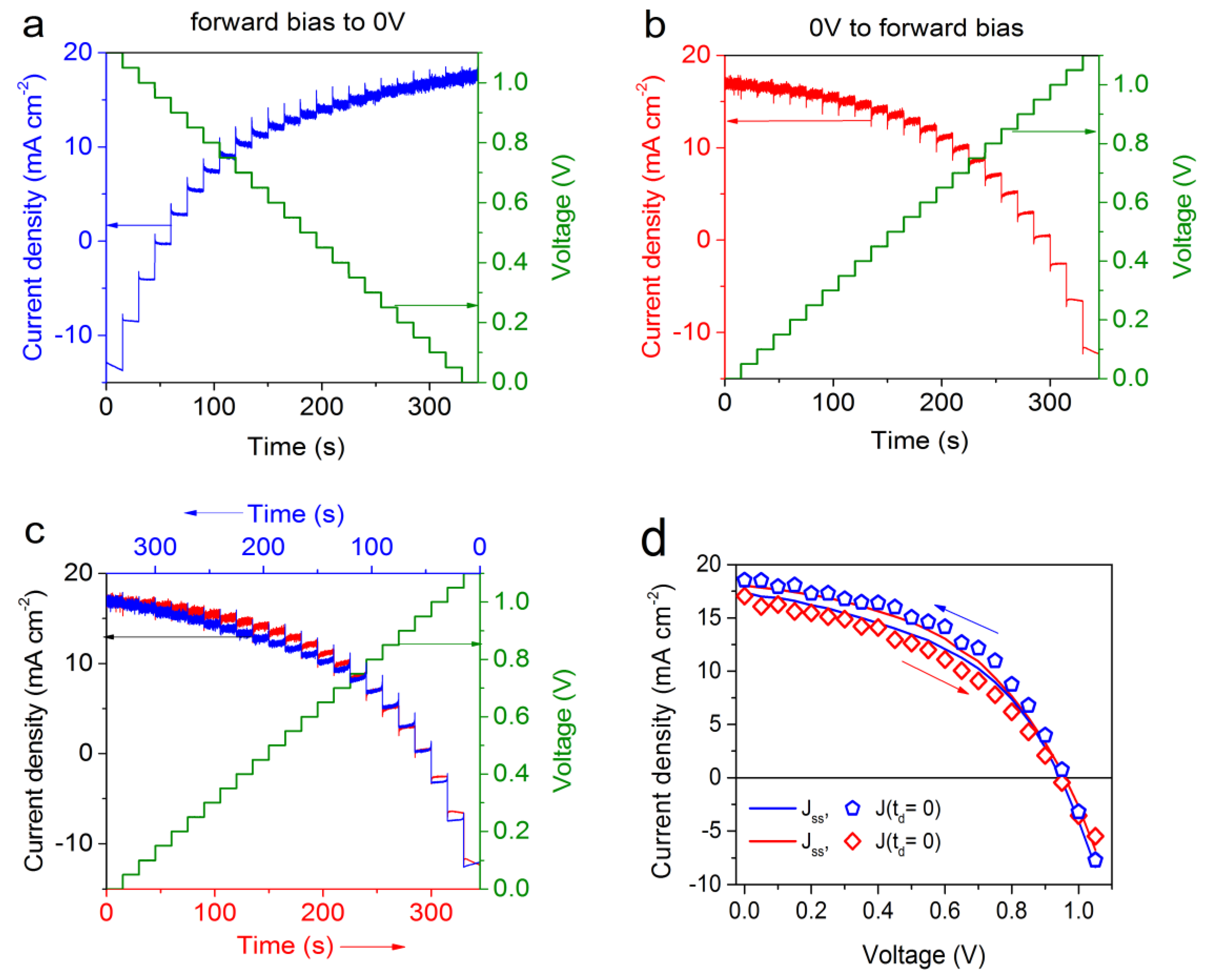
3.1. Time-Resolved Current-Voltage-Measurements

Figure 1 shows typical output data from the I,V(t) measurement. This particular scan was a reverse scan (from forward bias to 0 V) performed in voltage steps of 50 mV and with a dwell time of 15 s after each step. The I,V(t) measurement provides a unique picture of the solar cell’s dynamic operating characteristics since it captures the transient decays or rises in current in response to the step changes in voltage. These dynamics are not captured by conventional I(V) measurements. The I(V) plot can be derived by averaging the current over a defined sampling time ts after waiting a defined delay time td (Figure 1, inset A) after each voltage step. The delay gives the current time to settle to a constant value, which avoids distortion of the resulting I(V) data due to capacitive charging or discharging currents. Delay times td typically on the order of 10 seconds are required to avoid distortions of the IV-curve due to transient effects commonly observed in perovskite devices.
Figure 1. Transient current-density (left axis) response as a function of time (x-axis) in response to a staircase voltage sweep (right axis) from 1.1 V to 0 V (reverse scan direction). The current density exhibits visible overshoots followed by a slow decay in each voltage segment. Inset (A) highlights that both the delay time td and sampling time ts influence the current recorded during a regular I(V) measurement. Inset (B) illustrates the possibility to analyze each individual voltage segment to extract characteristic time constants, (τ1 and τ2), pre-exponential factors (A1 and A2), the steady state current (Jss) and integrated current density yielding the effective displacement charge density (Qeff).
Photonics 02 01101 g001
Familiar I(V) characterization curves can be recreated from the I(V,t) dataset analytically by choosing td, and ts, as illustrated in Figure 1, inset (A). The impact of both td and ts on the resulting I(V) curve can then be evaluated. While seemingly more time consuming and complicated than a simple I(V) sweep, one should consider the wealth of information collected in a single I,V(t) measurement. We found this procedure indeed to be less time consuming than trying to find an optimal scan rate by iteratively increasing the delay time in a regular I(V) measurements until negligible discrepancy between forward and reverse scan direction was reached. Importantly, the I,V(t) measurement gives a clear indication of the time scale and magnitude of transient effects in the solar cell devices.
The data shown here illustrates that for this particular thin film solar cell device based on methylammonium-lead-iodide with an n-selective titania and a p-selective spiro-MeOTAD contact, the response of the photocurrent to a change in applied potential is very slow and a td > 5 s should be employed. A shorter td would have resulted in a substantially higher photocurrent, especially around the maximum power point, for the device scanned in the reverse scan direction.
In Figure 2, we compare the I,V(t) measurements of the same devices in the reverse (a, equal to Figure 1) and forward (b) scan direction. The forward scan exhibits the opposite transient response compared to the reverse scan exhibiting an immediate drop and subsequent exponential rise in the photocurrent in each voltage segment. In Figure 2c, the two measurements were combined into one graph by reversing the time-axis for the reverse scan. We chose to discuss this example as it illustrates, that the steady state current densities, Jss, are not superimposed between 0.4 V and 0.8 V for the reverse and forward scan with the forward scan exhibiting slightly higher values for Jss. While this may be considered a negative example it highlights an important phenomena: The I(V)-characteristics of OMHP based solar cells depend on their measurement history and may change during the measurement.
Figure 2. I,V(t) scan in the reverse scan direction (a) exhibits an over-shoot followed by a transient decay while in the forward scan direction (b) the photocurrent drops followed by an exponential increase during each potential step. The overlay of both data set in (c) was created by reversing the time axis for the forward scan. Plot (d) shows the resulting I(V) curves derived from the I,V(t) plots (a–c) using either the steady-state current density, Jss, or the current density at negligible delay time J(td = 0) for the current density.
Photonics 02 01101 g002
Figure 2d shows I(V) curves generated from the the I,V(t) data both for the the forward and reverse scans shown in plots a and b. The circles correspond to the first measurement point at td = 0 and ts = 0 while the lines represent the resulting steady-state current density Jss by fitting the current transients to Equation (1). Apparently, the steady state current density Jss does not converge for the forward and reverse scan with the forward scan leading to larger values of Jss compared to the reverse scan. Metrics for the power conversion efficiency may hence vary greatly depending on the measurement conditions, in this case from 6.7% to 8.5%.
To rationalize the higher steady state current density measured in the forward scan we would like to note that the forward scan was in this case performed immediately after the reverse scan. The results are evidently influenced by the measurement history of the device, which may be the result of ion redistribution or other effects leading to changes in the internal field distribution [22,30,42,52] causing differences in the charge carrier extraction efficiency. Additionally, the temperature of the device may have increased during the prolonged measurements under illumination, leading to a higher current density. This example demonstrates that true steady-state conditions are indeed very difficult to achieve and maintain in methylammonium-lead-iodide based solar cells. We found the staircase voltammetry measurements shown here to be instrumental in identifying both the fast, multi-time scale transient dynamics following each voltage segment as well as the slower, transients taking place over the course of minutes that are apparent in discrepancies between consecutive staircase sequence measurements. These results emphasize the importance of performing measurements rigorously, providing detailed information on the measurement routines employed, commenting on the measurement history of a device and, very importantly, also commenting on possible deviations from an ideal or consistent behavior as this may offer important indications on the long term stability of the devices.
In this context, we would also like to re-iterate the often ignored difference between the scan rate and the delay time when specifying the experimental conditions used for I(V) measurements. The scan rate of any I(V) measurement is defined by the voltage step size and dwell time in each voltage step. For the measurement shown in Figure 1 the scan rate is hence 3.33 mV/s (50 mV/15 s), independently of which td is used. We therefore recommend stating the delay time and step size rather than scan rate when specifying experimental I(V) measurement conditions. Another remark: there is no optimal or default delay time appropriate for measuring all solar cells. For solar cells based on OMHPs in particular, the minimum td to measure devices under quasi-steady-state conditions is strongly architecture and device dependent and should be re-evaluated every time. In this regard, the I,V(t) measurement is both a means to determine the minimum td and also capture and analyze the devices transient response, which may provide insight into differences between device types, effects of selective contacts, device polarization (TEBBing), light-soaking and degradation effects among other things.

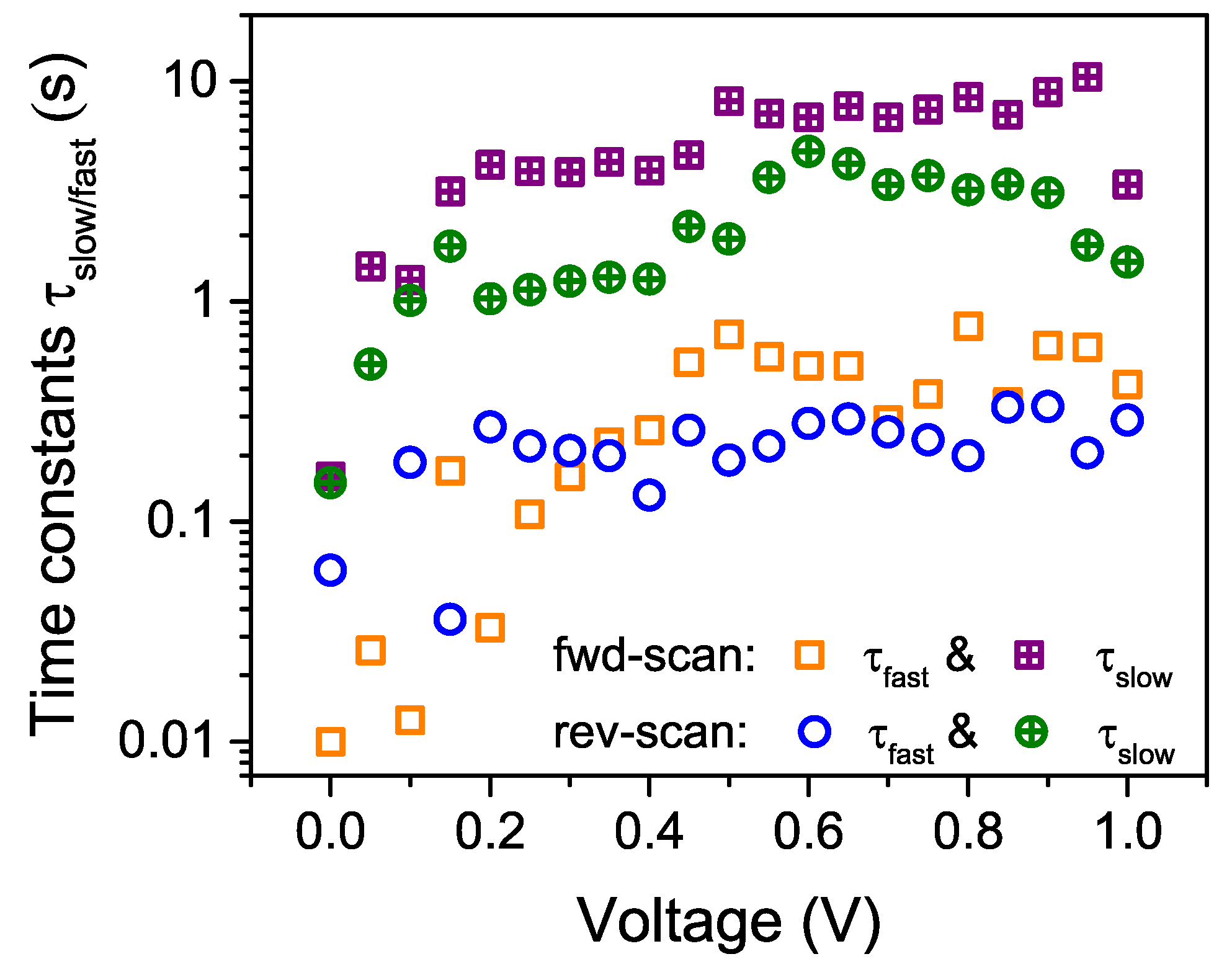
3.2. Analysis of the Transient Response

As indicated in Figure 1, inset (B), the transient current response in each voltage segment can be analyzed further by fitting the experimental data. We found that a bi-exponential fit is fairly adequate to capture the device’s transient current response to a step change in voltage:
J ( t ) = J s s + A 1 exp ( t t 0 τ 1 ) + A 2 exp ( t t 0 τ 2 )
Here t0 is the time at the beginning of each voltage segment, Jss is the aforementioned steady-state current, τ1 and τ2 are the characteristic time constants, and A1 and A2 are exponential scaling factors. For the forward scan, the scaling factors A1 and A2 adopt negative signs as the equation describes an exponential rise rather than decay for the scan in forward direction (see Figure 2b). Note that while we’ve found empirically that a bi-exponential function fits the data quite well, other fit functions or combinations of fit functions may be more suitable to describe the underlying physical phenomena causing the transient current response. As discussed recently in the literature, ion migration is the likely cause for the observed transients as they affect the device polarization [43].
With the bi-exponential fit to fit our experimental data (1), we can extract two time constants that we refer to as τfast and τslow, which we attribute to two distinct physical processes with obvious differences in rate. In Figure 3, we compare the time constant for the forward (fwd) and reverse (rev) scan as a function of the applied voltage. The fast τfast and slow time τslow constants are of a similar order of magnitude for both scan directions with the slow time constants τslow being approximately an order magnitude longer compared to τfast. Both τslow and τfast exhibit a dependency on the applied potentials, becoming shorter towards short circuit. In direct comparison, the τslow here appears to be a factor of 2–4 longer for the forward compared to the reverse scan while τfast appears to depend much less on the scan direction. Note that the forward scan was carried out after the reverse scan.
Figure 3. Fast and slow time constants (τfast and τslow) extracted by fitting the transient current response in each voltage segment to the bi-exponential fit function given in Equation (1) both for the forward (fwd) scan and for the reverse (rev) scan direction.
Photonics 02 01101 g003
The magnitude of τslow is comparable to the characteristic slow time constants extracted by Ono et al. [53], who performed a similar analysis on OMHP solar cells based on meso-porous titanium dioxide electrodes. They attributed the slow time constant to the change in device polarization due to the ferroelectric properties of the OMHP materials. Ferroelectric polarization due to the re-orientation of the methylammonium cation in the inorganic lattice has been discussed as one possible cause for the hysteresis phenomenon [16,17,39]. However, recent publications on this topic have highlighted that the time scale of molecular re-orientation should be on the pico-second time scale [58] and is hence unlikely to be the cause for the transient phenomena occurring on a second time scale. Dipole reorientation may however affect the band structure and possibly charge carrier dynamics in methyl-ammonium-lead-halides [36,37,59].
Our interpretation of the slow transient is more in line with changes in the internal electric field in the OMHP absorber layer due to electrode polarization caused by redistribution of ionic constituents [13,14,38,46,60]. Migrating halide vacancies in the absorber layer under bias can reasonably cause self-doping effects at the selective contacts transiently forming a p-i-n homo-junction that facilitates charge carrier extraction [22,43,46]. Ionic vacancies are both likely to influence the electric field distribution in the absorber and cause self-doping but could simultaneously also act as charge carrier trapping sites.
The transients in the photocurrent cannot hence be attributed to capacitive charging or discharging currents. Integration of the current transient does not give values representative of capacitive charge carrier densities stored in the device. However, integration of the transient portion of the current response can give insight into the voltages at which the device response is most affected by transient phenomena. In Figure 4, we show the integrated current density from each voltage segment for the reverse (squares) as well as the forward scan (circles) distinguishing between the corresponding integrated current for the fast (open symbols) and slow time constants (plus symbols). This plot illustrates that it is predominantly the slow process that causes the discrepancy in the current-voltage response and that the effect is approximately symmetrical, peaking close to 0.7 V, for the reverse and forward scan. The latter exhibits a negative signal as the transient is negative with respect to the steady state current as shown in Figure 2b. Noticeably, the magnitude of the integrated current is almost twice as large for the forward scan compared to the reverse scan. For the data shown here, the forward scan was carried out after the reverse scan. We find that the magnitude of the integrated current density transient depends on the conditions the devices was exposed to for a significant time prior to the start of the measurement. These results highlight, that devices change dynamically in response to bias or light. Storage and conditions prior to the current-voltage measurements can have a dramatic influence on the transient response of the device as the distribution of ionic species may indeed be quite different.
Figure 4. Fast and slow time constants (τfast and τslow) extracted by fitting the transient current response in each voltage segment to the bi-exponential fit function given in Equation (1) both for the forward scan and for the reverse scan direction.
Photonics 02 01101 g004

4. Conclusions

Evidently, it is not trivial to find reliable measurement conditions and protocols to determine the current-voltage response and derive performance metrics for solar cells based on organo-metal-halide semiconductors. We found that the staircase voltammetry measurement routine described herein provides a method for both characterizing and visualizing the transient response of solar cells during I(V) measurements and for determining appropriate measurement delay times that are sufficiently long to produce quasi-steady-state conditions in the device for current-voltage measurements. The data shown here highlights that the time constants of processes causing the slow transient response in solar cells based on MAPbI3 are strongly affected by prior measurements and storage conditions (light, bias, etc.) and that the devices dynamically change during a current-voltage scan. This creates a considerable uncertainty when defining the “stabilized” power conversion efficiency of solar cells based on an I(V) sweep of an OMHP based solar cell. It is important to remember that solar cells are expected to operate at their stated performance specifications for tens of years after installation. Intelligent tracking of the device’s maximum power point performed under continuous full illumination for an extended period of time is most certainly the most honest and accurate way to evaluate the performance and stability of these solar cells. Evaluation of the time constants and the magnitude of transient currents during current-voltage measurements as described herein will prove useful in comparing devices of different architecture types and contact layers and can also give insight into changes in devices during degradation or due to previous exposure conditions.

Acknowledgments

E.L.U. thanks the Marcus and Amalia Wallenberg memorial fund for a postdoctoral research fellowship. Experimental work was funded by the Global Climate and Energy Project (GCEP). M.G.C. has received funding from the European Union’s Horizon 2020 research and innovation programme under the Marie Skłodowska-Curie grant agreement No 659667. This work reflects only the author’s viewand that the EU is not liable for any use that may be made of theinformation contained therein.

Author Contributions

E.L.U. conceived the measurement methodology, performed experiments and data analysis and was the main responsible for writing this manuscript; M.G.C. programmed the python scan routine, wrote the MATLAB script and co-authored this manuscript; E.T.H. helped in the development of the step-IV measurement and co-authored this manuscript; M.D.M. gave input and support to this work.

Conflicts of Interest

The authors declare no conflict of interest.

References

  1. Lee, M.M.; Teuscher, J.; Miyasaka, T.; Murakami, T.N.; Snaith, H.J. Efficient Hybrid Solar Cells Based on Meso-Superstructured Organometal Halide Perovskites. Science 2012, 3, 1–5. [Google Scholar] [CrossRef] [PubMed]
  2. Kim, H.-S.; Lee, C.-R.; Im, J.-H.; Lee, K.-B.; Moehl, T.; Marchioro, A.; Moon, S.-J.; Humphry-Baker, R.; Yum, J.-H.; Moser, J.E.; et al. Lead iodide perovskite sensitized all-solid-state submicron thin film mesoscopic solar cell with efficiency exceeding 9%. Sci. Rep. 2012, 2. [Google Scholar] [CrossRef] [PubMed]
  3. Docampo, P.; Ball, J.M.; Darwich, M.; Eperon, G.E.; Snaith, H.J. Efficient organometal trihalide perovskite planar-heterojunction solar cells on flexible polymer substrates. Nat. Commun. 2013, 4. [Google Scholar] [CrossRef] [PubMed]
  4. Liu, M.; Johnston, M.B.; Snaith, H.J. Efficient planar heterojunction perovskite solar cells by vapour deposition. Nature 2013, 501, 395–398. [Google Scholar] [CrossRef] [PubMed]
  5. Burschka, J.; Pellet, N.; Moon, S.-J.; Humphry-Baker, R.; Gao, P.; Nazeeruddin, M.K.; Grätzel, M. Sequential deposition as a route to high-performance perovskite-sensitized solar cells. Nature 2013, 499, 316–319. [Google Scholar] [CrossRef] [PubMed]
  6. Chen, Q.; Zhou, H.; Hong, Z.; Luo, S.; Duan, H.-S.; Wang, H.-H.; Liu, Y.; Li, G.; Yang, Y. Planar Heterojunction Perovskite Solar Cells via Vapor-Assisted Solution Process. J. Am. Chem. Soc. 2014, 136, 622–625. [Google Scholar] [CrossRef] [PubMed]
  7. Jeon, N.J.; Noh, J.H.; Kim, Y.C.; Yang, W.S.; Ryu, S.; Seok, S.I. Solvent engineering for high-performance inorganic-organic hybrid perovskite solar cells. Nat. Mater. 2014, 13, 897–903. [Google Scholar] [CrossRef] [PubMed]
  8. Jeon, N.J.; Noh, J.H.; Yang, W.S.; Kim, Y.C.; Ryu, S.; Seo, J.; Seok, S.I. Compositional engineering of perovskite materials for high-performance solar cells. Nature 2015, 517, 476–480. [Google Scholar] [CrossRef] [PubMed]
  9. Seo, J.; Park, S.; Kim, Y.C.; Jeon, N.J.; Noh, J.H.; Yoon, S.C.; Seok, S.I. Benefits of very thin PCBM and LiF layers for solution-processed p-i-n perovskite solar cells. Energy Environ. Sci. 2014, 7, 2642–2646. [Google Scholar] [CrossRef]
  10. Wen, X.; Sheng, R.; Ho-Baillie, A.W.Y.; Benda, A.; Woo, S.; Ma, Q.; Huang, S.; Green, M.A. Morphology and Carrier Extraction Study of Organic-Inorganic Metal Halide Perovskite by One- and Two-Photon Fluorescence Microscopy. J. Phys. Chem. Lett. 2014, 5, 3849–3853. [Google Scholar] [CrossRef] [PubMed]
  11. Wang, K.-C.; Jeng, J.-Y.; Shen, P.-S.; Chang, Y.-C.; Diau, E.W.-G.; Tsai, C.-H.; Chao, T.-Y.; Hsu, H.-C.; Lin, P.-Y.; Chen, P.; et al. P-type Mesoscopic Nickel Oxide/Organometallic Perovskite Heterojunction Solar Cells. Sci. Rep. 2014, 4. [Google Scholar] [CrossRef] [PubMed]
  12. Unger, E.L.; Hoke, E.T.; Bailie, C.D.; Nguyen, W.H.; Bowring, A.R.; Heumuller, T.; Christoforo, M.G.; McGehee, M.D. Hysteresis and transient behavior in current-voltage measurements of hybrid-perovskite absorber solar cells. Energy Environ. Sci. 2014, 7, 3690–3698. [Google Scholar] [CrossRef]
  13. Tress, W.; Marinova, N.; Moehl, T.; Zakeeruddin, S.M.; Nazeeruddin, M.K.; Grätzel, M. Understanding the rate-dependent J-V hysteresis, slow time component, and aging in CH3NH3PbI3 perovskite solar cells: the role of a compensated electric field. Energy Environ. Sci. 2015, 8, 995–1004. [Google Scholar] [CrossRef]
  14. Bryant, D.; Wheeler, S.; O’Regan, B.C.; Watson, T.; Barnes, P.R.F.; Worsley, D.A.; Durrant, J. Observable Hysteresis at Low Temperature in “Hysteresis Free” Organic–Inorganic Lead Halide Perovskite Solar Cells. J. Phys. Chem. Lett. 2015, 6, 3190–3194. [Google Scholar] [CrossRef]
  15. Barnes, P.R.F.; Miettunen, K.; Li, X.; Anderson, A.Y.; Bessho, T.; Grätzel, M.; O’Regan, B.C. Interpretation of optoelectronic transient and charge extraction measurements in dye-sensitized solar cells. Adv. Mater. 2013, 25, 1881–1922. [Google Scholar] [CrossRef] [PubMed]
  16. Snaith, H.J.; Abate, A.; Ball, J.M.; Eperon, G.E.; Leijtens, T.; Noel, N.K.; Stranks, S.D.; Wang, J.T.-W.; Wojciechowski, K.; Zhang, W. Anomalous hysteresis in perovskite solar cells. J. Phys. Chem. Lett. 2014, 5, 1511–1515. [Google Scholar] [CrossRef] [PubMed]
  17. Dualeh, A.; Moehl, T.; Tétreault, N.; Teuscher, J.; Gao, P.; Nazeeruddin, M.K.; Grätzel, M. Impedance spectroscopic analysis of lead iodide perovskite-sensitized solid-state solar cells. ACS Nano 2014, 8, 362–373. [Google Scholar] [CrossRef] [PubMed]
  18. Gottesman, R.; Haltzi, E.; Gouda, L.; Tirosh, S.; Bouhadana, Y.; Zaban, A.; Mosconi, E.; de Angelis, F. Extremely Slow Photoconductivity Response of CH3NH3PbI3 Perovskites Suggesting Structural Changes under Working Conditions. J. Phys. Chem. Lett. 2014, 5, 2662–2669. [Google Scholar] [CrossRef] [PubMed]
  19. Kim, H.S.; Park, N.-G. Parameters Affecting I-V Hysteresis of CH3NH3PbI3 Perovskite Solar Cells: Effects of Perovskite Crystal Size and Mesoporous TiO2 Layer. J. Phys. Chem. Lett. 2014, 5, 2927–2934. [Google Scholar] [CrossRef] [PubMed]
  20. Koide, N.; Han, L. Measuring methods of cell performance of dye-sensitized solar cells. Rev. Sci. Instrum. 2004, 75. [Google Scholar] [CrossRef]
  21. Christians, J.A.; Manser, J.S.; Kamat, P.V. Best Practices in Perovskite Solar Cell Efficiency Measurements. Avoiding the Error of Making Bad Cells Look Good. J. Phys. Chem. Lett. 2015, 6, 852–857. [Google Scholar] [CrossRef] [PubMed]
  22. Zhang, Y.; Liu, M.; Eperon, G.E.; Leijtens, T.; McMeekin, D.P.; Saliba, M.; Zhang, W.; de Bastiani, M.; Petrozza, A.; Herz, L.; et al. Charge selective contacts, mobile ions and anomalous hysteresis in organic-inorganic perovskite solar cells. Mater. Horiz. 2015, 2, 315–322. [Google Scholar] [CrossRef]
  23. Wojciechowski, K.; Stranks, S.D.; Abate, A.; Sadoughi, G.; Sadhanala, A.; Kopidakis, N.; Rumbles, G.; Li, C.-Z.; Friend, R.H.; Jen, A.K.-Y.; et al. Heterojunction modification for highly efficient organic-inorganic perovskite solar cells. ACS Nano 2014, 8, 12701–12709. [Google Scholar] [CrossRef] [PubMed]
  24. Shao, Y.; Xiao, Z.; Bi, C.; Yuan, Y.; Huang, J. Origin and elimination of photocurrent hysteresis by fullerene passivation in CH3NH3PbI3 planar heterojunction solar cells. Nat. Commun. 2014, 5. [Google Scholar] [CrossRef] [PubMed]
  25. Xu, J.; Buin, A.; Ip, A.H.; Li, W.; Voznyy, O.; Comin, R.; Yuan, M.; Jeon, S.; Ning, Z.; McDowell, J.J.; et al. Perovskite-fullerene hybrid materials suppress hysteresis in planar diodes. Nat. Commun. 2015, 6. [Google Scholar] [CrossRef] [PubMed]
  26. Xue, Q.; Hu, Z.; Liu, J.; Lin, J.; Sun, C.; Chen, Z.; Duan, C.; Wang, J.; Liao, C.; Lau, L.W.M.; et al. Highly efficient fullerene/perovskite planar heterojunction solar cells via cathode modification with an amino-functionalized polymer interlayer. Mater. Chem. A 2014, 2, 19598–19603. [Google Scholar] [CrossRef]
  27. Jeng, J.-Y.; Chiang, Y.-F.; Lee, M.-H.; Peng, S.-R.; Guo, T.-F.; Chen, P.; Wen, T.-C. CH3NH3PbI3 perovskite/fullerene planar-heterojunction hybrid solar cells. Adv. Mater. 2013, 25, 3727–3732. [Google Scholar] [CrossRef] [PubMed]
  28. Im, S.H.; Heo, J.-H.; Han, H.J.; Kim, D.; Ahn, T. Hysteresis-less inverted CH3NH3PbI3 planar perovskite hybrid solar cells with 18.1% power conversion efficiency. Energy Environ. Sci. 2015, 8, 1602–1608. [Google Scholar]
  29. Wu, C.-G.; Chiang, C.-H.; Tseng, Z.-L.; Nazeeruddin, M.K.; Hagfeldt, A.; Grätzel, M. High efficiency stable inverted perovskite solar cells without current hysteresis. Energy Environ. Sci. 2015, 8, 2725–2733. [Google Scholar] [CrossRef]
  30. O’Regan, B.C.; Barnes, P.R.F.; Li, X.; Law, C.; Palomares, E.; Marin-Beloqui, J.M. Optoelectronic Studies of Methylammonium Lead Iodide Perovskite Solar Cells with Mesoporous TiO2: Separation of Electronic and Chemical Charge Storage, Understanding Two Recombination Lifetimes, and the Evolution of Band Offsets during J-V Hysteresis. J. Am. Chem. Soc. 2015, 137, 5087–5099. [Google Scholar] [CrossRef] [PubMed]
  31. Shkrob, I.A.; Marin, T.W. Charge Trapping in Photovoltaically Active Perovskites and Related Halogenoplumbate Compounds. J. Phys. Chem. Lett. 2014, 5, 1066–1071. [Google Scholar] [CrossRef] [PubMed]
  32. Stranks, S.D.; Burlakov, V.M.; Leijtens, T.; Ball, J.M.; Goriely, A.; Snaith, H.J. Recombination Kinetics in Organic-Inorganic Perovskites: Excitons, Free Charge, and Subgap States. Phys. Rev. Appl. 2014, 2. [Google Scholar] [CrossRef]
  33. Frost, J.M.; Butler, K.T.; Walsh, A. Molecular ferroelectric contributions to anomalous hysteresis in hybrid perovskite solar cell. APL Mater. 2014, 2. [Google Scholar] [CrossRef] [Green Version]
  34. Chen, H.-W.; Sakai, N.; Ikegami, M.; Miyasaka, T. Emergence of Hysteresis and Transient Ferroelectric Response in Organo-Lead Halide Perovskite Solar Cells. J. Phys. Chem. Lett. 2015, 6, 164–169. [Google Scholar] [CrossRef] [PubMed]
  35. Kutes, Y.; Ye, L.; Zhou, Y.; Pang, S.; Huey, B.D.; Padture, N.P. Direct Observation of Ferroelectric Domains in Solution-Processed CH3NH3PbI3 Perovskite Thin Films. J. Phys. Chem. Lett. 2014, 5, 3335–3339. [Google Scholar] [CrossRef] [PubMed]
  36. Stroppa, A.; di Sante, D.; Barone, P.; Bokdam, M.; Kresse, G.; Franchini, C.; Whangbo, M.-H.; Picozzi, S. Tunable ferroelectric polarization and its interplay with spin-orbit coupling in tin iodide perovskites. Nat. Commun. 2014, 5. [Google Scholar] [CrossRef] [PubMed]
  37. Liu, S.; Zheng, F.; Koocher, N.Z.; Takenaka, H.; Wang, F.; Rappe, A.M. Ferroelectric Domain Wall Induced Band Gap Reduction and Charge Separation in Organometal Halide Perovskites. J. Phys. Chem. Lett. 2015, 6, 693–699. [Google Scholar] [CrossRef] [PubMed]
  38. Betoluzzi, L.; Sánchez, R.S.; Liu, L.; Han, H.; Mora-Seró, I.; Bisquert, J.; Park, N.-G.; Lee, J.-W.; Mas-Marzá, E. Cooperative kinetics of depolarization in CH3NH3PbI3 perovskite solar cells. Energy Environ. Sci. 2015, 8, 910–915. [Google Scholar] [CrossRef]
  39. Frost, J.M.; Butler, K.T.; Brivio, F.; Hendon, C.H.; van Schilfgaarde, M.; Walsh, A. Atomistic origins of high-performance in hybrid halide perovskite solar cells. Nano Lett. 2014, 14, 2584–2590. [Google Scholar] [CrossRef] [PubMed] [Green Version]
  40. Wei, J.; Zhao, Y.; Li, H.; Li, G.; Pan, J.; Xu, D.; Zhao, Q.; Yu, D. Hysteresis Analysis Based on the Ferroelectric Effect in Hybrid Perovskite Solar Cells. J. Phys. Chem. Lett. 2014, 5, 3937–3945. [Google Scholar] [CrossRef] [PubMed]
  41. Xiao, Z.; Yuan, Y.; Shao, Y.; Wang, Q.; Dong, Q.; Bi, C.; Sharma, P.; Gruverman, A.; Huang, J. Giant switchable photovoltaic effect in organometal trihalide perovskite devices. Nat. Mater. 2014, 14, 193–198. [Google Scholar] [CrossRef] [PubMed]
  42. Zhao, Y.; Liang, C.; Zhang, H.M.; Li, D.; Tian, D.; Li, G.; Jing, X.; Zhang, W.; Xiao, W.; Liu, Q.; et al. Anomalously large interface charge in polarity-switchable photovoltaic devices: An indication of mobile ions in organic–inorganic halide perovskites. Energy Environ. Sci. 2015, 8, 1256–1260. [Google Scholar] [CrossRef]
  43. Yang, T.-Y.; Gregori, G.; Pellet, N.; Grätzel, M.; Maier, J. The Significance of Ion Conduction in a Hybrid Organic-Inorganic Lead-Iodide-Based Perovskite Photosensitizer. Angew. Chemie 2015, 54, 7905–7910. [Google Scholar] [CrossRef] [PubMed]
  44. Kim, H.-S.; Mora-Sero, I.; Gonzalez-Pedro, V.; Fabregat-Santiago, F.; Juarez-Perez, E.J.; Park, N.-G.; Bisquert, J. Mechanism of carrier accumulation in perovskite thin-absorber solar cells. Nat. Commun. 2013, 4. [Google Scholar] [CrossRef] [PubMed]
  45. Azpiroz, J. M.; Mosconi, E.; Bisquert, J.; De Angelis, F. Defect migration in methylammonium lead iodide and its role in perovskite solar cell operation. Energy Environ. Sci. 2015, 8, 2118–2127. [Google Scholar] [CrossRef]
  46. Eames, C.; Frost, J.M.; Barnes, P.R.F.; O’Regan, B.C.; Walsh, A.; Islam, M.S. Ionic transport in hybrid lead iodide perovskite solar cells. Nat. Commun. 2015, 6. [Google Scholar] [CrossRef] [PubMed] [Green Version]
  47. Mizusaki, J.; Arai, K.; Fueki, K. Ionic conduction of the perovskite-type halides. Solid State Ionics 1983, 11, 203–211. [Google Scholar] [CrossRef]
  48. Hoke, E.T.; Slotcavage, D.J.; Dohner, E.R.; Bowring, A.R.; Karunadasa, H.I.; McGehee, M.D. Reversible photo-induced trap formation in mixed-halide hybrid perovskites for photovoltaics. Chem. Sci. 2014, 6, 613–617. [Google Scholar] [CrossRef]
  49. Shi, D.; Adinolfi, V.; Comin, R.; Yuan, M.; Alarousu, E.; Buin, A.; Chen, Y.; Hoogland, S.; Rothenberger, A.; Katsiev, K.; et al. Low trap-state density and long carrier diffusion in organolead trihalide perovskite single crystals. Science 2015, 347, 519–522. [Google Scholar] [CrossRef] [PubMed]
  50. Buin, A.; Pietsch, P.; Xu, J.; Voznyy, O.; Ip, A.H.; Comin, R.; Sargent, E.H. Materials processing routes to trap-free halide perovskites. Nano Lett. 2014, 14, 6281–6286. [Google Scholar] [CrossRef] [PubMed]
  51. Yin, W.-J.; Shi, T.; Yan, Y. Unusual defect physics in CH3NH3PbI3 perovskite solar cell absorber. Appl. Phys. Lett. 2014, 104. [Google Scholar] [CrossRef]
  52. Zhang, H.M.; Liang, C.; Zhao, Y.; Sun, M.; Liu, H.; Liang, J.; Li, D.; Zhang, F.; He, Z. Dynamic interface charge governing the current-voltage hysteresis in perovskite solar cells. Phys. Chem. Chem. Phys. 2015, 17, 9613–9618. [Google Scholar] [CrossRef] [PubMed]
  53. Ono, L.K.; Raga, S.R.; Wang, S.; Kato, Y.; Qi, Y. Temperature-dependent hysteresis effects in perovskite-based solar cells. J. Mater. Chem. A 2014, 3, 9074–9080. [Google Scholar] [CrossRef]
  54. Christoforo, M.G. I-V-Vs-Time-Taker (Python Scan Routine For Keithley 2400, Firmware Version V33). Available online: https://github.com/greysAcademicCode/i-v-vs-time-taker (accessed on 23 November 2015).
  55. Christoforo, M.G. Hystanalysis (MATLAB Script). Available online: https://github.com/greysAcademicCode/hystAnalysis (accessed on 23 November 2015).
  56. Unger, E.L.; Bowring, A.R.; Tassone, C.J.; Pool, V.; Gold-Parker, A.; Cheacharoen, R.; Stone, K.H.; Hoke, E.T.; Toney, M.F.; McGehee, M.D. Chloride in lead-chloride derived organo-metal halides for perovskite-absorber solar cells. Chem. Mater. 2014, 26, 7158–7165. [Google Scholar] [CrossRef]
  57. Nguyen, W.H.; Bailie, C.D.; Unger, E.L.; McGehee, M.D. Enhancing the hole-conductivity of spiro-OMeTAD without oxygen or lithium salts by using spiro(TFSI)2 in perovskite and dye-sensitized solar cells. J. Am. Chem. Soc. 2014, 136, 10996–11001. [Google Scholar] [CrossRef] [PubMed]
  58. Leguy, A.M.A.; Frost, J.M.; McMahon, A.P.; Sakai, V.G.; Kochelmann, W.; Law, C.; Li, X.; Foglia, F.; Walsh, A.; O’Regan, B.C.; et al. The dynamics of methylammonium ions in hybrid organic-inorganic perovskite solar cells. Nat. Commun. 2015, 6. [Google Scholar] [CrossRef] [Green Version]
  59. Walsh, A. Principles of Chemical Bonding and Band Gap Engineering in Hybrid Organic-Inorganic Halide Perovskites. J. Phys. Chem. C 2015, 119, 5755–5760. [Google Scholar] [CrossRef] [PubMed] [Green Version]
  60. Leijtens, T.; Hoke, E.T.; Grancini, G.; Slotcavage, D.J.; Eperon, G.E.; Ball, J.M.; de Bastiani, M.; Bowring, A.R.; Martino, N.; Wojciechowski, K.; et al. Mapping Electric Field-Induced Switchable Poling and Structural Degradation in Hybrid Lead Halide Perovskite Thin Films. Adv. Energy Mater. 2015, 5. [Google Scholar] [CrossRef]

