1. Introduction
The field of microwave photonics (MWP) utilizes photonics to generate, process, transport and detect radio frequencies (RF), typically in the gigahertz range [
1]. This approach benefits from the large bandwidth and low loss signal propagation of photonic components, as compared to electronic components and circuits. Examples of successful MWP applications include high-bandwidth wireless links operating at 100 Gbps [
2], low noise microwave oscillators [
3], clock-free data generation [
4] and photonic analog-to-digital converters for high bandwidth operation [
5].
Such MWP systems are typically built using fiber-optic and discrete components, limiting their real-world applications, due to lack of robustness, high cost and large size and weight. Integration of MWP systems on a photonic integrated circuit (PIC) can in principle address these concerns and limitations. PIC technology has now evolved to the level that industry and academia have access to mature technology platforms [
6]. This led to the field of integrated MWP, where MWP functions are integrated on a PIC [
7]. Recent advances, like the ultra-low waveguide losses, realized in the silicon nitride platform, can further unlock this potential, allowing for the almost fiber-like performance of a PIC-based system, e.g., for low noise microwave generation [
8].
A main bottleneck for the integration of larger-scale systems on a PIC is the lack of practical integrated optical isolators, e.g., to prevent optical feedback from entering an on-chip laser cavity. For high-end MWP applications, low noise performance is of key importance, but such feedback results in increased phase and relative-intensity noise, increased optical linewidths or even chaotic laser emission [
9,
10]. Research efforts to realize an integrated isolator are mainly based on the integration of magneto-optic materials onto the PIC platform, to enable a non-reciprocal absorption or phase shift, however with a limited extinction ratio and high insertion loss [
11]. Another way to break the symmetry between the forward and backward signals is by applying a time-dependent electro-optic index or transmission modulation, as presented in, e.g., [
12,
13]. More recently, isolation based on acousto-optic modulation was also shown, though without a clear path towards integration on mature PIC platforms [
14].
The time-based asymmetry of a pulsed or MWP signal, propagating through a sequence of optical gates, which open and close periodically, can be used to achieve a difference in loss between forward and backward propagating signals. If a forward propagating oscillating signal passes through an open gate when its amplitude is maximum, its loss is minimal. However, if the spacing and timing between the gates is designed well, a backward propagating signal will not find all gates open and, hence, will incur additional losses. This general concept was theoretically studied in [
15], where the self-amplitude modulation of a set of saturable absorption modulators (AMs) was used to create isolation between a pulsed signal and lower power feedback or noise.
In this work, we use a conceptually similar approach, but drive the modulators actively, by applying a time-varying voltage, effectively creating periodic gates. The concept and the simulation of the MWP isolator using realistic parameters, representative for indium phosphide-based active components, will be presented in
Section 2. The realization in the hybrid silicon platform will be described in
Section 3. Experimentally obtained results will be shown and discussed. In
Section 4, we will theoretically investigate a possible promising implementation of the MWP in a ring mode-locked laser (MLL). It will be shown that unidirectional operation of the ring MLL can be achieved. To conclude, in
Section 5, we will discuss the wider implementation and application range of these concepts.
2. MWP Isolator Concept and Theoretical Study
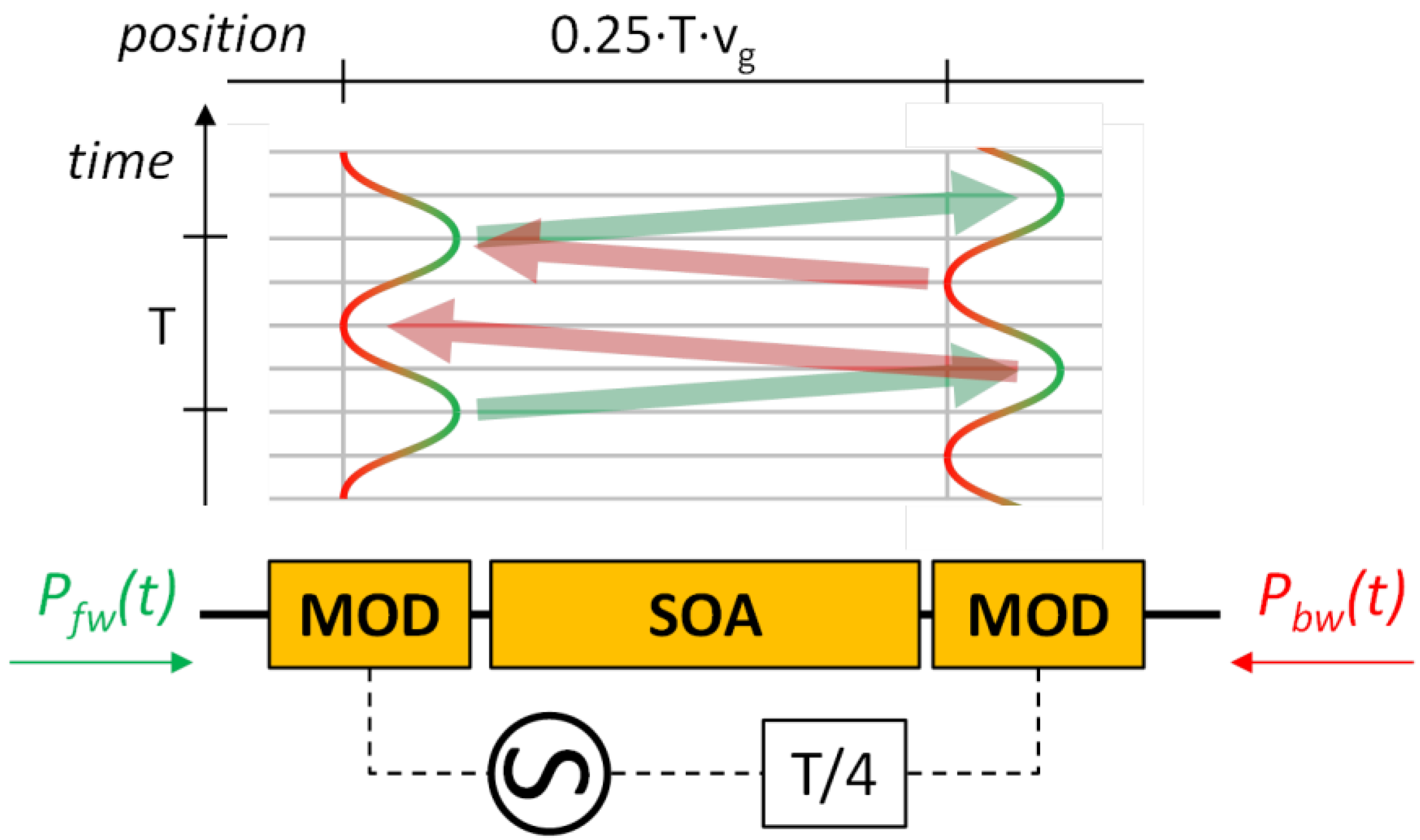
The concept for an MWP isolator is shown in
Figure 1, using two modulators. The modulators are driven with a period
T, by varying the voltage over them, and, hence, have a time-dependent transmission. A forward propagating oscillating signal in phase with the transmission modulation of the modulators will experience minimum loss. This figure shows clearly how a backward propagating signal will always encounter at least one modulator in a (partially) blocking state, if the distance between the two modulators corresponds to 0.25·T·v
g, with v
g the group velocity of the signal in the system. This means that from the perspective of the backward propagating signal, the two modulator gates are always modulated out of phase with each other, whereas from the perspective of the forward propagating signal, these modulator gates are modulated in phase.
Figure 1.
Schematic of the microwave photonics (MWP) isolator concept using modulators (MODs), showing the concatenated MOD-semiconductor optical amplifier (SOA)-MOD array, with the forward propagating signal Pfw entering from the left and the backward propagating signal Pbw entering from the right. The MOD gates are driven with a T/4 time difference, with T the period of the RF signal. The MOD transmission is indicated schematically with the sinusoid, with period T, with red indicating low transmission and green indicating high transmission. The green and red arrows are following the time-position grid and show how a forward propagating signal (green arrow) can pass two open gates, whereas a backward propagating signal (red arrow) always encounters at least on (partially) closed gate. The optical amplifier (SOA) can be used to compensate for overall insertion losses.
Although this concept would work with any type of RF-driven modulator, we limit the discussion to reversely-biased semiconductor optical amplifier (SOA) sections, effectively creating AMs, as was done in [
12]. The main reason is the obvious compatibility with the amplifying SOA sections in a PIC, which allows for integration of the MWP isolator after the output of a laser and even into a laser cavity, as will be shown in
Section 4. As mentioned above, this is the main rationale for an integrated isolator. From a fabrication perspective, this means that no epitaxial regrowth or overgrowth steps are required, nor techniques like quantum-well intermixing. Experimentally, it was validated that the SOA transmission, more specifically the absorption, changes with applied reverse bias voltage, and hence, it is feasible to use it as an AM [
16]. Note that in this implementation, the operating wavelength is well below the bandgap wavelength of the AM, which is different from what is typically called an electro-absorption modulator (EAM), in which case the wavelength is close to the bandgap.
We can model the MWP isolator, as shown in
Figure 1, using SOA rate equations for the optical field
A(
z,t) and the carrier density
N(
z,t) inside the SOA as presented in, e.g., [
12,
17]:
with the gain
G(
z,t) expressed as a linearized dependency on the carrier density
N(
z,t):
Here, the optical field
A(
z,t) is expressed in [W
1/2],
P(
z,t) is the optical power in [W],
ε is the nonlinear gain compression (0.2 W
−1 for SOA, 0 for AM,
i.e., reverse bias),
αN is the linewidth enhancement factor (3 for SOA, 1 for AM),
αint = 20 cm
−1 the passive loss,
FSE(
z,t) a Langevin noise term representing spontaneous emission,
I the injection current,
q the elementary charge,
V the volume of the active area,
τ the carrier recovery time (300 ps for SOA, 5 ps for AM), Γ = 0.3 the confinement factor,
ħ is Planck’s constant,
ω the optical angular frequency,
σ the mode cross section,
aN the differential gain coefficient (3 × 10
−20 m
2 for SOA, 12 × 10
−20 m
2 for AM) and
Ntr the transparency carrier density (0.3 × 10
18 cm
−3 for SOA, 0.7 × 10
18 cm
−3 for AM). These parameters are representative for the indium phosphide technology and have been experimentally verified, e.g., [
13]. The absorption dependency of the AM on the bias voltage is modeled using a voltage-dependent transparency carrier density
Ntr =
Ntr(
V(
t)), as proposed in [
18] and experimentally verified in [
13]. These equations are numerically solved using a spatial resolution of Δ
z = 5 µm, corresponding to a time resolution of Δ
t = 60 fs.
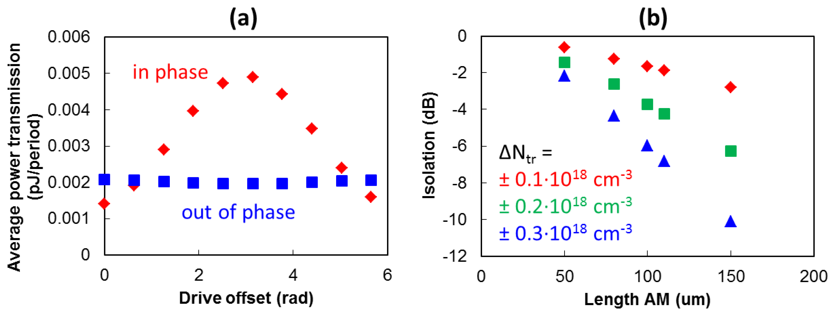
Using this model, the feasibility of the MWP isolator can be explored. The transmission of the forward and backward propagating 20-GHz MWP fields for an isolator with 100 µm-long AMs is shown in
Figure 2a. Obviously, the AM driving voltage needs to be in phase with the MWP signal oscillator for maximum transmission, as shown by the maximum around three radians drive offset. Note that this is a matter of calibrating the model, or any real-world system, and represents a relative value only. Since a system integrated on a PIC has known path lengths, the required drive offset is known beforehand. On the other hand, the counter-propagating signal has in practice an unknown phase with respect to the AMs, as reflections can originate from anywhere downstream of the circuit. However, as can be seen in
Figure 2a, this transmission is flat and below the peak transmission of the forward signal, indicating the isolation capability. Note that this flat transmission also means that isolation from continuous-wave counter-propagating signals is achieved.
In
Figure 2b, the isolation is plotted for various AM lengths and various driving voltage amplitudes of 3–9 V (corresponding to
Ntr = (0.1–0.3) × 10
18 cm
−3; [
13]). As can be expected, isolation increases with AM length and driving voltage amplitude. However, it has to be noted that such driving voltages are quite high, requiring between 100 mW and 1 W of RF power on the AM, assuming a 50-Ω termination. Based on these results, it can be seen that modest optical isolation ratios up to 10 dB can be achieved, which corresponds to close to a 20-dB microwave isolation, as most of the power is in the 20-GHz microwave fundamental harmonic, with up to 20% in the 40-GHz harmonic, due to the nonlinear transmission.
Figure 2.
(
a) Power transmission of a 1-mW peak power 20-GHz MWP signal through an isolator with a total length of 1.2 mm and with two absorption modulator (AM) sections of 100 µm. The bias amplitude corresponds to ±0.2 × 10
18 cm
−3. Referring to
Figure 1, the forward transmission (red) and reverse, backward transmission (blue) are shown, as a function of the phase difference between the MWP signal and the AM driving voltage. (
b) Maximum difference between forward and backward propagating signals for various AM lengths and driving voltages (indicated with
Ntr).
3. Experimental Realization in Hybrid Silicon Technology
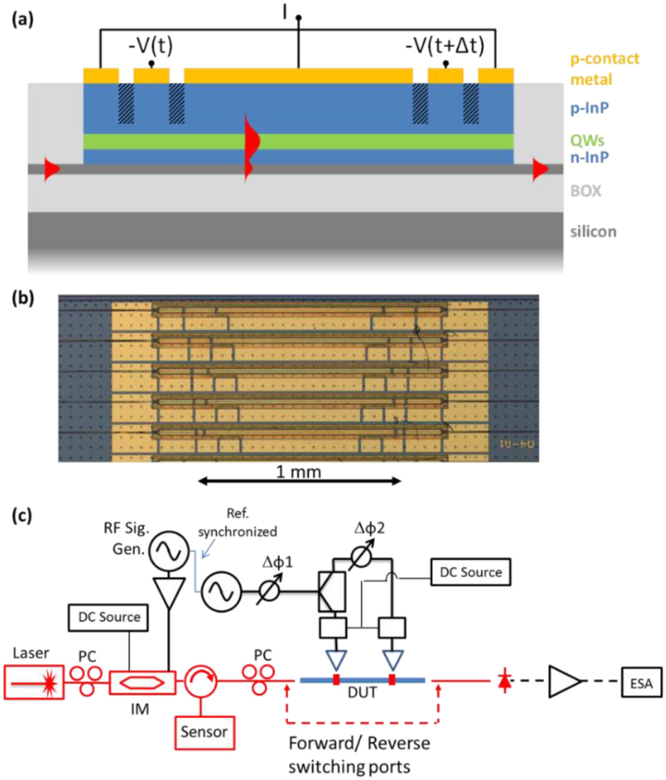
The MWP isolator was fabricated in the hybrid silicon platform [
19]. In this platform, an indium phosphide layer is bonded to a processed silicon photonic chip and then processed further, ensuring lithographic alignment accuracy. Silicon photonic components, such as waveguides, splitters and multiplexers, can be combined in this platform with hybrid waveguides, where the optical mode overlaps with the indium phosphide layers. In this way, active optical functionalities, such as gain, can be achieved. A schematic of the device cross-section is shown in
Figure 3a, where it can be seen that the optical mode propagates through an AM-SOA-AM sequence. The tapered mode converters from the silicon waveguide to the hybrid waveguide are electrically pumped, hence the small SOA sections at the start and end of the device [
20]. For details about the fabrication process, we refer to [
16]. The chip is diced, polished and anti-reflection coated for characterization.
The experimental setup to characterize the MWP isolator is shown in
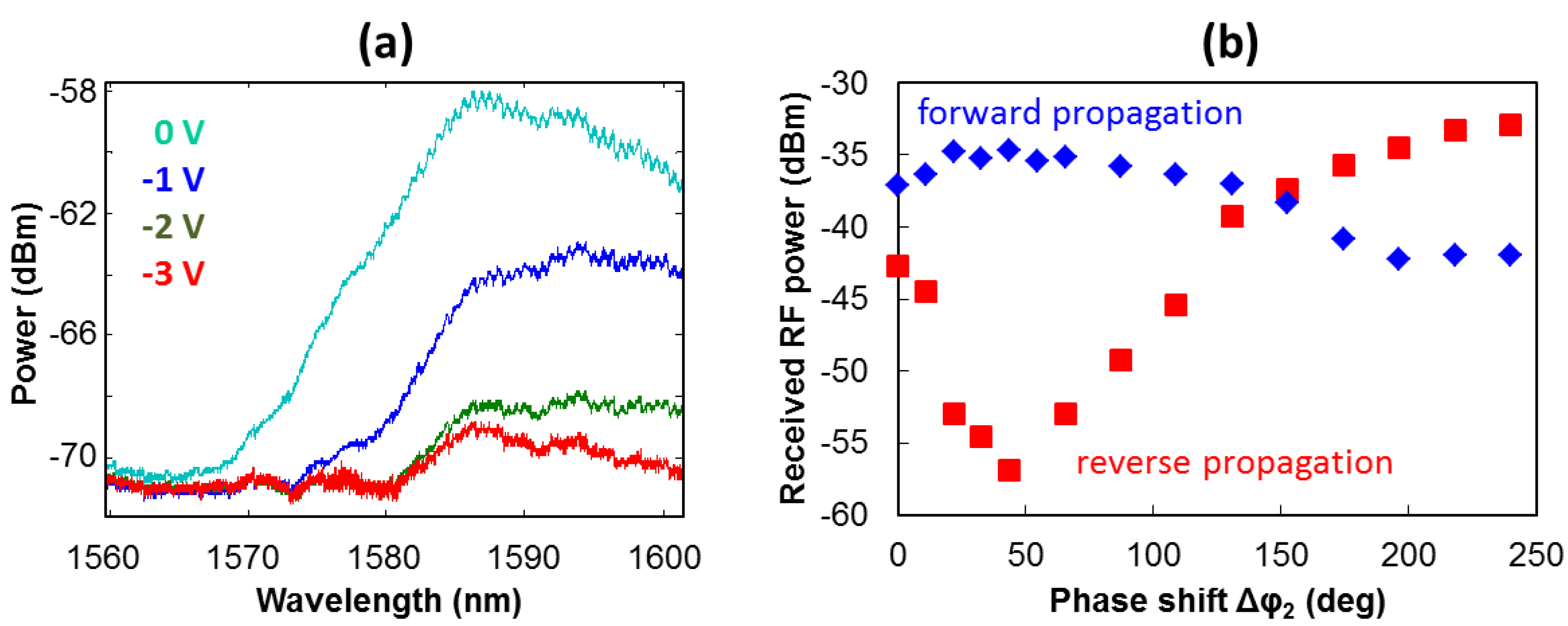
Figure 3c. An MWP signal is generated by an oscillator that is synchronized with the AM drivers. Two microwave phase shifters allow for independent tuning of the phase of the driving voltage on the AMs, compared to the MWP signal. The optical carrier wavelength is 1583 nm, as the AM has maximum dynamic range here, expressed as absorption change as a function of applied voltage. This was determined by looking at the amplified spontaneous emission spectrum of the SOA through the AM, on which the bias was varied, as shown in
Figure 4a. The MWP isolator insertion loss is 4.4 ± 0.5 dB, which of course depends on the SOA bias, in this case 200 mA. The overall active device length is 1.4 mm, with two 100-µm long AMs, positioned with a 1.0-mm spacing.
Figure 3.
(a) Schematic of the hybrid silicon MWP isolator, showing the optical field (red) as it propagates through the silicon waveguide, hybrid silicon III/V waveguide and the silicon waveguide again. Hydrogen-implantation of the p-doped InP cladding provides electrical isolation between the forward-biased SOA and the reverse-biased AM. N-contacts are to the side and not shown in this cross-section. (b) Microscope picture of an array of realized devices. (c) Experimental setup, showing the MWP signal generation using an intensity modulator (IM, Vπ = 3.6 V), driven by a signal generator (RF Sig. Gen.). This signal generator is synchronized with another signal generator that drives the two AMs. Two microwave phase shifters (Δφ1,2) are used to control the phase. The signal is recorded using an electrical spectrum analyzer (ESA) connected to a 40-GHz bandwidth photodiode and a 20-dB RF amplifier. Polarization controllers (PCs) are used to ensure transverse-electric polarization of the field inside the device under test (DUT). Lensed fibers are used to couple the light in and out of the device. Electrical connections are shown in black, optical connections in red. An estimated power of 12.5 dBm is used to drive each of the AMs. The SOA is biased at 200 mA. The circulator with the sensor is used for fiber to chip alignment.
![Photonics 02 00957 g003]()
Figure 4b shows the 20-GHz MWP signal transmission with Δ
φ1 set to drive one AM in phase with the MWP signal, while tuning the phase of the voltage on the other AM by Δ
φ2 (
Figure 3b). As can be seen, the received RF power varies with changing the phase on the second AM. Using this plot as a calibration, it can be seen that at Δ
φ2 = 50° ± 10°, the two AMs are driven at Δ
T =
T/4, as explained in
Figure 1, with
T = 50 ps. This means maximum transmission for the forward signal and minimum transmission for the counter-propagating signal. At Δ
φ2 = 230° ± 10°, this situation is reversed, as expected, and represents Δ
T = −
T/4. From this plot, it can be seen that 22-dB and 9-dB microwave isolations have been achieved, which agrees well with the optical isolation ratios up to 10 dB, obtained using our simulation. This comparison should be considered qualitative, as a complete set of SOA and AM parameters for the hybrid silicon platform is not available, and the simulation used parameters from the monolithic indium phosphide technology. However, since the active part of the hybrid waveguide is indium phosphide and since the simulation tool uses parameter values experimentally obtained with an indium phosphide SOA, it can be assumed that these outcomes should be close.
We note that ideally, the operation of the device should be symmetric for forward and reverse propagation. From
Figure 4b, it can be seen that this is not the case in the experiments. We hypothesize that due to processing non-uniformities, most notably variations in contact resistance over the length of the device, the AMs do not operate identically. In the linear regime, that would still not matter, but as the AM and SOA are nonlinear devices,
i.e., their transmission is power dependent, a difference between the two AMs would lead to a difference between the forward and reverse signals, even when both AMs are driven in phase.
Figure 4.
(a) Amplified spontaneous emission spectra, obtained by biasing the SOA with a constant current and measured after propagation through an AM. Bias voltage on the AM is varied from 0–3 V. (b) The RF power measured with the electrical spectrum analyzer for the forward and backward propagating MWP signals as a function of the phase difference between the two AM drive voltages.
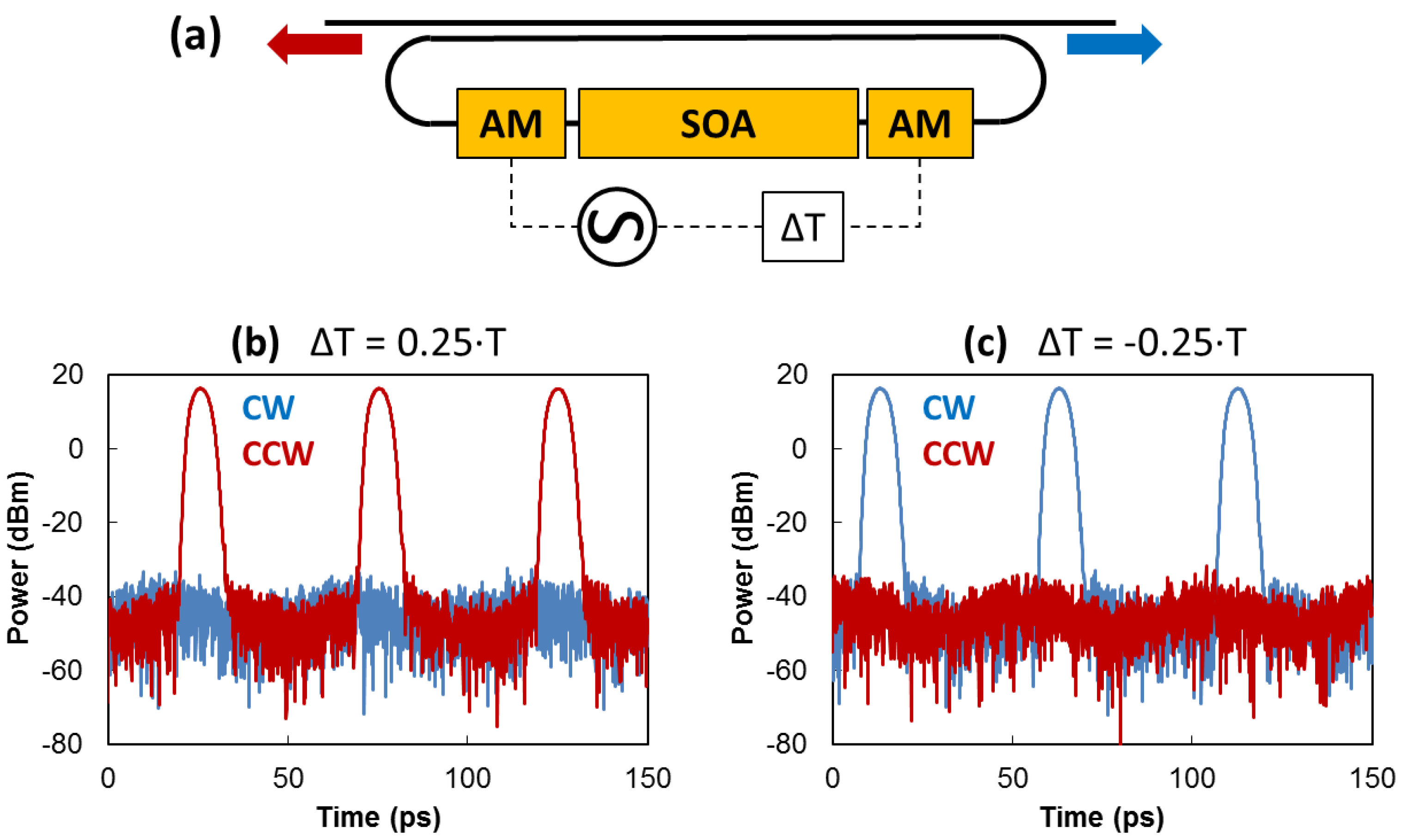
4. Application of the MWP Isolator in Unidirectional Ring Mode-Locked Lasers
The theoretical and experimental results show clearly the potential for isolation, though with a somewhat limited extinction ratio up to ~10 dB optical and ~20 dB electrical. One possible application could be to use this MWP isolator inside a ring laser cavity. It is well known that a small periodic variation in the gain can cause mode-locking,
i.e., the laser operates in a pulsed mode [
21]. Such MLLs have been realized in various configurations, but ring lasers are particularly attractive due to the lack of mirrors and, hence, the ease of integration on a PIC. However, such ring MLLs are intrinsically bi-directional [
18], which leads to lower output efficiency and higher amplitude and phase noise due to cross-gain modulation. It has been shown theoretically and experimentally that by careful MLL cavity design, the power ratio in two counter propagating fields can be controlled, however only to a limited extent [
22,
23].
In this section, we explore theoretically the feasibility of using the MWP isolator to force the MLL into a unidirectional regime. We use the model presented above (Equations (1)–(3)), extended with a 5-THz SOA gain bandwidth filter, to limit the pulse shortening. The model is implemented using a similar approach as in [
19].
Figure 5a shows the layout of a ring MLL with a dual AM-phased drive, which means that the MLL is effectively hybridly mode-locked, as the AMs are saturable absorbers and this saturation contributes to the pulse shaping mechanism. The length of the ring determines the period
T of the output pulses, and the AMs are placed with a separation corresponding to
T/4.
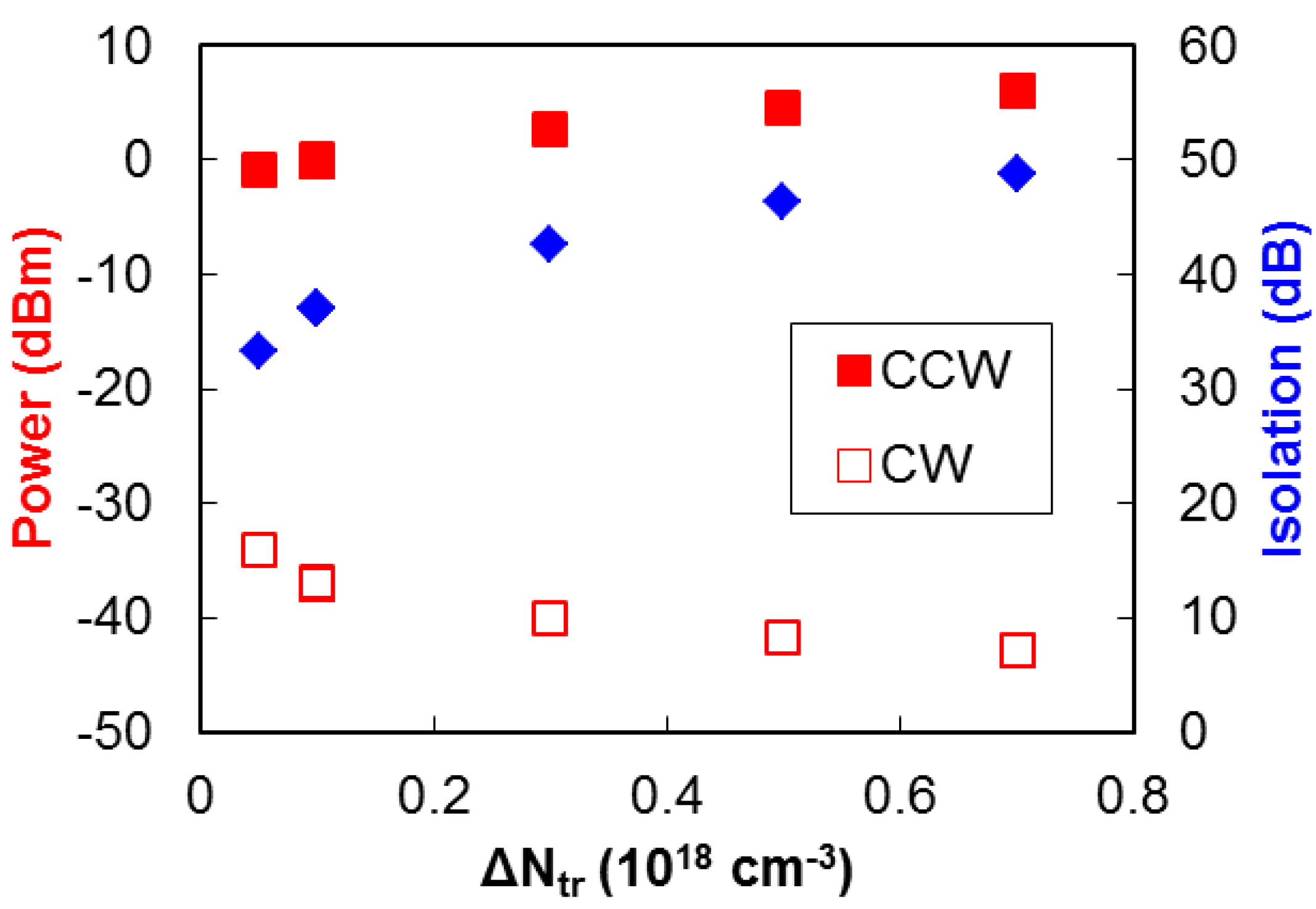
Figure 5b,c shows the simulated clockwise (CW) and counter-clockwise (CCW) optical output fields for a 20-GHz ring MLL and with an AM drive delay of 12.5 ps and −12.5 ps, respectively. As can be seen, the ring MLL operates unidirectionally with the correct phase of the drive voltage on the AMs. The isolation or suppression of the counter propagating field depends on the MLL operating conditions. In
Figure 6, this is shown for a MLL with varying drive voltage amplitude, here again expressed by varying the amplitude of the oscillation of the transparency carrier density
Ntr. The suppression of the counter propagating field ranges from 30 dB–50 dB, for increasing drive voltage amplitude.
Figure 5.
(a) Schematic layout of the unidirectional mode-locked laser (MLL), showing an oscillator driving the two AMs, with a relative delay of ΔT. A directional coupler couples light out of the ring into the clockwise (CW, blue) or counterclockwise (CCW, red) output waveguide. The simulated output of a 20-GHz MLL is shown for (b) ΔT = 12.5 ps and (c) ΔT = −12.5 ps. The SOA length is 800 µm, and the AMs have a length of 25 µm. Power output coupling is 0.5 per roundtrip. The simulation parameters are ΔNtr = 0.7 × 1018 cm−3 and ISOA = 80 mA.
Figure 6.
Average output power for the clockwise (CW) and counter-clockwise (CCW) signals, assuming Δ
T = 12.5 ps in
Figure 5a, as a function of the modulation amplitude Δ
Ntr of
Ntr. The isolation ratio is also shown (blue). The SOA injection current is 80 mA. Further MLL design parameters are as in
Figure 5.
In conclusion, we have shown the feasibility of an integrated unidirectional ring MLL, using our experimentally-verified concept of an MWP isolator. Apart from a more efficient output, the lack of cross-gain modulation and spatial hole burning will likely lead to lower phase and amplitude noise. Furthermore, it can be hypothesized that the laser is less sensitive to optical feedback, as this feedback is injected in the suppressed counter propagating mode. Major applications can be foreseen in on-chip low noise microwave generation and in on-chip comb generation for wavelength-division multiplexed systems.
5. Conclusion and Outlook
In this paper, we have presented the concept of a novel integrated MWP isolator and its first experimental realization in the hybrid silicon platform. Optical and microwave isolation ratios were simulated to be in the range up to 10 dB and 20 dB, respectively, using parameters representative for the indium phosphide platform. The experimental realization of this device in the hybrid silicon platform showed microwave isolation in the 9 dB–22 dB range.
Such isolation ratios are barely sufficient for on-chip use, for example to shield a laser from optical feedback. As was argued in [
24], optical isolation of at least 20 dB is required. Options to enhance the MWP isolator include the concatenation of more AM gates and using more square-shaped driving pulses, which would also reduce higher harmonic generation.
In an alternative implementation, when using this MWP isolator inside a resonant cavity, the isolating effect is strongly enhanced. We have presented a design study on the use of MWP isolators inside a ring MLL cavity. Simulations show that unidirectional operation can be achieved, with a 30–50-dB suppression of the counter propagating mode, at limited driving voltages. The potentially low noise and feedback-insensitive operation of such a laser makes it a very promising candidate for use as on-chip microwave or comb generators.
The simulations were based on the indium phosphide material system, and an implementation using reversely-biased SOA sections or AMs was chosen. This choice offers a practical path to integration with (forward biased) SOAs, for example to realize the unidirectional ring MLLs that were presented in this work. Alternative approaches for the AMs can include Mach–Zehnder interferometer modulators in the silicon photonics platform, electro-absorption modulators in the indium phosphide and hybrid silicon platforms or even forward-biased SOAs as gates. The choice will depend on all trade-offs that are required for PIC design and fabrication. Choosing modulators with a higher extinction ratio will improve the isolation ratio. Another important aspect is the optical bandwidth that is required. Mach–Zehnder interferometer modulators and forward-based SOAs are broadband, having bandwidths of at least tens of nanometers. Electro-absorption modulators and reversely-biased SOAs have a very wavelength-dependent transmission and are hence narrow band, typically only a few nanometer, e.g., as shown in [
25] and in
Figure 4.
The experimental realization on the hybrid silicon platform is a relevant step, as this platform has been shown to have interesting applications in the field of MWP [
26]. Although one can argue that similar PIC functionalities can be achieved using a monolithic indium phosphide platform, the hybrid silicon platform offers the potential of economies of scale, in terms of fabrication on 6” or even 8” substrate wafers and the compatibility with the mature CMOS manufacturing infrastructure. This also includes the required integration with electronic driving and control circuitry, which can be done in a package [
27] or fully monolithically on the same chip [
28]. Such an approach is necessary for large volume applications that can be envisioned for MWP, which include, for example, 5G wireless communications infrastructure.


