Article

Long-Wavelength InAs/GaAs Quantum-Dot Light Emitting Sources Monolithically Grown on Si Substrate

1
Department of Electronic and Electrical Engineering, University College London, London WC1E 7JE, UK
2
Institute for Nanoscience and Engineering, University of Arkansas, Fayetteville, AR 72701, USA
*
Author to whom correspondence should be addressed.
Photonics 2015, 2(2), 646-658; https://doi.org/10.3390/photonics2020646
Submission received: 29 May 2015 / Revised: 14 June 2015 / Accepted: 15 June 2015 / Published: 18 June 2015
(This article belongs to the Special Issue Quantum Dot Based Lasers and Photonic Devices)

Abstract

:
Direct integration of III–V light emitting sources on Si substrates has attracted significant interest for addressing the growing limitations for Si-based electronics and allowing the realization of complex optoelectronics circuits. However, the high density of threading dislocations introduced by large lattice mismatch and incompatible thermal expansion coefficient between III–V materials and Si substrates have fundamentally limited monolithic epitaxy of III–V devices on Si substrates. Here, by using the InAlAs/GaAs strained layer superlattices (SLSs) as dislocation filter layers (DFLs) to reduce the density of threading dislocations. We firstly demonstrate a Si-based 1.3 µm InAs/GaAs quantum dot (QD) laser that lases up to 111 °C, with a low threshold current density of 200 A/cm2 and high output power over 100 mW at room temperature. We then demonstrate the operation of InAs/GaAs QD superluminescent light emitting diodes (SLDs) monolithically grown on Si substrates. The fabricated two-section SLD exhibits a 3 dB linewidth of 114 nm, centered at ~1255 nm with a corresponding output power of 2.6 mW at room temperature. Our work complements hybrid integration using wafer bonding and represents a significant milestone for direct monolithic integration of III–V light emitters on Si substrates.

1. Introduction

Silicon, one of the most important semiconductor materials, offer not only fantastic electronic and mechanical properties, but is also abundant, low-cost, and toxic-free. Although it has been the mainstays for modern electronics, it is not widely used for light emitting sources because bulk silicon is an inefficient emitter, a result of indirect bandgap. In contrast, III-V compound semiconductors, such as GaAs and InP, have a direct bandgap and hence have high light emission efficiency. However, such materials are more expensive than silicon. Therefore, the growth of III-V light emitters on Si substrates to combine the advantages of both has recently stimulated enormous scientific interest for applications ranging from chip-to-chip, system-to-system optical interconnectors and telecommunications [1]. Still another benefit of integrating GaAs and InP on Si substrates is for taking advantage of the comparably higher thermal conductivity of Si to improve the heat sinking of GaAs and InP devices. Apparently then, the capacity to fabricate high quality III-V’s, typically GaAs, on Si substrates is the “holy grail” worth grasping.
So far, the direct epitaxial growth of III-V’s on Si substrates has been regarded as one of the most promising options to realize high performance light sources on Si substrates. This technique, however, suffers from a number of roadblocks. The most severe problem has been the formation of high density threading dislocations between GaAs and Si due to large thermal and lattice mismatches. This is absolutely troubling since any threading dislocations propagating into the active media will become non-radiative recombination centers, reducing minority-carrier lifetime, and hence deteriorate device performance. To achieve high crystal quality and reduce the density of dislocations, several methods have been proposed, including thermal annealing [2], two-step low temperature growth [3], the use of a titled Si substrates [4], growth of a nucleation layer [5,6] and growth of a strained layer superlattice (SLS) buffer [7,8,9,10].
Most recently, III-V quantum-dot (QD) based light emitters, especially QD lasers, have been considered to be the most attractive candidate for realizing practical III-V/Si lasers owning to their unique characteristics, in particular ultra-low threshold currents [11], temperature insensitivity and less sensitivity to threading dislocations, hence impressive results have been achieved [5,8,12,13,14,15,16,17,18]. In addition to QD lasers, QD-based superluminescent light emitting diodes (SLDs) have also experienced rapid development for applications in many areas, such as fiber-optic gyroscopes [19], optical coherence tomography (OCT) [20] and wavelength-division multiplexing systems [21], because they benefit significantly from QD’s inherently large size inhomogeneity when grown by the Stranski–Krastanow (S-K) mode [22].
In this paper, we introduce InAlAs/GaAs SLSs as dislocation filter layers (DFLs) for reducing the density of threading dislocations. Based on this technique, we show that a Si-based laser can achieve lasing up to 111 °C with a threshold current density of 200 A/cm2 and high output power of 101 mW at room temperature. We then describe the operation of III-V QD SLD on Si substrates producing a broad linewidth of 114 nm at ~1255 nm with a corresponding output power of 2.6 mw at room temperature.

2. Quantum Dot Lasers on Si Substrates

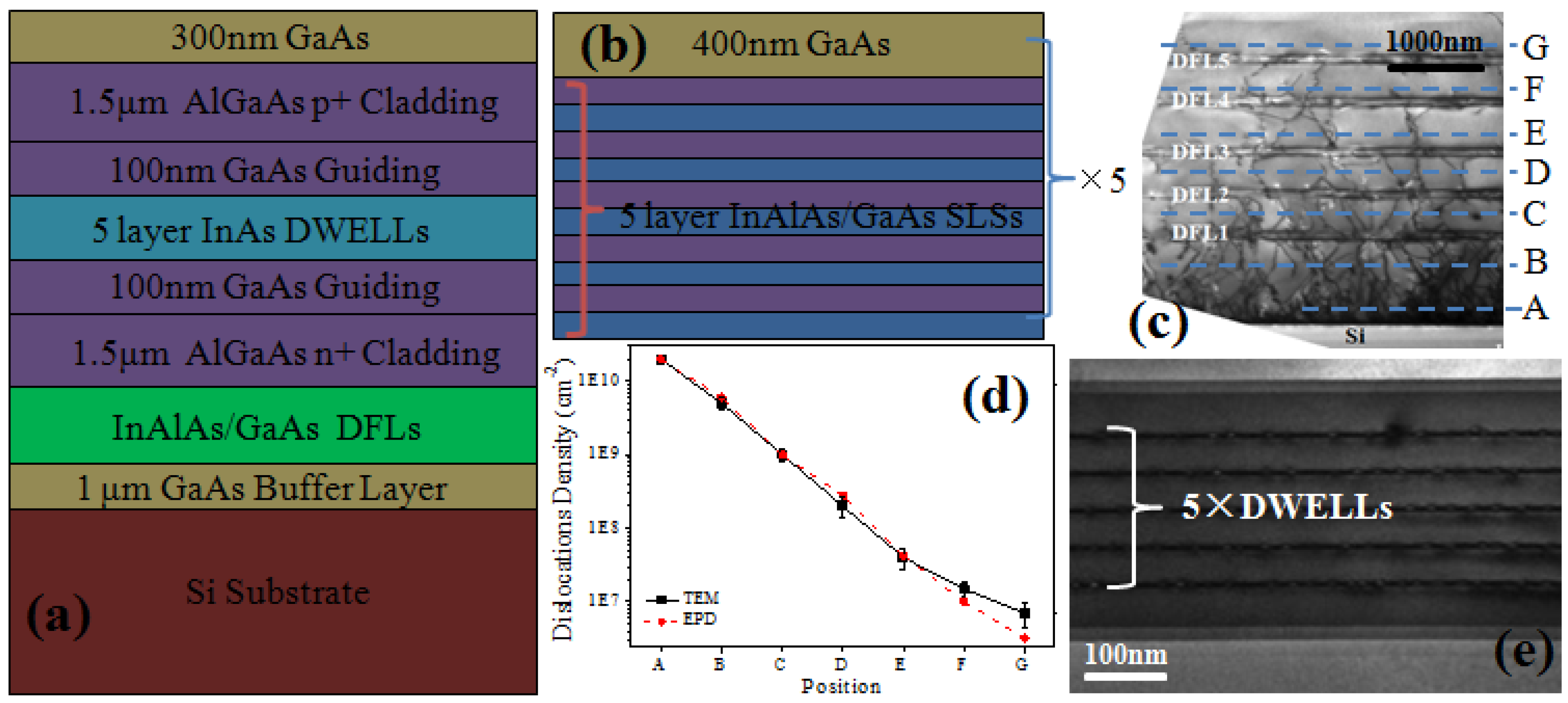
2.1. MBE Growth and Effect of InAlAs/GaAs SLSs on the Quality of III-V Material Grown on Si Substrates

The Si-based QD laser structure was grown on a phosphorus-doped Si (100) substrate with 4° offcut toward the [110] plane in a solid-source III–V molecular beam epitaxy (MBE) system. Oxide desorption was accomplished by holding the Si substrate at a temperature of 900 °C for 10 min. Epitaxy was then performed in the following orders as shown schematically in Figure 1a. The initial 30 nm nucleation layer was grown at 400 °C with a low growth rate of 0.1 monolayer (ML)/s, while the remaining 970 nm buffer layer was grown at an elevated temperature with a high growth rate of 0.7 ML/s. The use of such an optimized two-step growth scheme has been demonstrated to effectively confine threading dislocations [3]. Above GaAs buffer layer, a series of InAlAs/GaAs dislocation filter layers were grown, followed by a 1.5 µm n-doped AlGaAs lower cladding layer. After a 100 nm GaAs waveguide layer, a typical five-layer InAs/InGaAs/GaAs dot-in-well (DWELL) [23] layers were grown at around 510 °C. Each DWELL layer was formed by deposited 3 ML/s of InAs embedded between a 2 nm InGaAs and 6 nm InGaAs layer. The five layers of DWELL structure were each separated by 45 nm undoped GaAs barrier layer. Above the undoped active region is grown a second 100 nm GaAs waveguide layer, followed by a 1.5 µm p-doped AlGaAs upper cladding layer, and finally a 300 nm-thick highly doped GaAs contacting layer.
Figure 1. (a) Schematic of the layer structure. (b) Schematic of the InAlAs/GaAs dislocation filter layers (DFLs). (c) Cross-sectional TEM image of InAlAs/GaAs DFLs. (d) Changes in dislocation density, determined by TEM and etch-pit defects (EPD), counted at different positions labeled in Figure 1c. (e) Cross-sectional TEM image of the active region.
Photonics 02 00646 g001
The epitaxial structure of InAlAs/GaAs DFLs is schematically shown in Figure 1b. This design consists of five repeats of five-period of InAlAs (10 nm)/GaAs (10 nm) SLSs and 400 nm GaAs spacing layer. To study the effect of InAlAs/GaAs SLSs serving as DFLs, transmission electron microscopy (TEM) measurements were carried out as shown in Figure 1c, and the reduction of dislocation density governed by DFLs, obtained by TEM and etch-pit defects (EPDs), is summarized in Figure 1d. Due to the large lattice mismatch between GaAs and Si substrate, an extremely high density (~1.5 × 1010 cm−2 counted at position A) of threading dislocations is created at the GaAs/Si interface. Note that most (more than 60%) of the defects are confined within the first 200 nm buffer layer; this is attributed to the optimized two-step low temperature growth. However, still a high density of threading dislocations has been ‘escaped’ propagating towards the active region. Five-set of DFLs, in this case, are utilized to eliminate these threading dislocations. As seen, before the DFL1, the density of threading dislocations is estimated to be ~5 × 109 cm−2 (counted at position B), while, after the DFL1, the density of threading dislocations has been reduced to ~1 × 109 cm−2 (counted at position C), with its defects density further reduced after the DFL2 to ~3 × 108 cm−2 (counted at position D). These observations indicate that, owing to the misfit strain that arises from adjacent layers, InAlAs/GaAs DFLs can effectively suppress/block the propagation of the threading dislocations by bending/redirecting the threading dislocations away from the growth plane [24,25]. And after the last set of DFL, i.e., DFL5, the average threading dislocation density has been significantly reduced to ~5 × 106 cm−2 (counted at position G). Figure 1e presents a cross-sectional TEM image of the active region of InAs/GaAs QDs grown on Si substrate using InAlAs/GaAs DFLs, and it is clear to see that no obvious dislocations can be observed.
Figure 2. (a) AFM image of InAs quantum dots (QDs) grown on Si substrates. (b) Cross-sectional TEM image of one InAs QD. (c) Normalized photoluminescent (PL) room temperature (RT) emission spectra of InAs/GaAs QDs grown on Si substrate and GaAs substrate with the same growth conditions.
Photonics 02 00646 g002
Atomic force microscopy (AFM), cross-sectional TEM and photoluminescent (PL) measurements were also carried out to characterize the structure and optical properties of InAs/GaAs QD laser structure directly grown on Si substrate using InAlAs/GaAs DFLs as shown in Figure 2. The dot density, as measured by AFM (see Figure 2a), is estimated to be ~4 × 1010 cm−2. From TEM (see Figure 2b), the typical near-pyramidal dots are ~25 nm in base and ~7 nm in height. Figure 2c compares RT PL spectra of InAs/GaAs QDs grown on Si substrate and GaAs substrate under the same growth conditions. As seen, room temperature PL emission at round 1280 nm with full width at half maximum (FWHM) of ~36meV is obtained for InAs/GaAs QDs grown on Si substrate, which is similar to that of ~32meV for InAs/GaAs QDs grown on GaAs substrate. And of considerable significance is that the PL intensity of the InAs/GaAs QDs grown on Si substrate is comparable to the value obtained from InAs/GaAs QDs grown on GaAs substrate.

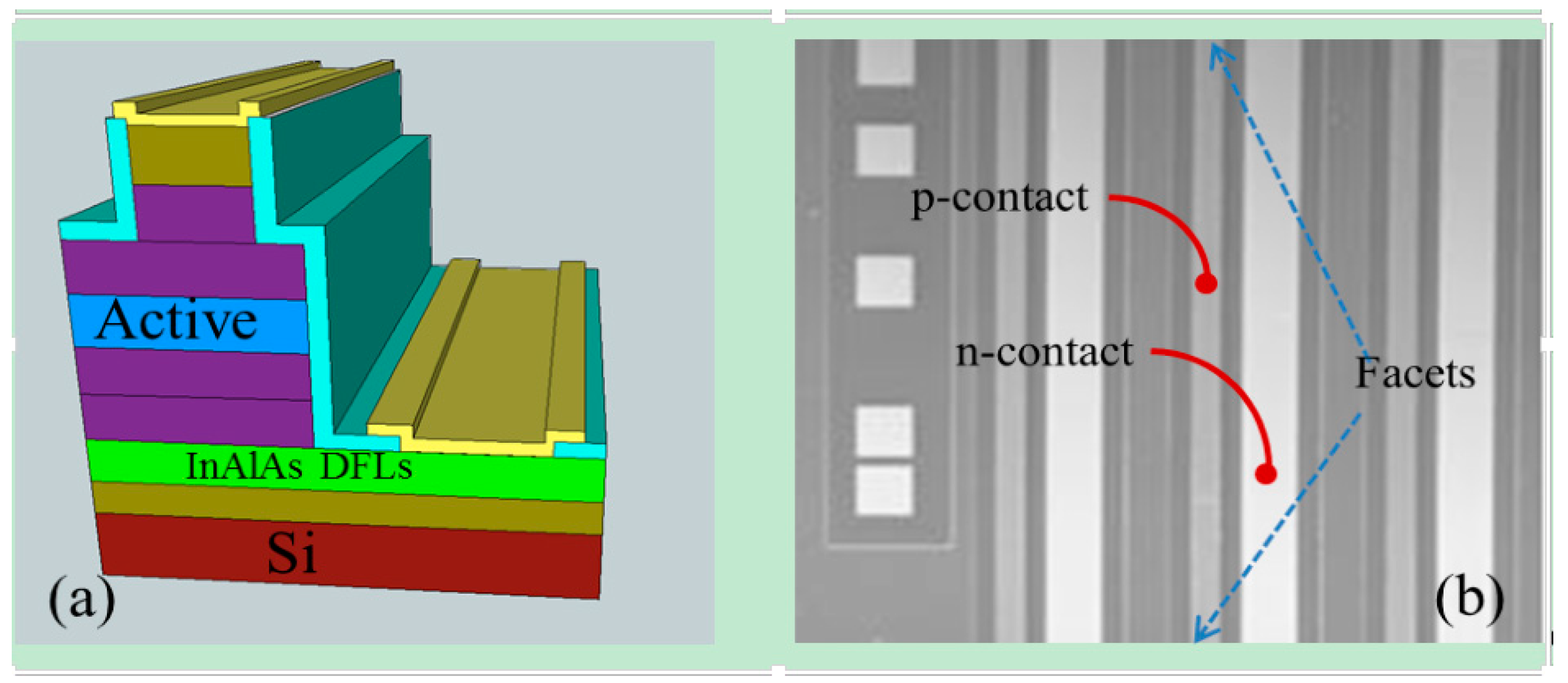
2.2. Device Fabrication of Si-Based Lasers

Broad-area lasers with either 25 or 50 µm wide stripes were fabricated following standard photo-lithography and wet etching techniques as shown schematically in Figure 3a. It should be mentioned that top N+ metal contacting layer was deposited on the exposed highly n-doped GaAs contacting layer, which was settled between N+ AlGaAs cladding layer and DFLs. Figure 3b shows the SEM imaging (top view) of the final devices described in this paper, which were 25 µm in width and 3 mm in length, and were processed with as-cleaved facets. No facet coating was applied. Devices were then mounted and wire bonded on AlN tiles to enable testing. Deice characterization was carried out, unless stated otherwise, under pulsed mode of 1% duty cycle and 1µs pulsed width to reduce the self-heating of the device.
Figure 3. (a) Schematic of the Si-based laser. (b) SEM image of the final laser devices (top view).
Photonics 02 00646 g003

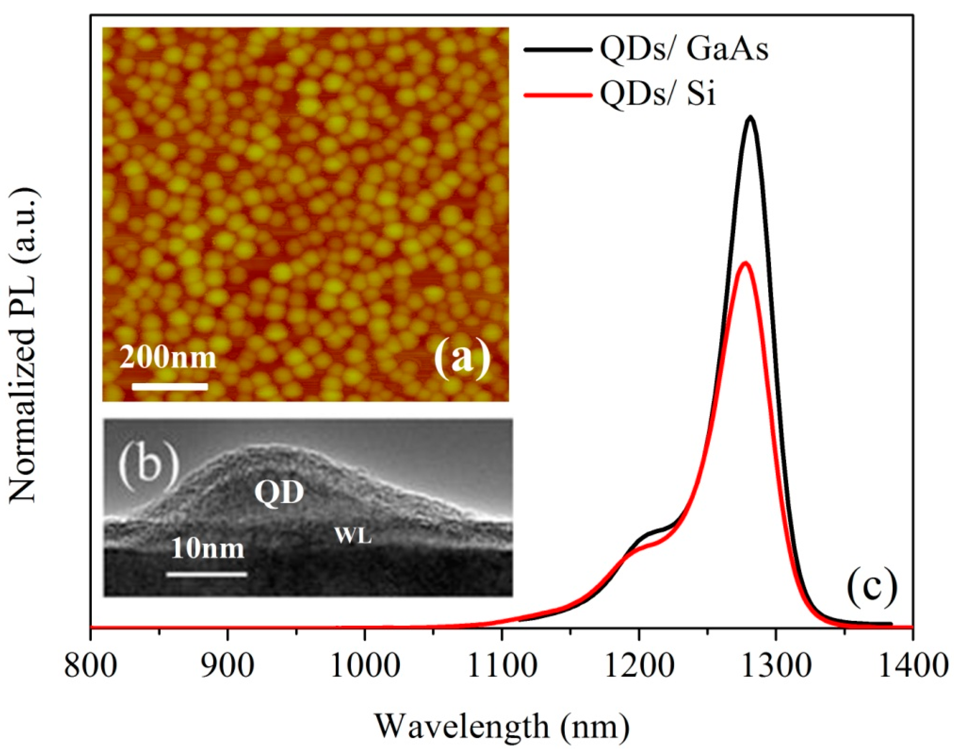
2.3. Results and Discussion

Figure 4 presents the evidence of lasing from an InAs/GaAs QD laser monolithically grown on Si substrate. Figure 4a shows the emission spectra from a Si-based laser at different injection current densities. At low injection of 100 A/cm2, the emission is broad with the full-width-half-maximum (FWHM) of 50 nm centered at ~1.3 µm. As the injection increases to 190 A/cm2, the peak broadens to 62 nm due to the state filling of the dots and increases in intensity, also, a shoulder emerging at ~1255 nm. As the current density increased to 210 A/cm2, the peak at ~1255 nm increases sharply in intensity and narrows to ~2.4 nm, which is an obvious evidence of lasing. Further increasing the injection current density to 400 A/cm2, a multi-mode lasing spectrum appears. Figure 4b shows the L-I curve of characteristics for InAs/GaAs QDs laser on Si substrate, in which a clear knee behavior in the L-I curve is observed at the lasing threshold of 200 A/cm2. Significantly, the single facet output power has been measured as high as 101 mW at an injection current density of 1.2 kA/cm2, with no evidence of power saturation up to this current density.
Figure 4. (a) Emission spectra at different injection current densities. (b) L-I curve of InAs QD laser on Si substrates.
Photonics 02 00646 g004
Figure 5. (a) L-I curve for InAs QD laser on Si at 111 ºC. (b) Lasing spectrum just above the threshold at 111 ºC. (c) Temperature dependence of the threshold current density under pulsed operation.
Photonics 02 00646 g005
Temperature-dependent L-I characteristics, ranging from 20 to 111 ºC, were also performed. Figure 5a shows the output power against the current density at 111 ºC, a threshold current density of ~1.28 kA/cm2 is obtained, which has been further evidenced by the lasing spectrum at the lasing threshold of 1.28 kA/cm2 as presented in Figure 5b. To the best of our knowledge, this is the first demonstration of an InAs/GaAs QDs laser directly grown on Si substrate that can lase over 100 ºC. A characteristics temperature (T0) was calculated from the temperature dependency of Jth, yielding a value of 50 K from 20–110 ºC. The value of T0 reported here is comparable to previous works on 1.3 µm InAs/GaAs QDs lasers on native GaAs substrates. This strong dependency of Jth on temperature is mainly due to the increased non-radiative recombination and carrier escape from the hetero-junctions at high temperature. In future devices, this relatively poor T0 can be improved by p-doping of the QDs [26,27].

3. Quantum Dot SLDs on Si Substrates

3.1. Experimental Procedure

The Si-based SLD structure was grown by solid-source III–V MBE reactor on a n-doped Si (100) substrate with 4° offcut toward the [110] plane. To reduce the density of threading dislocations introduced by large lattice mismatch and difference in thermal expansion coefficient of the two materials, five sets of InAlAs/GaAs DFLs, adopted in laser structure grown on Si substrate (as described in Section 2.1), have also been utilized here to optimize the buffer layer. As a result, a very low defect density is observed in the QDs active region of SLD structure grown on Si as shown in the cross-sectional TEM image (Figure 6a). The MBE growth of Si-based SLD structure is nominally identical to that of Si-based laser structure, except for the arrangement of the QDs active region. Here, in contract to the growth of QDs for laser structure [10], the growth conditions were intentionally offset from the optimized conditions, used during the formation of QDs with a high uniformity and a high density, in order to achieve a large size inhomogeneity [28], which aims to produce a broad spectrum bandwidth. AFM measurements were performed on uncapped InAs/GaAs QDs samples with the grown conditions optimized for lasers and SLDs. Figure 6c shows a typical AFM image for the sample with the grown conditions optimized for SLDs. As seen, compared to the AFM image of laser structure (see Figure 2a), a large size inhomogeneity of dots has been achieved, which has great advantages for realizing broad bandwidth. The normalized PL spectra for InAs/GaAs QDs samples optimized for lasers and SLDs at 77 K is shown in Figure 6c, it can be seen that the InAs QDs optimized for SLDs emit a PL emission of 84 nm much wider than that of grown for lasers, which has a PL bandwidth of 38 nm.
An InAs/GaAs QD SLD structure was developed on a Si substrate based on the basis of the optimized conditions for the buffer layer and the action region described above. The five-layer InAs DWELL active region was sandwiched by a p-doped upper cladding layer and n-doped lower cladding layer of 1.5 µm Al0.4Ga0.6As. And finally a 300 nm p-doped GaAs contact layer accomplished the SLD structure. Two-section ridge-waveguide SLDs with a ridge width of 20 µm were fabricated following standard photolithography, wet etching and metallization techniques [29]. Two sections were formed by shallow etch of the highly p-doped GaAs contacting layer, yielding a resistance of ~2 KΩ between adjacent contacts. Figure 6d shows the schematic of the two-section SLD. The device described in this paper consists of a 2 mm gain section operated under forward current injection and a 1 mm absorber, which was reversely biased to reduce the optical feedback, therefore inhibiting lasing action. The devices were processed with as-cleaved facets with no facet coating applied.
Figure 6. (a) Cross-sectional TEM image for the active region of the InAs QD grown on Si substrates. (b) AFM image of uncapped InAs QDs optimized for broad linewidth. (c) Normalized PL spectra of InAs QDs with the growth conditions optimized for laser structure and superluminescent light emitting diodes (SLD) structure at 77K. (d) Schematic of the two-section QD SLDs on Si substrates.
Photonics 02 00646 g006

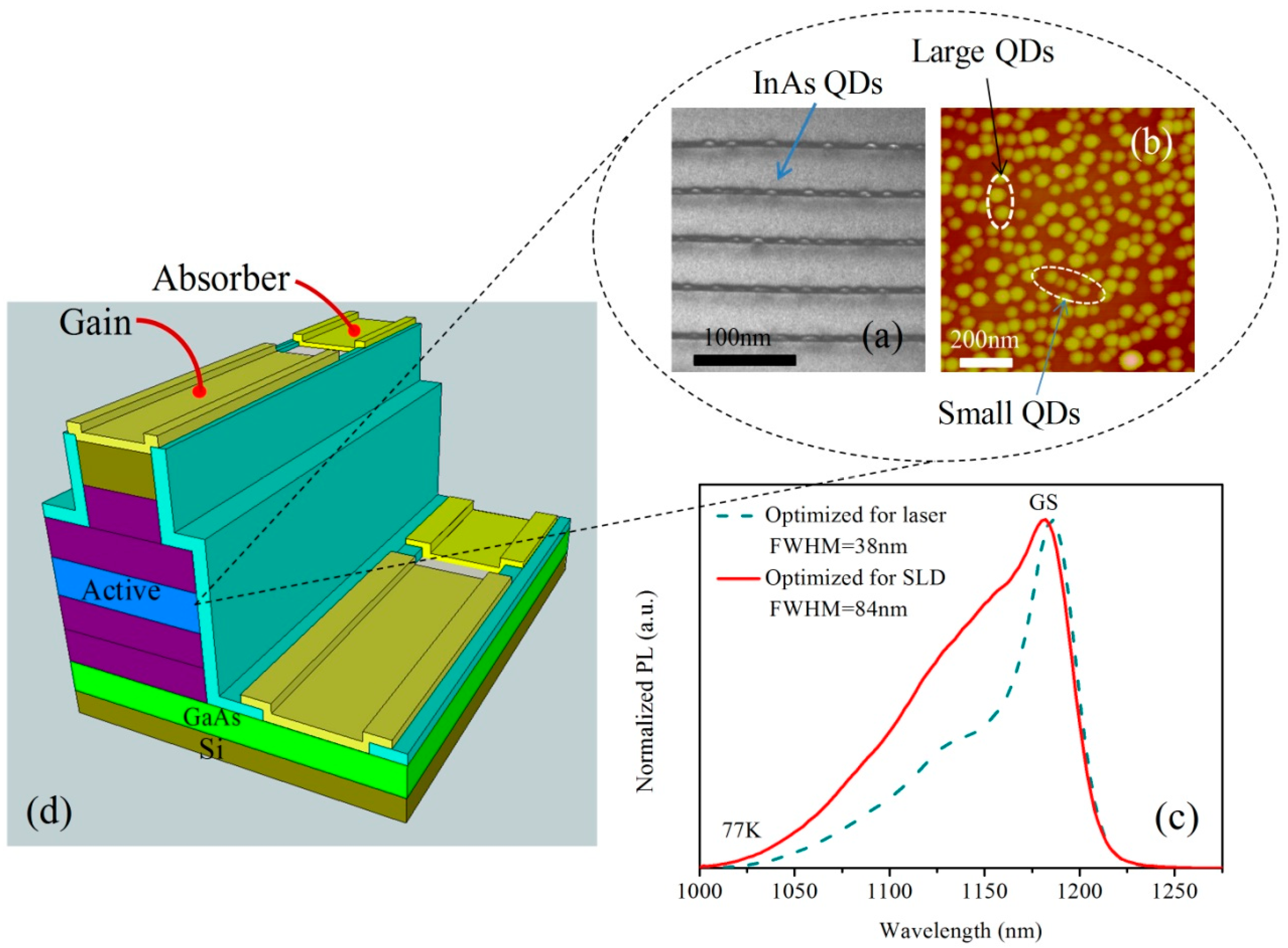
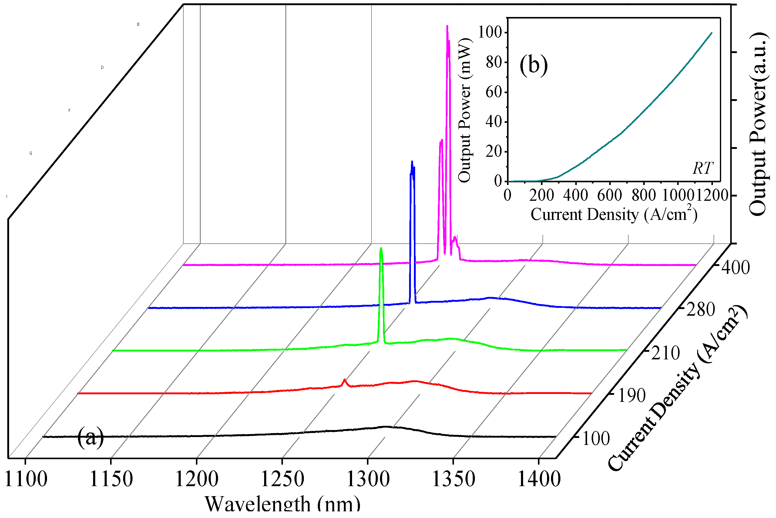
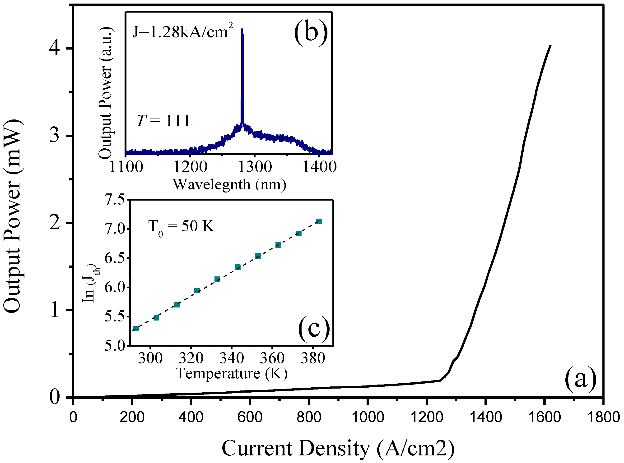
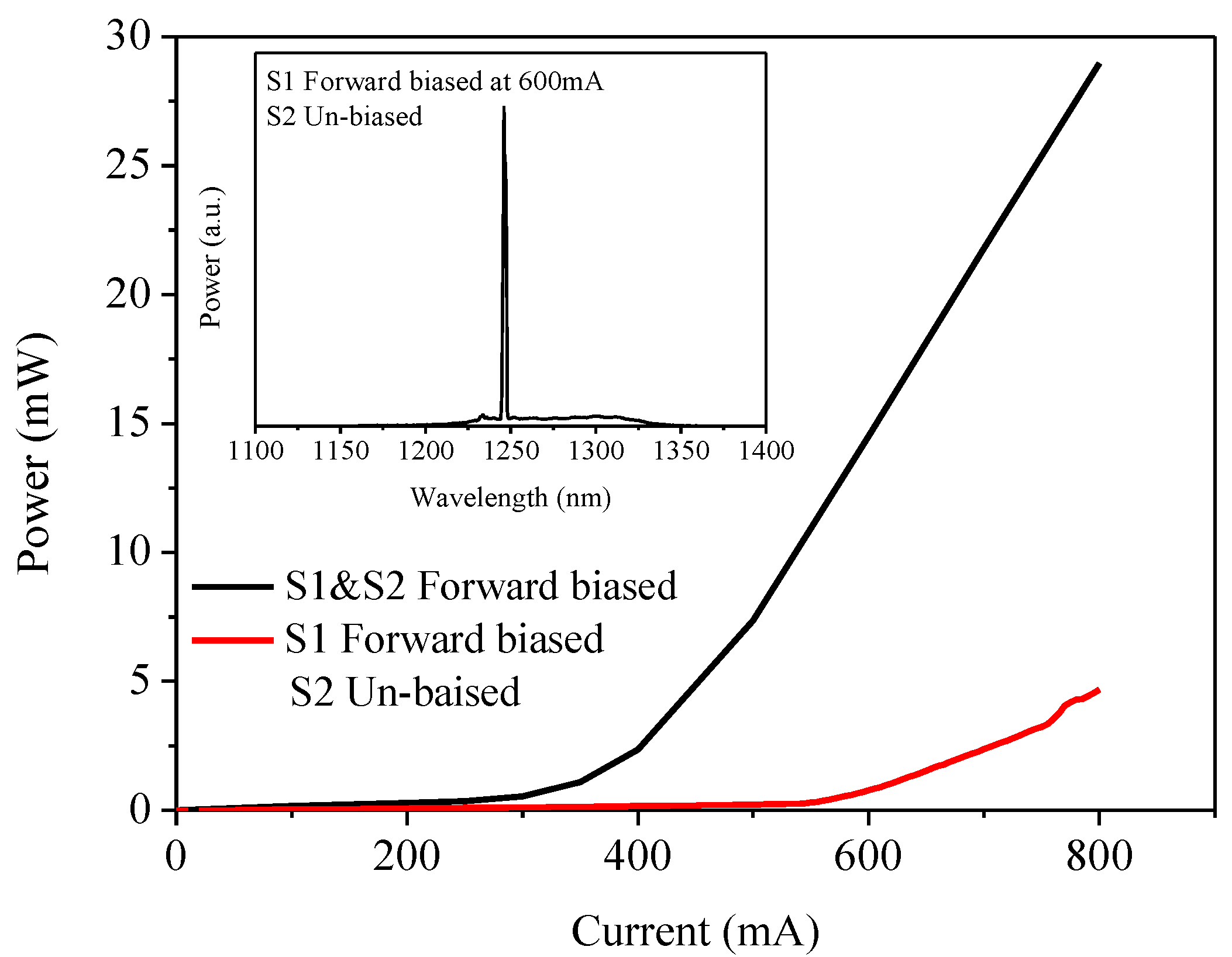
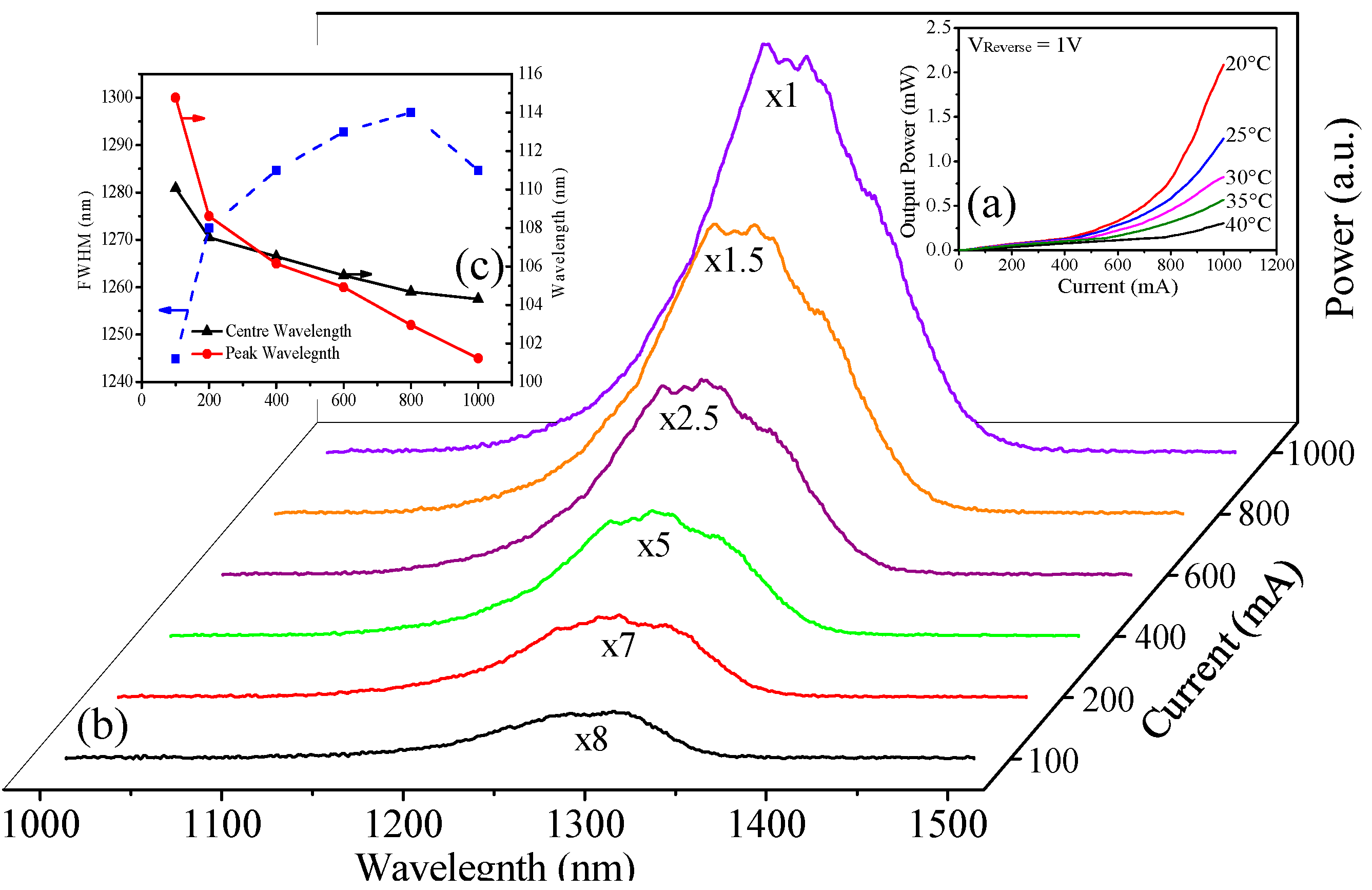
3.2. Results and Discussion

Figure 7a shows the L-I characteristics of the two-section InAs/GaAs QDs device grown on a Si substrate with different absorber biasing conditions. The measurements were carried out by electrically injecting the gain section (S1) under pulsed operation of 5% duty cycle and 10 µs pulse width to minimize the self-heating of the device, while with the absorption section (S2) either forward biased or un-biased. When both S1 and S2 are forward electrically pumped under the same pulsed conditions (5% duty cycle and 10 µs pulse width), the two-section device can be treated as a normal ridge waveguide FP laser. As seen, a typical L-I curve was observed with a threshold current of ~ 420 mA. The measured output power was 29 mw at injection current of 800 mA. When the biasing condition of S2 is changed from forward biased condition to un-biased situation, lasing operation can still be obtained, evidenced by measured lasing spectrum as seen in Figure 7b. However, the threshold current was increased to ~550 mA with its output power significantly dropped to ~5 mW. This is attributed to the reduced optical feedback from the back facet when S2 was kept as un-biased.
To further eliminate the reflect light from back facet. Reverse voltage was applied on the absorption section. Figure 8a shows the L-I characteristics of a two-section InAs/GaAs QD SLD grown on a Si substrate for various temperatures. The measurements were performed by electrically pumping the gain section under pulsed mode of 5% duty cycle and 10 µs pulse width to minimize the self-heating of the device, while with the absorption section reversely biased at a voltage of 1V to reduce the optical feedback. A clearly superliner behavior is observed, ranging from 20 to 40 ºC, by the superliner increase in optical power with increasing current, showing that the device is operating under the gain region. At a current of 1000 mA, a maximum output power of 2.6 mW is achieved from the gain section, which decreasing significantly to 0.5 mW at 40 ºC. Such strong dependence of the device characteristics on temperature is a bottleneck facing our device to achieve high temperature CW operation in this work and can be attributed to the variation of the holes distribution via the closely spaced states in the valance band of the dot as well as the increased number of nonradiative defects at high temperature. Note that p-doping of the QDs has been well established to increase the temperature insensitivity of laser devices via increasing the number of holes available for radiative recombination, and has also been successfully employed in developing InAs/GaAs QDs SLD monolithically grown on Ge substrates to achieve high power and high temperature operations over 100 ºC [30]. Therefore, a next step towards improving the temperature stability for Si-based QDs SLDs is expecting to use modulation p-doping of the QDs together with the further optimization of the buffer layer.
Figure 7. (a) Measured light-current (L-I) characteristics of the two-section InAs/GaAs QDs device on Si with different absorber biasing conditions. The black curve is for the situation that both S1 and S2 were forward biased under the same pumping conditions. The red curve is for the situations that S1 was forward biased while S2 was un-biased. (b) Measured lasing spectrum under the conditions that S1 was forward biased at an injection current of 600 mA with S2 was unbiased.
Photonics 02 00646 g007
Figure 8b shows the emission spectra of the 2 mm device at room temperature as a function of injection current with a reverse voltage of 1V applied on the 1 mm absorber. The evolution of the spectrum bandwidth and the centre/peak wavelength against the injection current are presented on Figure 8c. At low injection current of 100 mA, the emission is dominated by the lowest energy states of QD ground states (GSs) at ~1280 nm (centre wavelength) with 101 nm full-width at half-maximum. Such broad emission from GSs is attributed to the relatively low growth temperature and relatively high growth rate used during the formation of the InAs QDs, leading to a large size inhomogeneity. As the driving current is increased, the emission spectrum broadens to shorter wavelength. This broadening and blue-shift of the spectrum is attributed to the following carrier distribution of small dots’ GS. For a current of 800 mA, a maximum emission linewidth of 114 nm is obtained, indicating that all the GSs of different sizes of dots are evenly populated. A narrowing of the emission linewidth is observed on increasing the injection current further to 1000 mA, owing to a nonuniform increase in modal gain for different sizes of dots.
Figure 8. (a) Measured light-current (L-I) characteristics of the InAs/GaAs QDs SLDs on Si as a function of temperature from 20 to 40 degree. The SLD was performed by forward biased the S1 under pulsed mode, while with S2 biased at a reverse voltage of 1V. (b) Measured emission spectra as function different current ranging from 100mA to 1000mA, it should be note that, the intensity of power spectra are offset (spectrum peak intensity at 1000mA was taken as a reference) for clarity. (c) The evolution of the FWHM, the shift of center wavelength as well as the shift of peak wavelength against the current.
Photonics 02 00646 g008
III–V QD SLDs have been well developed on GaAs and InP based substrates. To the best of our knowledge, this is the first demonstration of III–V InAs QD SLD on Si substrates and is a result of optimizing DFLs and careful control of dots size inhomogeneity. Further improvements in linewidth can be expected through using chirped QDs [31], QDs intermixing [32], and hybrid QW/QD structure [33,34].

4. Conclusion

In conclusion, we have investigated the effect of InAlAs/GaAs SLSs serving as DFLs, which provide an effective method to reduce the density of threading dislocation and can lead to high quality III–V materials directly grown on Si substrates. As a result, low threshold current density of 200 A/cm2, high output power of 101 mW and high lasing temperature of 111 ºC, has been achieved from Si-based QD lasers; broad bandwidth of 114 nm with corresponding output power of 2.6 mW has been achieved from Si-based QD SLDs at room temperature. The ability to achieve lasing and super-luminescence phenomenon from III–V materials grown directly on Si substrates, especially lasing operation over 100 ºC, indicates that direct growth of QD-based III–V devices on silicon is comparable with growth on state-of-the-art native substrates and, therefore, opens up a new way to integrate Si-based photonics with conventional III–V’s functionalities.

Acknowledgments

The authors acknowledge financial support from UK EPSRC under Grant No. EP/J012904/1. The authors also acknowledge the financial support by the National Science Foundation of the U.S. (Grant # DMR-1309989).

Author Contributions

H.L. proposed and guided the overall project. S.C. and Q.J. carried out the device fabrication and device characterization. H.L and J.W. performed material growth. M.T. carried out wafer characterization. V.D., M.B., Y.M. and G.S. involved TEM experiments. S.C. wrote the manuscript, with contributions from all authors.

Conflict of Interest

The authors declare no conflict of interest.

References

  1. Liang, D.; Bowers, J.E. Recent progress in lasers on silicon. Nat. Photonics 2010, 4, 511–517. [Google Scholar]
  2. Lee, J.W.; Shichijo, H.; Tsai, H.L.; Matyi, R.J. Defect reduction by thermal annealing of GaAs layers grown by molecular beam epitaxy on Si substrates. Appl. Phys. Lett. 1987, 50, 31–33. [Google Scholar]
  3. Masselink, W.T.; Henderson, T.; Klem, J.; Fischer, R.; Pearah, P.; Morkoç, H.; Hafich, M.; Wang, P.D.; Robinson, G.Y. Optical properties of GaAs on (100) Si using molecular beam epitaxy. Appl. Phys. Lett. 1984, 45, 1309–1311. [Google Scholar] [CrossRef]
  4. Metze, G.M.; Choi, H.K.; Tsaur, B.-Y. Metal-semiconductor field-effect transistors fabricated in GaAs layers grown directly on Si substrates by molecular beam epitaxy. Appl. Phys. Lett. 1984, 45, 1107–1109. [Google Scholar] [CrossRef]
  5. Wang, T.; Liu, H.; Lee, A.; Pozzi, A.; Seeds, A. 1.3-μm InAs/GaAs quantum-dot lasers monolithically grown on Si substrates. Opt. Express 2011, 19, 11381–11386. [Google Scholar] [CrossRef] [PubMed]
  6. Wang, T.; Lee, A.; Tutu, F.; Seeds, A.; Liu, H.; Groom, K.; Hogg, R.A. The effect of growth temperature of GaAs nucleation layer on InAs/GaAs quantum dots monolithically grown on Ge substrates. Appl. Phys. Lett. 2012, 100, 052113–1–052113–3. [Google Scholar] [CrossRef]
  7. Fischer, R.; Neuman, D.; Zabel, H.; Morkoç, H.; Chai, C.; Otsuka, N. Dislocation reduction in epitaxial GaAs on Si(100). Appl. Phys. Lett. 1986, 43, 1223–1225. [Google Scholar] [CrossRef]
  8. Tang, M.; Chen, S.; Wu, J.; Jiang, Q.; Dorogan, V.G.; Benamara, M.; Mazur, Y.I.; Salamo, G.J.; Seeds, A.; Liu, H. 1.3-μm InAs/GaAs quantum-dot lasers monolithically grown on Si substrates using InAlAs/GaAs dislocation filter layers. Opt. Express 2014, 22, 11528–11535. [Google Scholar] [CrossRef] [PubMed]
  9. Ward, T.; Sánchez, A.M.; Tang, M.; Wu, J.; Liu, H.; Dunstan, D.J.; Beanland, R. Design rules for dislocation filters. J. Appl. Phys. 2014, 116, 063508–1–063508–10. [Google Scholar] [CrossRef]
  10. Tang, M.; Wu, J.; Chen, S.; Jiang, Q.; Seeds, A.; Liu, H.; Dorogan, V.G.; Benamara, M.; Mazur, Y.I.; Salamo, G. Optimisation of the dislocation filter layers in 1.3-μm InAs/GaAs quantum-dot lasers monolithically grown on Si substrates. J. IET Optoelectronics 2015, 9, 61–64. [Google Scholar] [CrossRef]
  11. Liu, H.; Childs, D.; Badcock, T.J.; Groom, K.M.; Sellers, I.R.; Mopkinson, M.; Hogg, R.A.; Robbins, D.J.; Mowbray, D.J.; Skolnick, M.S. High-performance three-layer 1.3-μm InAs-GaAs quantum-dot lasers with very low continuous-wave room-temperature threshold currents. IEEE Photon. Technol. Lett. 2005, 17, 1139–1141. [Google Scholar] [CrossRef]
  12. Liu, H.; Wang, T.; Jiang, Q.; Hogg, R.; Tutu, F.; Pozzi, F.; Seeds, A. Long-wavelength InAs/GaAs quantum-dot laser diode monolithically grown on Ge substrate. Nat. Photon. 2011, 5, 416–419. [Google Scholar] [CrossRef]
  13. Lee, A.; Jiang, Q.; Tang, M.; Seed, A.; Liu, H. Continuous-wave InAs/GaAs quantum-dot laser diodes monolithically grown on Si substrate with low threshold current densities. Opt. Express 2012, 20, 22181–22187. [Google Scholar] [CrossRef] [PubMed]
  14. Lee, A.D.; Jiang, Q.; Tang, M.; Zhang, Y.; Seeds, A.J.; Liu, H. InAs/GaAs quantum-dot lasers monolithically grown on Si, Ge, and Ge-on-Si substrates. IEEE J. Sel. Top. Quantum Electron. 2013, 19, 1901107–1–1901107–7. [Google Scholar] [CrossRef]
  15. Liu, A.Y.; Zhang, C.; Norman, J.; Snyder, A.; Lubyshev, D.; Fastenau, J.M.; Liu, A.W.; Gossard, A.C.; Bowers, J.E. High performance continuous wave 1.3 μm quantum dot lasers on silicon. Appl. Phys. Lett. 2014, 104, 041104–1–041104–4. [Google Scholar] [CrossRef]
  16. Chen, S.; Tang, M.; Jiang, Q.; Wu, J.; Dorogan, V.G.; Benamara, M.; Mazur, Y.I.; Salamo, G.J.; Seeds, A.; Liu, H. 1.3-μm InAs/GaAs quantum-dot laser monolithically grown on Si Substrates operating over 100°C. Electron. Lett. 2014, 50, 1467–1468. [Google Scholar] [CrossRef]
  17. Chen, S.; Tang, M.; Wu, J.; Jiang, Q.; Dorogan, V.G.; Benamara, M.; Mazur, Y.I.; Salamo, G.J.; Smowton, P.; Seeds, A.; Liu, H. InAs/GaAs Quantum-Dot Superluminescent Light-Emitting Diode Monolithically Grown on a Si Substrate. ACS Photonics 2014, 1, 638–642. [Google Scholar] [CrossRef]
  18. Wu, J.; Lee, A.; Tang, M.; Zhang, Y.; Seeds, A.; Liu, H. Electrically pumped continuous-wave 1.3-µm InAs/GaAs quantum dot lasers monolithically grown on Si substrates. IET Optoelectronics 2014, 8, 20–24. [Google Scholar] [CrossRef]
  19. Burns, W.K.; Chen, C.; Moeller, R.P. Depolarization in a single-mode optical fiber. J. Lightw. Technol. 1983, LT1, 98–105. [Google Scholar] [CrossRef]
  20. Huang, D.; Swanson, E.A.; Lin, C.P.; Shuman, J.S.; Stinson, W.G.; Chang, W.; Hee, M.R.; Flotte, T.; Gregory, K.; Puliafito, C.A.; et al. Optical Coherence Tomography. Science 1991, 254, 1178–1181. [Google Scholar] [CrossRef] [PubMed]
  21. Park, S.F.; Lee, C.H.; Jeong, K.T.; Park, H.J.; Ahn, J.G.; Song, K.H. Fiber-to-the-Home Services Based on Wavelength-Division-Multiplexing Passive Optical Network. J. Lightw. Technol. 2004, 22, 2582–2591. [Google Scholar] [CrossRef]
  22. Ebiko, Y.; Muto, S.; Suzuki, D.; Itoh, S.; Shiramine, K.; Haga, T.; Nakata, Y.; Yokoyama, N. Island Size Scaling in InAs/GaAs Self-Assembled Quantum Dots. Phys. Rev. Lett. 1998, 80, 2650–2653. [Google Scholar] [CrossRef]
  23. Liu, H.; Sellers, I.; Badcock, T.; Mowbray, D.; Skolnick, M.; Groom, K.; Gutierrez, M.; Hopkinson, M.; Ng, J.; David, J. Improved performance of 1.3 μm multilayer InAs quantum-dot lasers using a high-growth temperature GaAs spacer layer. Appl. Phys. Lett. 2004, 85, 704–706. [Google Scholar] [CrossRef]
  24. Yang, J.; Bhattacharya, P.; Mi, Z. High-Performance In0.5Ga0.5 As/GaAs Quantum-Dot Lasers on Silicon With Multiple-Layer Quantum-Dot Dislocation Filters. IEEE Trans. Electron. Dev. 2007, 54, 2849–2855. [Google Scholar] [CrossRef]
  25. Gourley, P.L.; Drummond, T.J.; Doyle, B.L. Dislocation filtering in semiconductor superlattices with lattice-matched and lattice-mismatched layer materials. Appl. Phys. Lett. 1986, 49, 1101–1103. [Google Scholar] [CrossRef]
  26. Shchekin, O.; Deppe, D. 1.3 μm InAs quantum dot laser with To=161 K from 0 to 80 °C. Appl. Phys. Lett. 2002, 80, 3277–3279. [Google Scholar] [CrossRef]
  27. Sugawara, M.; Usami, M. Quantum dot devices: Handling the heat. Nat. Photon. 2009, 3, 30–31. [Google Scholar] [CrossRef]
  28. Zhang, Z.Y.; Hogg, R.A.; Lv, X.Q.; Wang, Z.G. Self-assembled quantum-dot superluminescent light-emitting diodes. Adv. Opt. Photon. 2010, 2, 201–228. [Google Scholar] [CrossRef]
  29. Chen, S.; Zhou, K.; Zhang, Z.; Orchard, J.; Childs, D.T.D.; Hugues, M.; Wada, O.; Hogg, R.A. Hybrid Quantum Well/Quantum Dot Structure for Broad Spectral Bandwidth Emitters. IEEE J. Select. Topics Quantum Electron. 2013, 19. [Google Scholar] [CrossRef]
  30. Jiang, Q.; Tang, M.; Chen, S.; Wu, J.; Seeds, A.; Liu, H. InAs/GaAs quantum-dot superluminescent diodes monolithically grown on a Ge substrate. Opt. Express 2014, 22, 23242–23248. [Google Scholar] [CrossRef] [PubMed]
  31. Li, H.; Rossetti, M.; Fiore, A.; Occhi, L.; Velez, C. Wide emission spectrum from superluminescent diodes with chirped quantum dot multilayers. Electron. Lett. 2005, 41, 41–43. [Google Scholar] [CrossRef]
  32. Zhou, K.; Jiang, Q.; Zhang, Z.; Chen, S.; Liu, H.; Lu, Z.; Kennedy, K.; Matcher, S.; Hogg, R.A. Quantum dot selective area intermixing for broadband light sources. Opt. Express 2012, 20, 26950–26957. [Google Scholar] [CrossRef] [PubMed]
  33. Chen, S.; Zhou, K.; Zhang, Z.; Childs, D.T.D.; Hugues, M.; Ramsay, A.; Hogg, R.A. Ultra-broad spontaneous emission and modal gain spectrum from a hybrid quantum well/quantum dot laser structure. Appl. Phys. Lett. 2012, 100, 041118. [Google Scholar] [CrossRef]
  34. Chen, S.; Zhou, K.; Zhang, Z.; Wada, O.; Childs, D.T.D.; Hugues, M.; Jin, X.; Hogg, R.A. Room temperature simultaneous three-state lasing in hybrid quantum well/quantum dot laser. Electron. Lett. 2012, 48, 644–646. [Google Scholar] [CrossRef]

