Design of a 335 GHz Frequency Multiplier Source Based on Two Schemes

1
Key Laboratory of Microwave Remote Sensing, National Space Science Center, Chinese Academy of Sciences, Beijing 100190, China
2
School of Computer Science, University of Chinese Academy of Sciences, Beijing 100049, China
3
Laboratory of Microwave, School of Electronic and Information Engineering, Nanjing University of Information Science and Technology, Nanjing 210044, China
*
Author to whom correspondence should be addressed.
Electronics 2019, 8(9), 948; https://doi.org/10.3390/electronics8090948
Submission received: 3 July 2019
/
Revised: 22 August 2019
/
Accepted: 25 August 2019
/
Published: 28 August 2019
(This article belongs to the Special Issue Terahertz Technology and Its Applications)
Abstract
:Based on a W-band high-power source, two schemes are proposed to realize a 335 GHz frequency multiplier source. The first scheme involves producing a 335 GHz signal with a two-stage doubler. The first doubler adopts two-way power-combined technology and the second stage is a 335 GHz doubler using a balanced circuit to suppress the odd harmonics. The measured output power was about 17.9 and 1.5 dBm at 167.5 and 335 GHz, respectively. The other scheme involves producing a 335 GHz signal with a single-stage quadrupler built on 50 µm thick quartz circuit adopting an unbalanced structure. The advantage of the unbalanced structure is that it can provide bias to the diodes without an on-chip capacitor, which is hard to realize with discrete devices. The measured output power was about 5.8 dBm at 337 GHz when driven with 22.9 dBm. Such 335 GHz frequency multiplier sources are widely used in terahertz imaging, radiometers, and so on.
1. Introduction
In recent decades, terahertz technology has been used for a variety of applications such as radio astronomy, remote sensing of the Earth’s atmosphere, radar imaging, etc. [1,2,3,4,5]. Furthermore, advances in terahertz sources and detectors have facilitated the development of these terahertz applications. As for terahertz sources, the methods mainly include the extension of microwave electronics towards high frequencies on one side and the development of photonic devices from the optical region towards low frequencies. In general, the frequency multiplier chain is the typical electronic method that can work at room temperature.
Some leading overseas research institutes such as the Jet Propulsion Laboratory (JPL) have been able to realize solid-state frequency multiplier sources above 1 THz, which can produce tens of microwatts of power [6,7]. Furthermore, several competing technologies have been proposed in the semiconductor frequency multiplier field. In comparison, domestic research on frequency multipliers has mainly focused on the hybrid integrated circuits with discrete Schottky diodes, with an operating frequency around 200 GHz [8,9,10].
Based on a W-band high-power source, detailed in our former research, two schemes are proposed to design a 335 GHz multiplier. The first solution consists of a W-band source, two cascaded 167.5 GHz doublers, and a 335 GHz doubler. Another solution is to replace the two-stage doubler with a single-stage quadrupler. The details of the modules mentioned above are discussed further in this paper.
2. General Scheme
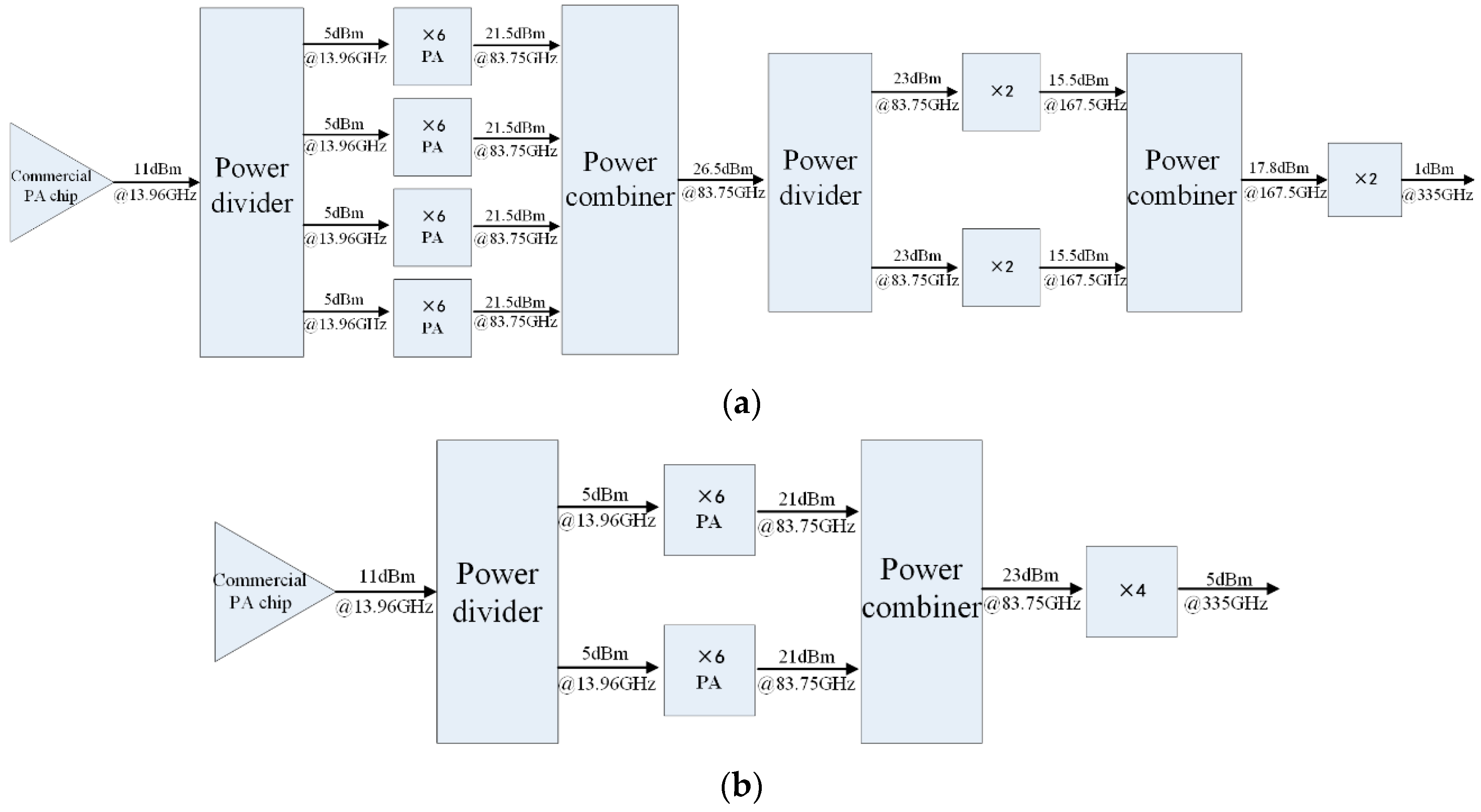
Increasing the efficiency and power capability of the frequency multiplier is the common way to obtain high output power [11,12,13]. For the diodes used in this paper, the safe input power was 24 dBm for a single multiplier. Therefore, power-combined technology was adopted to increase the effective input power. Figure 1 shows the diagram of a 335 GHz solid-state source with different schemes.
A frequency multiplier of order N converts the input sinusoidal signal of frequency F1 and power P1 to an output sinusoidal signal of frequency FN = N × F1 and power PN. Hence, the conversion efficiency of the frequency multiplier is defined as the ratio of PN to P1. For a chain (×N1×N2) of two cascaded multipliers of respective order N1 and N2, the conversion efficiency of the chain is η (N1, N2). A high-order frequency multiplier of order N3 = N1 × N2 usually has a conversion efficiency η (N3) < η (N1, N2) and η (N1, N2) = η (N1) × η (N2). Therefore, in theory, the efficiency of scheme (a) in Figure 1 is higher than that of scheme (b).
Furthermore, the relation of η (N1, N2) = η(N1) × η(N2) is valid only when there is no reflected power by the second multiplier. Besides, the mismatch of the interface between the cascaded multipliers caused by dimension error and assembly error could lead to a loss of power. Consequently, the efficiency of the chain × N1×N2 is not necessarily more than that of the chain × N3 in practical application.
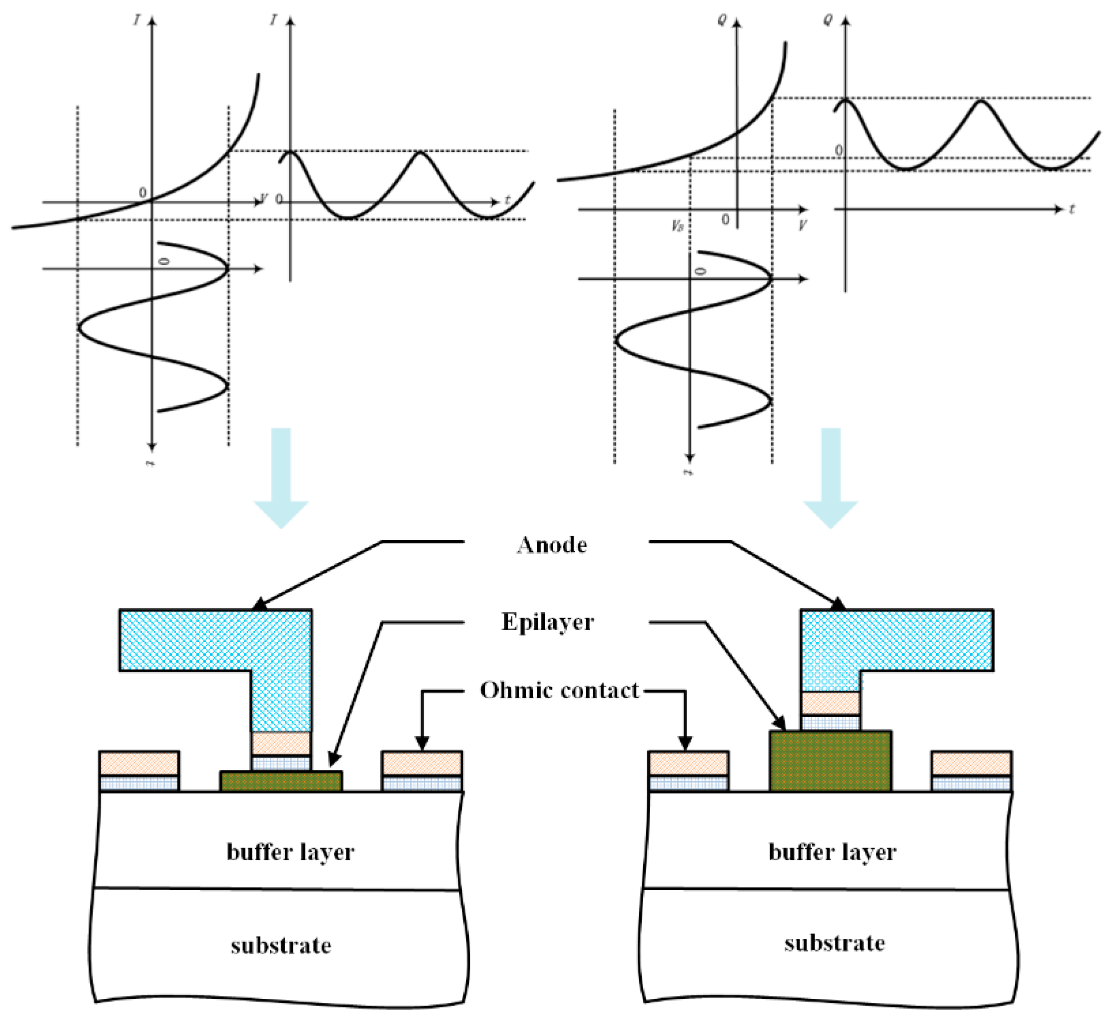
3. Basic Principle of Schottky Diode
The Schottky barrier diode is a two-port device that is important to terahertz frequency multipliers. The diode can be divided into two modes based on operating principle: varistor and varactor. In general, the structure of a Schottky varactor is qualitatively the same as that of a varistor diode. However, the epitaxial layer of the varactor is thicker than that of the varistor, which could increase the breakdown voltage to maximize capacitance variation [14]. Figure 2 shows the cross-sectional view of the Schottky diode. The varistor makes use of a nonlinear resistance characteristic for the mixer, and the varactor is used for frequency multipliers by using a nonlinear capacitance characteristic. The upper part of Figure 2 shows the nonlinear curves of the varistor and varactor.
The diode consists of intrinsic and parasitic parameters. When the frequency increases to the terahertz range, the parasitic parameters of the diode cell caused by its physical structure play an important role in affecting the performance of the frequency multiplier. Hence, the electromagnetic field around the diodes is calculated with full-wave simulation software. As for intrinsic parameters, these primarily include series resistance, zero bias junction capacitance, barrier voltage, and ideal factor. These parameters can be obtained from the IV (Intensity and voltage) or CV (Capacitance and voltage) curve.
4. Design of 335 GHz Source Based on Two-Stage Doubler
The three-dimensional model of a 335 GHz source with cascaded balanced frequency doublers is presented in Figure 3. As shown in the graph, the frequency multiplier is a split-block waveguide design, and a suspended microstrip circuit based on a 50 µm thick quartz substrate is mounted in the channel between the input and output waveguide. The varactor chips are mounted on the suspended microstrip circuit with silver epoxy.
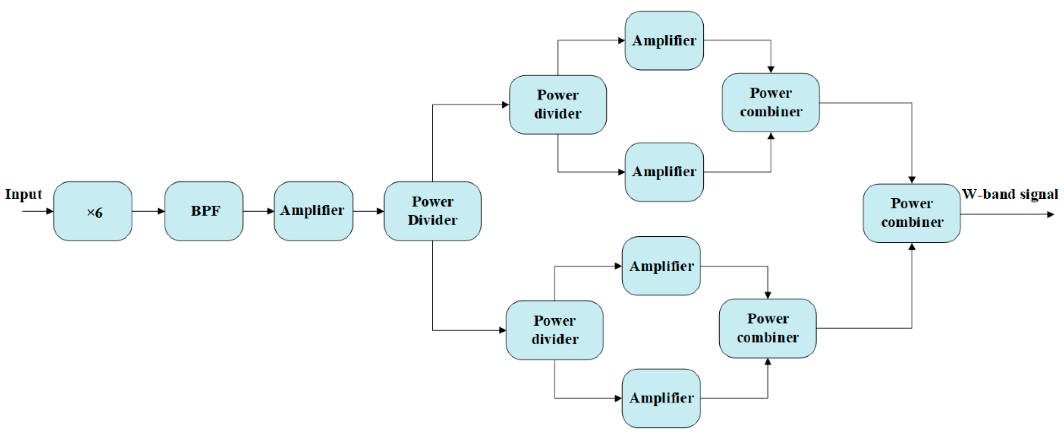
4.1. W-Band High-Power Source
The W-band power source driven by the 167 GHz doubler, which mainly includes a sextupler, a power amplifier, and a four-way power-combining module. The composition block diagram is shown in Figure 4. The sextupler employs a commercially available GaAs MMIC chip HMC1110 fabricated by Analog Devices Company (Norwood, MA, USA), and the power amplifier uses an MMIC chip MAAP-011106 fabricated by M/A-COM Technology Solutions Inc (Lowell, MA, USA). Finally, the measured results indicate that the output power is more than 25 dBm at 81–86 GHz, and that the output power is about 27.5 dBm at 83 GHz when driven by 3 dBm of input power.
4.2. Two-Way Power-Combined 167 GHz Frequency Multiplying Source
Considering the technical requirements and cost, the 167 GHz high-power frequency multiplying source adopts a two-way power-combined scheme. As depicted in Figure 5, the power source includes a power divider/combiner and two identical doublers.
The power divider used in the 167 GHz high-power frequency multiplying source is a Y-type waveguide divider and the phase difference between the two output signals is zero. Furthermore, the second harmonic produced by the doublers has the same phase, and can be combined by using a Y-type waveguide combiner at the output ports. Figure 5 shows the phase relationship of each part in the two branches using the red arrow. Actually, the Y-type power combiner can be regarded as a combination of two-phase shifters and an E–T-type combiner, and the function of the phase shifter is to change the phase of the two-way signal from the same direction to the reverse direction for the T-type combiner.
Generally, the frequency doubler is designed to convert a pump microwave signal to its second harmonic based on the nonlinear voltage-dependence of the diode junction capacitance of the Schottky varactor. To suppress the odd harmonics, the diode array adopted has an anti-series type configuration. The incident signal with the dominant mode of the input rectangular waveguide (TE10) feeds the anti-series diode array. In contrast, the second harmonic would propagate along the suspended microstrip line in an unbalanced mode (TEM). In the 167 GHz doubler design, a 5VA40-13 diode chip provided by Advanced Compound Semiconductor Technologies (Hanau, Germany) was selected, which comprises a linear array of three Schottky junctions. The dimension of the chip is 240 × 60 μm (length and width, respectively) and the semi-insulating GaAs substrate is 35 µm thick.
The equivalent circuit of the balanced doubler is described at the top right of Figure 5. Based on the IV characteristic of the Schottky diode, the output current i can be expressed as [15]:
where is represents the reverse saturation current and Vin represents the junction voltage across the Schottky contact. By using Fourier expansion, Formula (1) is decomposed as follows:
where In (αVin) is the Bessel function of the first kind. Similar to the computational method of the output current, the current in the loop can be expressed as:
From the calculated results, it can be seen that the odd harmonics are suppressed in the output circuit, and thus the second harmonic can be obtained at the output waveguide by using the matching circuit.
4.3. 335 GHz Doubler Based on Discrete Schottky Varactor
Considering the rise of working frequency, the varactor used in the 335 GHz doubler requires a smaller zero bias junction capacitance, and therefore obtains higher cut-off frequency. At the same time, the dimension of the diode chip must be reduced to match the width of the waveguide channel. Finally, the diode chip 137C from Virginia Diodes Inc (Charlottesville, VA, USA). with four anodes in anti-series configuration was applied in the design. To improve the performance of RF ground, the flip-chip mounted method was adopted. The diode chip was glued on the ground points, which are two gold belts on either side of the quartz substrate.
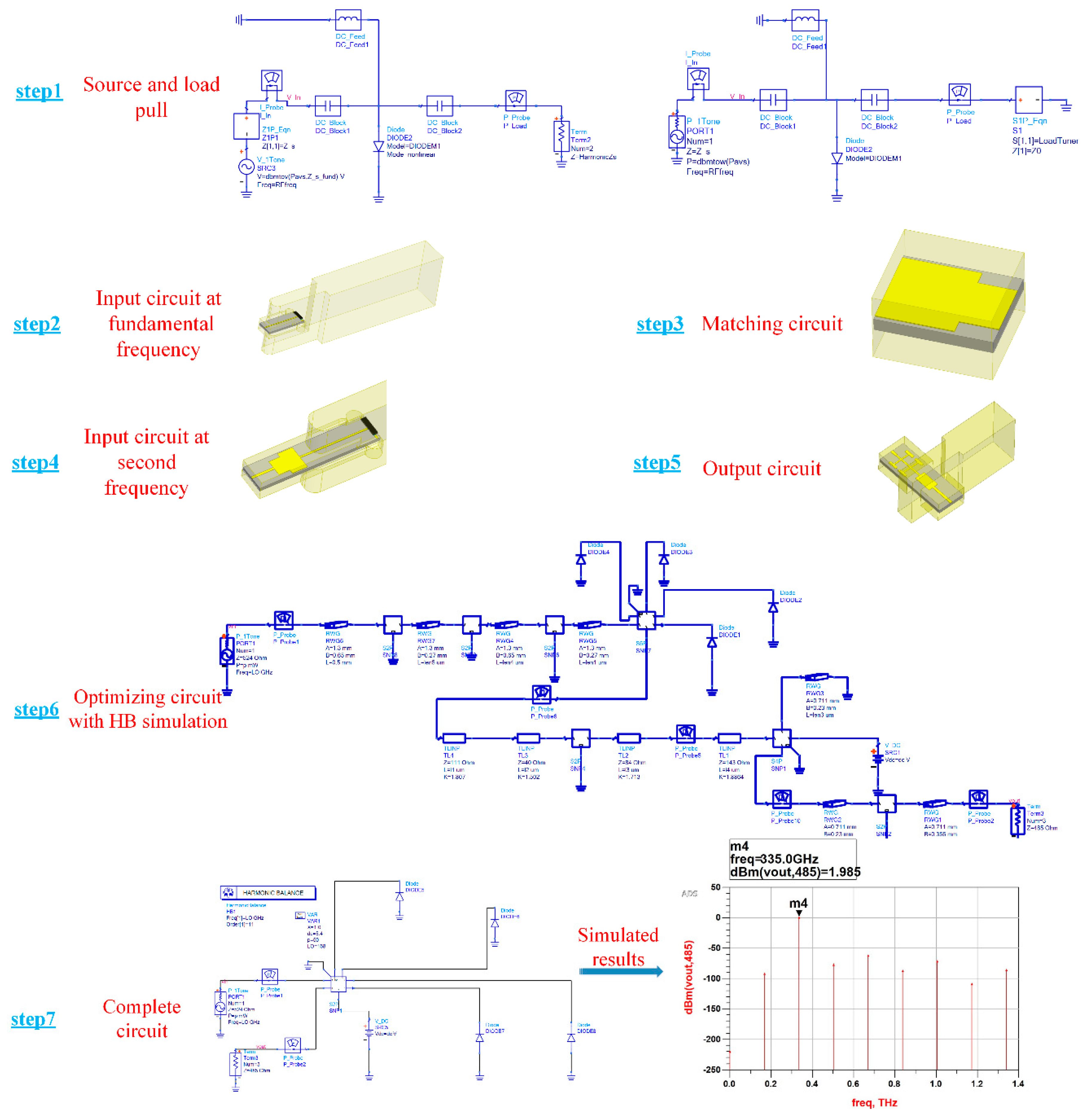
The design process of the 335 GHz balanced doubler is shown in Figure 6. First of all, the impedances of the diode at fundamental and second harmonic are optimized by using source and load-pull under ideal conditions. The diode optimum impedance was found to be Zsource = 33 − j37 Ω and Zload = 16 − j23 Ω. To improve the accuracy of simulation, the field-circuit method is applied in the design process [16,17]. Hence, the doubler is divided into two parts: a linear network, which is analyzed using the finite element method in consideration of the parasitic effects, and the nonlinear behavior of the varactor solved by the harmonic balance method. To reduce the complexity of the problem, the linear part is broken up into three sections: input transition at fundamental and second frequency, output transition, and matching circuit. The signal is coupled through a waveguide-microstrip structure, and the locations of Schottky diodes junction are inserted based on the port impedances (at fundamental frequency) acquired from step 1. Generally, the length of the reduced-height waveguide and location of the input back-short are optimized to achieve a small return loss in the input port. The second harmonic passes through the region between the diodes and input back-short and then is coupled into the output line by matching circuit. Another probe located in the output circuit couples the second harmonic to the standard output waveguide. The abovementioned design process refers to steps 2–5. In the next step, the generated SNP files are imported to the Advanced Design System (ADS) circuit and the characteristic of the diode is added in the nonlinear circuit. Furthermore, the optimization procedure is achieved based on harmonic balance analysis. Finally, the three-dimensional model of the doubler is built according to the optimized results and the calculated S parameter of the complete circuit is exported to the ADS. Now, the doubler model is regarded as a 7-port network. The simulated result of a doubler working at 335 GHz is described at the right side of Figure 6. It clear that the odd harmonics are suppressed in simulation, and that the results coincide with those obtained by Equations (1)–(3).
5. Design of 335 GHz Source Based on Single-Stage Quadrupler
If varactor currents are allowed only at the input and output frequencies, a Schottky diode with ideal CV characteristics cannot generate harmonics higher than the second harmonic. To generate higher harmonics, it is necessary to allow idler currents to flow in the varactor, which could be produced by frequency doubling or frequency mixing.
For a quadrupler, one way to obtain higher harmonics is by doubling and then producing a fourth harmonic by doubling again. Another way is by mixing the second harmonic idler with the fundamental to produce the third harmonic idler first, and by continuing to mix to produce the fourth harmonic output. Actually, the high-order multipliers are most efficient when idler circuits are provided at all idler frequencies. Therefore, the use of idlers could increase the output power and efficiency of reactive frequency multipliers.
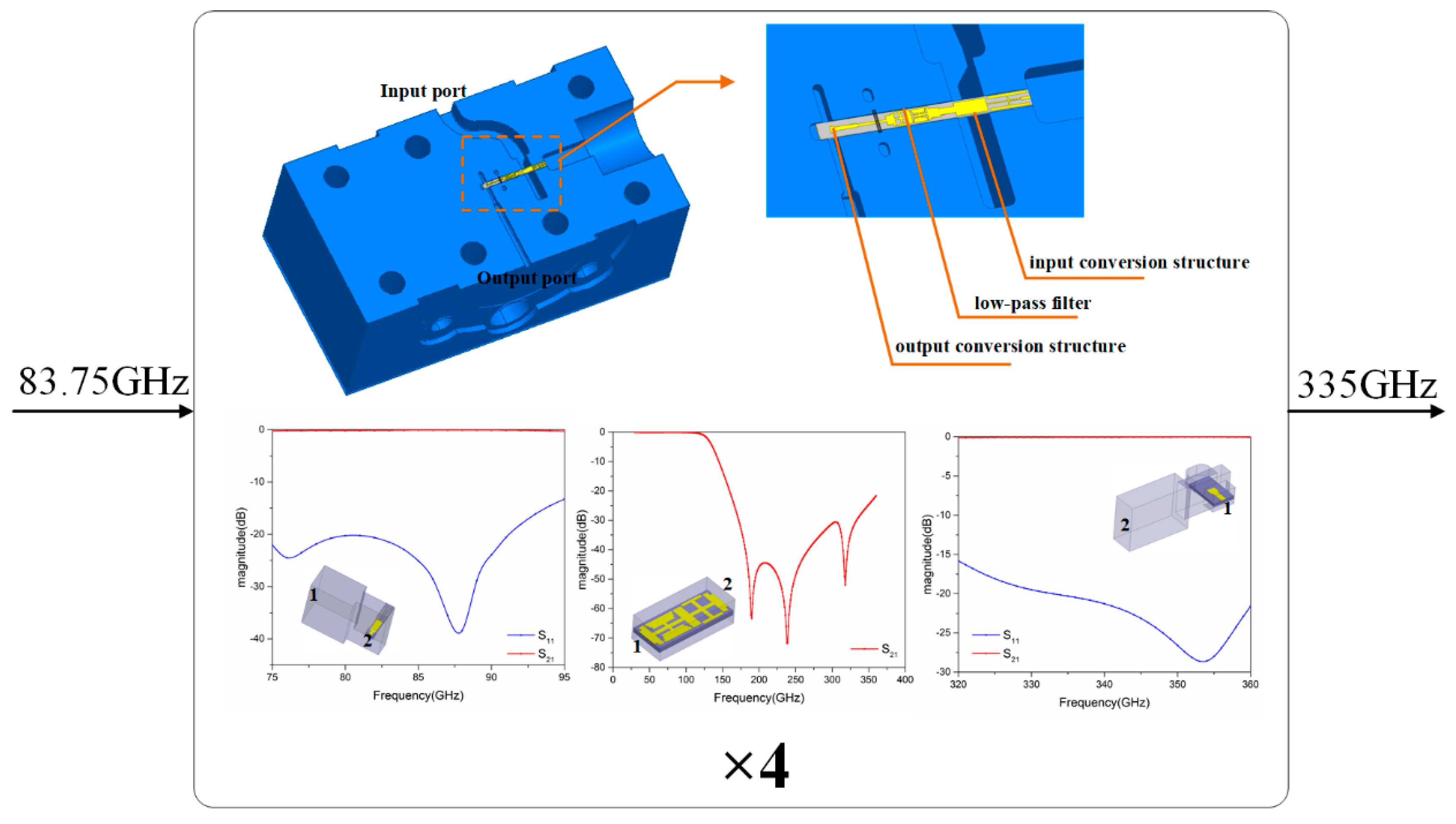
The quadrupler has a suspended microstrip circuit based on a 50 µm thick quartz substrate mounted in the channel with silver epoxy. The input and output ports of the quadrupler are standard full-height WR-12 and WR-2.8 waveguides with waveguide dimensions of 3.1 × 1.65 mm2 and 0.71 × 0.355 mm2, respectively. As described in Figure 7, a compact suspended microstrip resonator (CSMR) low-pass filter follows an input conversion structure (the simulated return loss is below −20 dB from 75 to 90 GHz), and hence the fourth harmonic produced by varactors could prevent leaking from the input port. Compared with the step impedance filter, the CSMR filter has a compacted structure and wide stop band [18]. The simulated result of the CSMR filter in the band of 30–350 GHz are shown in Figure 7. It can be seen from the graph that the insert loss is lower than 0.3 dB in the pass band, while the side rejection is better than 20 dB from 160 to 350 GHz. Finally, another probe located in the output circuit couples the fourth harmonic to the standard output waveguide, and the simulated return loss is better than 15 dB in the frequency range of 320–360 GHz. All passive networks, such as the low-pass filter, input and output waveguide-to-microstrip transition, and diode passive part, are analyzed by EM simulators. When the sub-circuits are optimized, the complete quadrupler circuit is simulated. The nine port S-parameters of this simulation are extracted and then combined with a nonlinear diode to model the multiply efficiency in the circuit simulator. This process is usually repeated for the further optimization of the quadrupler multiply efficiency.
6. Measurements and Discussion
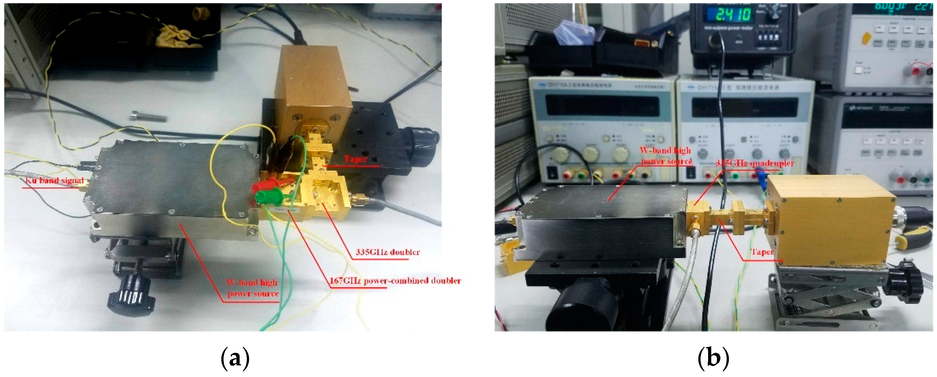
The block diagram of the measurement setup is illustrated in Figure 8. An Agilent analog signal generator E8257D (Santa Clara, CA, USA) is followed by the W-band power source to generate the signal in the 81–86 GHz band. The output power of the frequency multipliers is measured by a PM4 power meter (Charlottesville, VA, USA). Moreover, a Sub-Miniature-A (SMA) (type KFD55(Xi’an, China)) is connected to the main transmission circuit using gold wire bonding and an external sliding rheostat connected to the SMA port so as to bias the varactor.
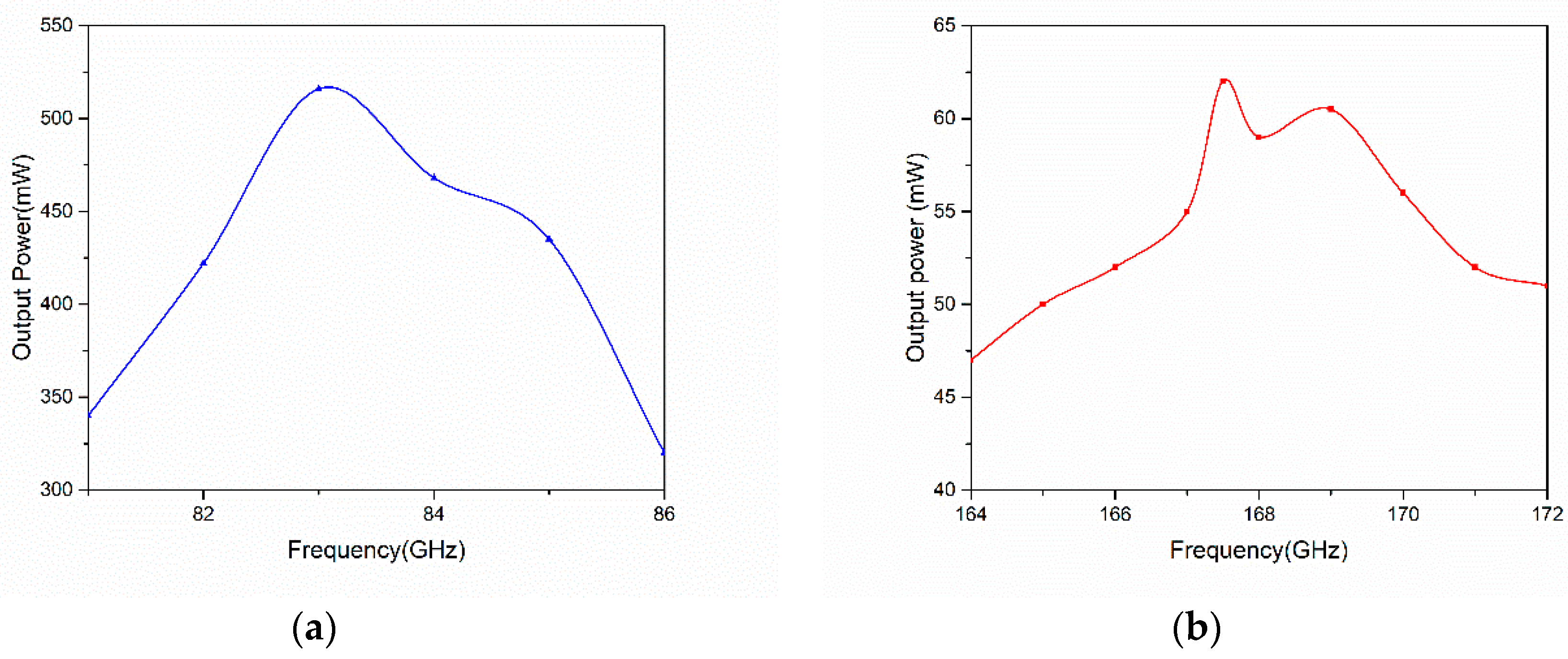
Figure 9a shows the measured results of the W-band source. The measured output power is more than 310 mW from 81 GHz to 86 GHz, and the maximum power is about 560 mW at 83 GHz. In the measurement of the quadrupler, the input power is about 200 mW to make sure the diodes work safely, and hence an attenuator is added. The measured output power of the 167 GHz power-combined doubler is shown in Figure 9b. It was found that the power is more than 45 mW at 164–172 GHz, and the highest output power is 62 mW at 167.5 GHz.
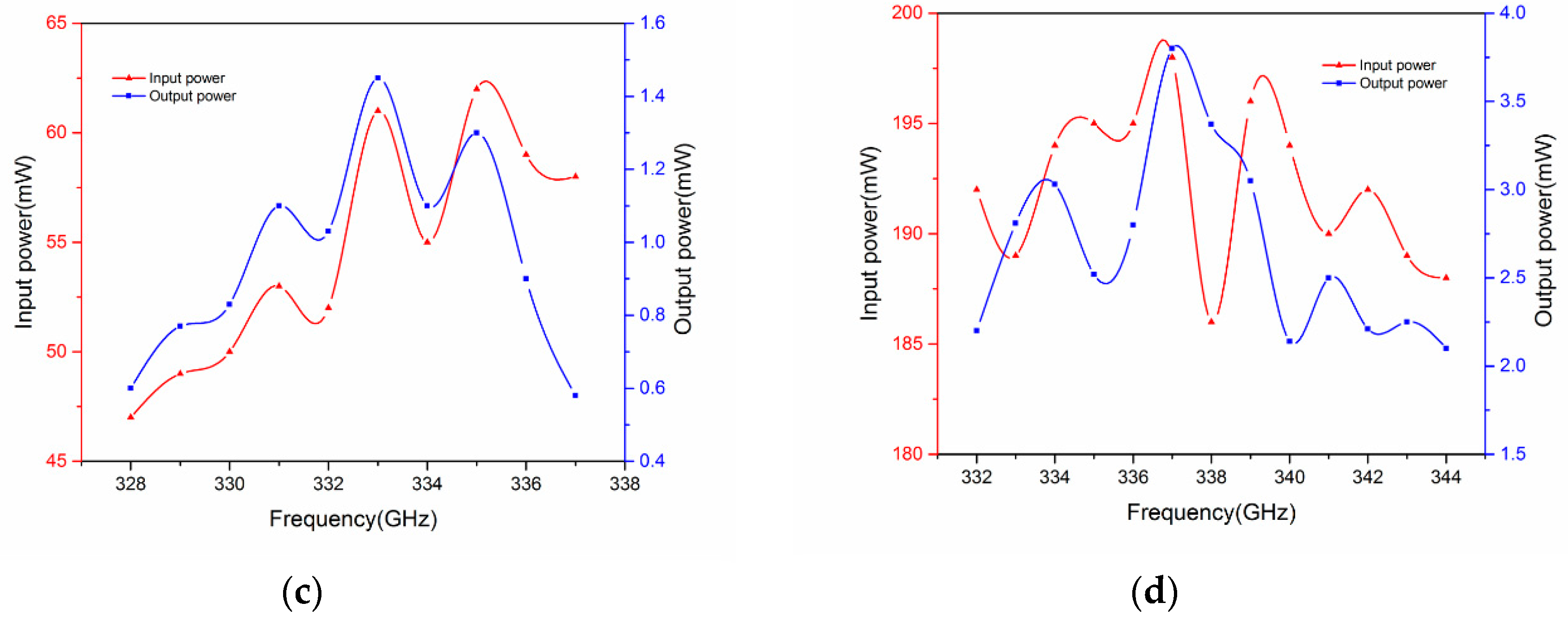
The measured results of the 335 GHz source based on two cascaded doublers are shown in Figure 9c. The measured output power of the 335 GHz doubler is more than 0.5 mW at 328–337 GHz and the maximum output power is about 1.4 mW at 333 GHz. The relation of the single-stage quadrupler 335 GHz source output versus pumping power is described in Figure 9d. The measured typical output power is 2.5 mW at 332–344 GHz, and the highest measured output power of 3.8 mW is measured at 337 GHz with an input power of 198 mW.
Table 1 and Table 2 illustrate a comparison of some reported multipliers. A recent development of terahertz solid circuits in China caused a regression in advanced semiconductor technology such as Schottky diode technology, membrane technology, transferred substrate technology, and so on. The result is that an integrated circuit is difficult to realize and the design of the frequency multiplier needs to use a discrete circuit with a higher loss transmission line. The performance of the frequency multipliers presented in this paper reached the same level as that achieved by research institutions abroad, and has a leading position at home. Furthermore, the design using discrete diodes is easy to realize and the cost is relatively low.
To ensure that the 167 GHz doubler is working safely, the input power produced by the W-band source is controlled below 280 mW and the typical output power of the doubler is, accordingly, 55 mW. Hence the typical efficiency of the 167 GHz doubler is about 20%. The typical efficiency of the 335 GHz doubler is 2% with typical input and output power values of 55 and 1.1 mW, respectively. To summarize, the efficiency of the frequency multiplier chain is about 0.4%. In contrast, the typical input and output power values of a single-stage quadrupler are 190 mW and 2.8 mW, and said quadrupler has a higher efficiency of about 1.5%. However, it is difficult to say whether it is better to realize a high-order multiplier via a single-stage process or by a cascade of two or more low-order multipliers. The decision could be made in accordance with specific conditions.
7. Conclusions
A solid-state frequency multiplier chain based on two schemes has been designed and tested in this paper. For the first option, the measured highest output power was about 1.4 mW at 333 GHz and more than 0.5 mW at 328–337 GHz. For the second option, the measured typical output power was 2.5 mW at 332–344 GHz, and the highest measured output power was 3.8 mW at 337 GHz. The research content provides the means to generate a terahertz signal above 300 GHz. Our future work will aim at the design of a G-band, higher output power source, and at the increased efficiency of the frequency multiplier working in the sub-millimeter region.
Author Contributions
Conceptualization, methodology, software, and writing, J.M., D.Z., and G.J.; formal analysis, C.Y. and C.J.; visualization, J.M. and S.L.
Funding
This research received no external funding.
Conflicts of Interest
The authors declare no conflict of interest.
References
- Chattopadhyay, G. Terahertz antennas and systems for space borne platforms. In Proceedings of the Fourth European Conference on Antennas and Propagation (IEEE), Barcelona, Spain, 12–16 April 2010. [Google Scholar]
- Arora, A.; Luong, T.Q.; Krüger, M.; Kim, Y.J.; Nam, C.H.; Manz, A.; Havenith, M. Terahertz-time domain spectroscopy for the detection of PCR amplified DNA in aqueous solution. Analyst 2012, 137, 575–579. [Google Scholar] [CrossRef] [PubMed]
- Waters, J.W.; Froidevaux, L.; Harwood, R.S.; Jarnot, R.F.; Pickett, H.M.; Read, W.G.; Siegel, P.H.; Cofield, R.E.; Filipiak, M.J.; Holden, J.R.; et al. The earth observing system microwave limb sounder (EOS MLS) on the aura satellite. IEEE Trans. Geosci. Remote Sens. 2006, 44, 1075–1092. [Google Scholar] [CrossRef]
- Maestrini, A.; Ward, J.; Chattopadhyay, G.; Schlecht, E.; Mehdi, I. Terahertz Sources Based on Frequency Multiplication and Their Applications. Frequenz 2008, 62, 118–122. [Google Scholar] [CrossRef]
- Moyna, B.P.; Charlton, J.E.; Lee, C.; Parker, R.J.; Oldfield, M.M.; Matheson, D.N.; Peter, M.; Kangas, V. Design of a sub-millimetre wave airborne demonstrator for observations of precipitation and ice clouds. In Proceedings of the Antennas and Propagation Society International Symposium, Charleston, SC, USA, 1–5 June 2009. [Google Scholar]
- Imran, M.; Bertrand, T.; Robert, L.; Alain, M.; John, W.; Erich, S.; John, G.; Choonsup, L.; Goutam, C.; Frank, M. High-power local oscillator sources for 1–2 THz. Int. Soc. Opt. Eng. 2010, 7741. [Google Scholar] [CrossRef]
- Chattopadhyay, G.; Schlecht, E.; Ward, J.S.; Gill, J.J.; Javadi, H.H.; Maiwald, F.; Mehdi, I. An All-Solid-State Broad-Band Frequency Multiplier Chain at 1500 GHz. IEEE Trans. Microw. Theory Tech. 2004, 52, 1538–1547. [Google Scholar] [CrossRef]
- Yao, C.; Wei, X.; Luo, Y.; Zhou, M. A 210 GHz power-combined frequency multiplying source with output power of 23.8 mW. Frequenz 2017, 71, 523–530. [Google Scholar] [CrossRef]
- Zhang, Y.; Lu, Q.-Q.; Liu, W.; Li, L.; Xu, R.-M. Design of a 220 GHz frequency tripler based on EM model of Schottky diodes. J. Infrared Millim. Waves 2014, 33, 405–411. [Google Scholar]
- Yao, C.F.; Zhou, M.; Luo, Y.S.; Wang, Y.G.; Xu, C.H. 150 GHz and 180 GHz fixed-tuned frequency multiplying sources with planar Schottky diodes. J. Infrared Millim.Waves 2013, 32, 102–107. [Google Scholar] [CrossRef]
- Maestrini, A.; Ward, J.S.; Tripon-Canseliet, C.; Gill, J.J.; Lee, C.; Javadi, H.; Chattopadhyay, G.; Mehdi, I. In-phase power-combined frequency triplers at 300 GHz. IEEE Microw. Wirel. Compon. Lett. 2008, 18, 218–220. [Google Scholar] [CrossRef]
- Siles, J.V.; Maestrini, A.; Alderman, B.; Davies, S.; Wang, H.; Treuttel, J.; Leclerc, E.; Narhi, T.; Goldstein, C. A Single-Waveguide in-Phase Power-Combined Frequency Doubler at 190 GHz. IEEE Microw. Wirel. Compon. Lett. 2011, 21, 332–334. [Google Scholar] [CrossRef]
- Gupta, M.S. Degradation of power combining efficiency due to variability among signal sources. IEEE Trans. Microw. Theory Tech. 1992, 40, 1031–1034. [Google Scholar] [CrossRef]
- Faber, M.T.; Chramiec, J.; Adamski, M.E. Microwave and Millimeter-Wave Diode Frequency Multipliers; Artech House: Boston, MA, USA; London, UK, 1995. [Google Scholar]
- Penfield, P.; Rafuse, R.P. Varactor Applications; MIT Press: London, UK, 1962. [Google Scholar]
- Thomas, B.; Treuttel, J.; Alderman, B.; Matheson, D.; Narhi, T. Application of substrate transfer to a 190 GHz frequency doubler and 380 GHz sub-harmonic mixer using MMIC foundry Schottky diodes. In Proceedings of the Millimeter and Submillimeter Detectors and Instrumentation for Astronomy IV, Marseille, France, 23–28 June 2008. [Google Scholar]
- Meng, J.; Zhang, D.; Jiang, C. Research on the practical design method of 225 GHz tripler. J. Infrated Millim. Waves 2015, 34, 190–195. [Google Scholar]
- Yang, X.; Zhang, B.; Fan, Y.; Zhong, F.Q.; Chen, Z. Design of improved CMRC structure used in terahertz subharmonic pumped mixer. In Proceedings of the 12th IEEE International Conference on Communication Technology, Nanjing, China, 11–14 November 2010. [Google Scholar]
- Vadiodes. Available online: http://www.vadiodes.com (accessed on 21 August 2019).
- Chen, Z.; Chen, X.; Cui, W.; Li, X.; Ge, J. A High-Power G-band Schottky local oscillator chain for submillimeter wave heterodyne detection. J. Infrared Milli. Terahertz Waves 2015, 36, 430–444. [Google Scholar] [CrossRef]
- Liu, H.; Powell, J.; Viegas, C.; Cairns, A.A.; Alderman, B. A 332 GHz frequency doubler using flip-chip mounted planar Schottky diodes. In Proceedings of the Asia-Pacific Microwave Conference, Nanjing, China, 6–9 December 2015. [Google Scholar]
- Xiao, Z. Research on 330 GHz Multiplier Based on Planar Schottky Diode; University of Electronic Science and Technology of China: Chengdu, China, 2017. [Google Scholar]
Figure 1.
(a) Block diagram of the 335 GHz frequency multiplier based on a two-stage doubler. (b) Block diagram of the 335 GHz frequency multiplier based on a single-stage quadrupler.
Figure 1.
(a) Block diagram of the 335 GHz frequency multiplier based on a two-stage doubler. (b) Block diagram of the 335 GHz frequency multiplier based on a single-stage quadrupler.

Figure 2.
Structures and operating principles of the Schottky varistor and varactor.

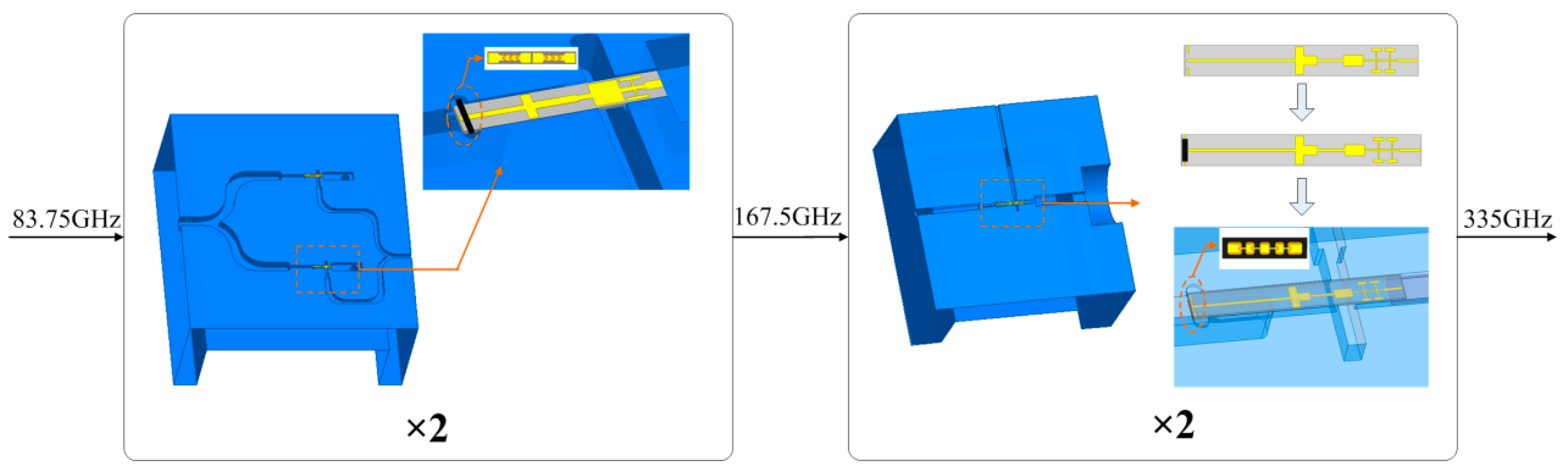
Figure 3.
The three-dimensional model of the 335 GHz source based on a two-stage doubler.

Figure 4.
The block diagram of the W-band source.

Figure 5.
The structure of the 167 GHz doubler based on the two-way power-combined technology.

Figure 6.
Design process of a 335 GHz balanced doubler with the field-circuit method.

Figure 7.
Three-dimensional model of the 335 GHz source based on a single-stage quadrupler.

Figure 8.
(a) Photo of the assembled 335 GHz source with two cascaded doublers. (b) Photo of the assembled 335 GHz source with a single-stage quadrupler.
Figure 8.
(a) Photo of the assembled 335 GHz source with two cascaded doublers. (b) Photo of the assembled 335 GHz source with a single-stage quadrupler.

Figure 9.
(a) Measured output power of the W-band source. (b) Measured output power of the 167 GHz high-power source. (c) Measured input and output power of the 335 GHz source based on a two-stage doubler. (d) Measured input and output power of the 335 GHz source based on a single-stage quadrupler.
Figure 9.
(a) Measured output power of the W-band source. (b) Measured output power of the 167 GHz high-power source. (c) Measured input and output power of the 335 GHz source based on a two-stage doubler. (d) Measured input and output power of the 335 GHz source based on a single-stage quadrupler.


Table 1.
Performance comparison of the doubler around 170 GHz.
| References | Technology | Frequency (GHz) | Max Output Power (mW) | Typical Efficiency |
|---|---|---|---|---|
| [19] from VDI (Virginia Diodes, Inc.) | ×2 integrated | 110–170 | 24 | 8% |
| [20] from NUIST (Nanjing University of Information Science and Technology) | ×2 discrete | 176–196 | 40 | 12% |
| This paper | ×2 discrete | 164–172 | 62 | 20% |
Table 2.
Performance comparison of the frequency multipliers above 300 GHz.
| References | Technology | Frequency (GHz) | Max Output Power (mW) | Typical Efficiency |
|---|---|---|---|---|
| [19] from VDI | ×2 integrated | 220–330 | 3 | 6% |
| [21] from RAL (Rutherford Appleton Laboratory) | ×2 discrete | 330–336 | 1.2 | 2% |
| [22] from UESTC (University of Electronic Science and Technology of China) | ×3 discrete | 320–342 | 0.149 | 0.3% |
| This paper | ×2 discrete | 328–337 | 1.4 | 2% |
| ×4 discrete | 332–344 | 3.8 | 1.5% |
© 2019 by the authors. Licensee MDPI, Basel, Switzerland. This article is an open access article distributed under the terms and conditions of the Creative Commons Attribution (CC BY) license (http://creativecommons.org/licenses/by/4.0/).
Share and Cite
MDPI and ACS Style
Meng, J.; Zhang, D.; Ji, G.; Yao, C.; Jiang, C.; Liu, S. Design of a 335 GHz Frequency Multiplier Source Based on Two Schemes. Electronics 2019, 8, 948. https://doi.org/10.3390/electronics8090948
AMA Style
Meng J, Zhang D, Ji G, Yao C, Jiang C, Liu S. Design of a 335 GHz Frequency Multiplier Source Based on Two Schemes. Electronics. 2019; 8(9):948. https://doi.org/10.3390/electronics8090948
Chicago/Turabian StyleMeng, Jin, Dehai Zhang, Guangyu Ji, Changfei Yao, Changhong Jiang, and Siyu Liu. 2019. "Design of a 335 GHz Frequency Multiplier Source Based on Two Schemes" Electronics 8, no. 9: 948. https://doi.org/10.3390/electronics8090948
Note that from the first issue of 2016, this journal uses article numbers instead of page numbers. See further details here.