1. Introduction
Conventional metal oxide semiconductor field-effect transistors (MOSFETs) with carrier diffusion drift are susceptible to the short-channel effect when device sizes decrease, which can increase the power consumption and off-state leakage current [
1,
2,
3]. In addition, the subthreshold swing (SS) value of MOSFETs has a minimum limit of 60 mV/Dec at room temperature due to the statistical distribution of thermodynamics, so the switching ratio decreases [
4,
5]. In order to improve the performance of smaller devices, researchers have studied many new materials and new device structures. Two-dimensional materials have excellent physical, chemical, and optical properties. Meanwhile, materials such as graphene [
6], MoS
2 [
7], and PdSe
2 [
8] have adjustable electronic properties and bandgap width. It is these excellent characteristics that give two-dimensional materials great application potential for use in electronic devices. The new device structures that have been researched include multi-gate devices that improve electrostatic characteristics [
9], ultrathin silicon-on-insulator (UTSOI) MOSFETs [
10], gate-all-around (GAA) MOSFETs [
11], and Fin field-effect transistors (Fin-FETs) [
12]. Device performance can also be improved by using narrow bandgap semiconductor materials, high-k gate dielectric materials such as III–V-based and Si
1-xGe
x-based devices [
13,
14], and tunneling field-effect transistors (TFETs) [
15,
16]. TFETs have a lower SS value and off-state current, so they can obtain a larger voltage gain and noise margin in inverter circuit applications [
17]. However, the switching ratio and frequency characteristics are far from ideal in TFETs, and the fabrication processes are complicated, which can limit their application in digital circuits.
To improve the analog/radio frequency (RF) performance and simplify the fabrication processes of TFETs, a doping-less tunnel field-effect transistor (DLTFET) is proposed [
18,
19]. A DLTFET can form heavily doped source and drain regions using the appropriate metal electrode work functions. Due to the absence of an abrupt junction, the fabrication processes of DLTFETs are simpler, and random doping fluctuations have no effect on device performance [
20,
21,
22]. Therefore, it is possible to produce DLTFET devices more innovatively with the development of fabrication processes, such as the etching process, epitaxial growth process, and atomic layer deposition (ALD) process. A larger on-state current can also be obtained when device sizes decrease. However, the disadvantages of DLTFETs are their larger off-state current, power consumption, and lower switching ratio, so their use is not competitive [
23].
In this paper, a DLTFET with Si
0.6Ge
0.4 heterojunction (H-DLTFET) is proposed using TCAD simulation in order to improve the on/off current ratio and the analog/RF performance. Compared with conventional DLTFETs, H-DLTFETs differ in that their source regions and channel regions use the narrow bandgap semiconductor material germanium and the high carrier mobility material Si
0.6Ge
0.4. The Ge–Si tunneling junction can decrease the effective tunneling length, thereby increasing the on-state current [
24]. At the same time, it is possible to reduce the leakage current by the valence band energy difference between germanium and silicon, which is caused by the valence band holes in the off-state. The structure of this paper is organized as follows: First, the device structures and simulation methods of a DLTFET and a H-DLTFET are introduced, and then, the input and output characteristics of the DLTFET and H-DLTFET are discussed. Next, the operating mechanism of the H-DLTFET is studied, and the effect of device size on the performance of the H-DLTFET is analyzed. The C-V and frequency characteristics are then researched. Finally, the conclusions of this paper are presented.
2. Device Structure and Simulation Method
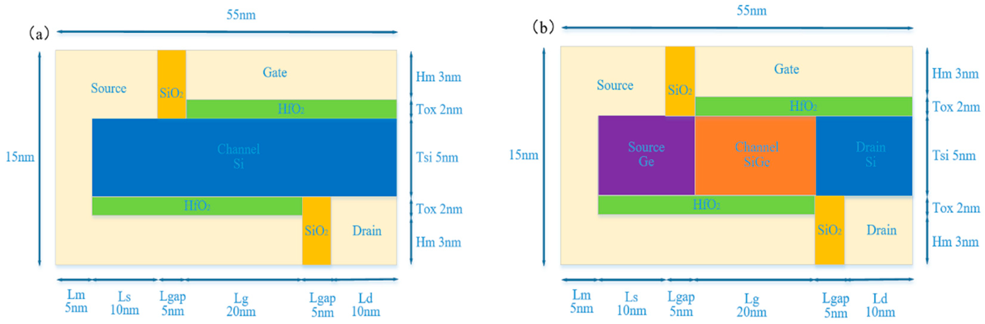
Figure 1a,b shows the structural diagrams of a conventional DLTFET and the proposed H-DLTFET. In
Figure 1, the device sizes are both the same, but the source and channel materials are different. The heavily doped source and drain regions are generated by the charge plasma, and the abrupt PN junction is formed between the source and the channel, both of which are consistent with conventional TFETs [
25]. The gate and the source with different work functions are located on both sides of the channel, the energy band of the overlapping region between the gate and the source is bending, and the line tunneling is formed from the bottom to the top of the channel so that the electron tunnel efficiency can be improved.
Unlike the conventional DLTFET, the semiconductor materials Ge and Si0.6Ge0.4 in H-DLTFETs were used as the source and channel materials in order to provide higher carrier mobility. The energy band of the tunneling junction became steeper, and the tunneling efficiency became higher because of the Si0.6Ge0.4 heterojunction between the source and the channel, which greatly improved the on/off current ratio and frequency characteristics. The specific simulation parameters of the DLTFET and H-DLTFET were as follows: the length of the source region Ls, channel Lg, and drain region Ld were 15 nm, 20 nm, and 15 nm, respectively; the doping concentration Nc = 5 × 1018 cm−3; the gate dielectric layer thickness of HfO2 Tox1 = 2 nm; the gap-layer thickness of SiO2 Tox2 = 5 nm; the channel layer thickness Hc = 5 nm; the source work function φSource = 5 eV; the gate work function φGate = 3.8 eV; and the drain work function φDrain = 4.2 eV.
In this paper, the simulation was based on SILVACO ATLAS. The non-local band-to-band tunneling (BTBT) model was used to analyze the non-local generation of electrons and holes and was used to accurately simulate the electronic tunneling process. Considering the effect of the channel doping region, the bandgap narrowing model was included. The H-DLTFET simulation models also included the Schokely–Read–Hall recombination, Fermi statistics, and the electric field model [
26]. The C-V and frequency characteristics were obtained using an operating frequency of 1 MHz.
3. Results and Discussion
The H-DLTFET had the same device structure, size parameters, and physical models as the conventional DLTFET, except that the source region used the narrow bandgap semiconductor material germanium with larger channel carrier mobility and a smaller bandgap. It also had good compatibility with the silicon process, which decreased the leakage current. The channel region used the high carrier mobility material Si0.6Ge0.4, and the forbidden bandwidth and band structure changed with the changes in the germanium content, which resulted in higher carrier mobility and smaller tunneling barrier width. The energy band and effective tunneling length of the tunneling junction both became steeper and shorter because of the Ge–Si heterojunction, which improved the carrier tunneling efficiency, switching speed, and on-state current.
This section consists of two parts. In the first part, the input/output characteristics of the DLTFET and H-DLTFET are compared, and then, the operating mechanism of the H-DLTFET is analyzed. The effects of the source work function, gate oxide dielectric thickness, and Ge content on the performance of the H-DLTFET are then discussed. Finally, the second part compares the C-V characteristics and the analog/RF performance and then analyzes the cutoff frequency and gain bandwidth (GBW) product of the DLTFET and H-DLTFET.
3.1. Input and Output Characteristics
Figure 2a shows the transfer characteristics of the DLTFET and H-DLTFET when the drain voltage was 1 V. The maximum on-state current of the DLTFET was 83 μA/μm, whereas the maximum on-state current of the H-DLTFET could reach 169 μA/μm. Meanwhile, compared with the conventional DLTFET, the on/off current ratio of the H-DLTFETs increased by three orders of magnitude due to the lower off-state current. The average SS value could be extracted when the drain current rose from 10
−6 to 1 μA/μm. The average SS values of the DLTFET and H-DLTFET were 26.7 mV/Dec and 15.2 mV/Dec, respectively. At the same time, the minimum SS values of the DLTFET and H-DLTFET were 6.7 mV/Dec and 3.9 mV/Dec, respectively. The H-DLTFET had a larger line tunneling current due to the Si
0.6Ge
0.4 heterojunction, which could improve the on-state current and SS value. Therefore, the H-DLTFET has great potential in the emerging market of ultra-low bio-equipment.
As an important parameter, the transconductance (
gm) was used to evaluate the simulation performance of the device, which was defined as the first derivative of the transfer characteristic [
27], and the value of
gm is provided by Equation (1):
As shown in
Figure 2b, the maximum
gm value of the DLTFET was 81.5 μS/μm and the maximum
gm value of the H-DLTFET was 198.8 μS/μm, so the
gm value of the H-DLTFET was almost doubled in comparison with the conventional DLTFET.
Figure 3a,b shows the output characteristics of the DLTFET and the H-DLTFET according to the different gate voltages. At first, the drain current increased linearly with the drain voltage, and the output saturation drain currents of the DLTFET and the H-DLTFET were 83.5 μA/μm and 166.9 μA/μm when
Vg = 2 V and
Vd = 1 V, respectively. Therefore, the output current of the H-DLTFET was much higher than that of the DLTFET.
3.2. The Operating Mechanism of H-DLTFETs
The operating mechanism of the H-DLTFET is explained in
Figure 4 and
Figure 5.
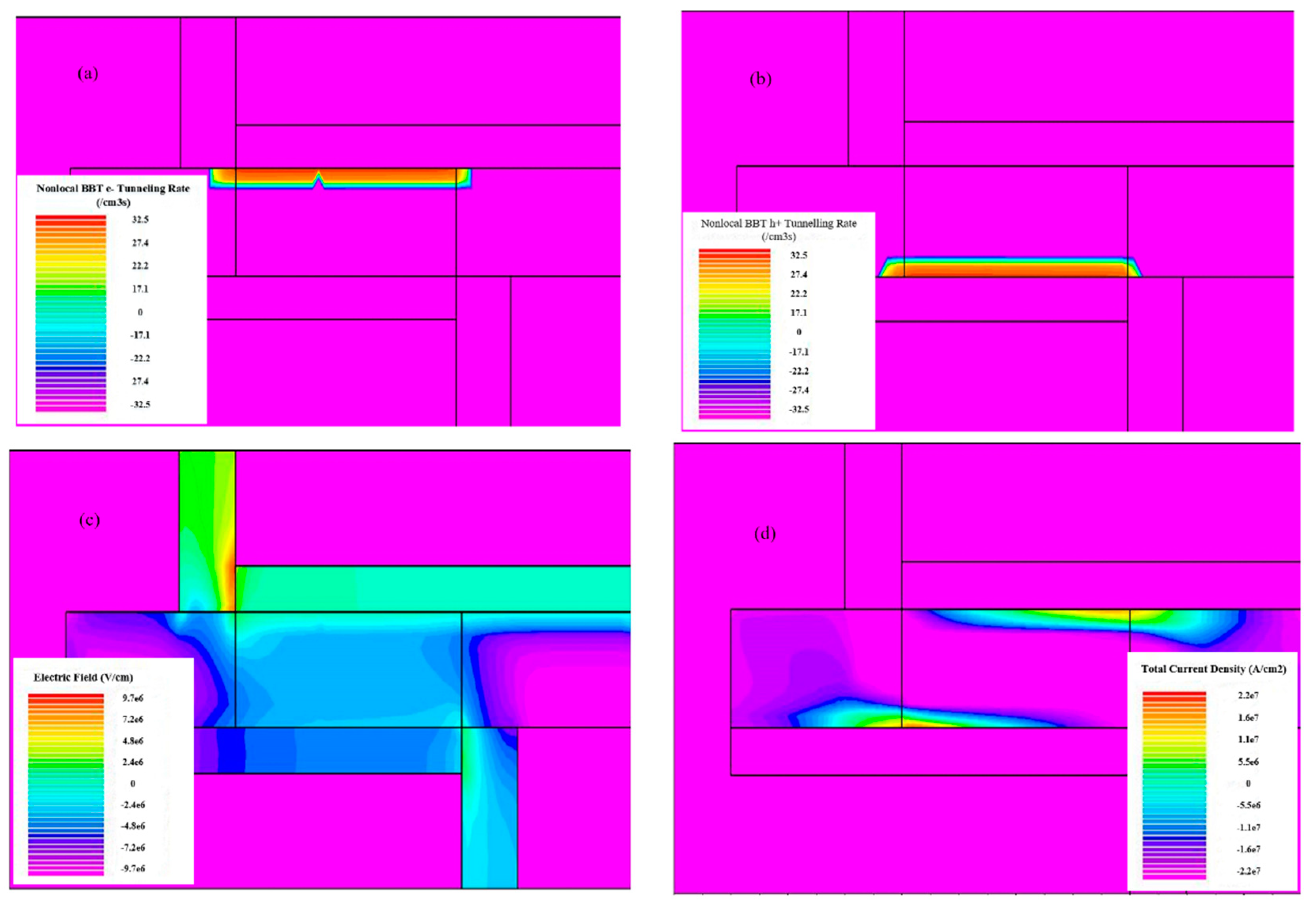
Figure 4a,b shows the electron and hole BTBT generation rates in the on-state. Line tunneling occurred in the alignment region between the gate and the source, and the carrier tunneling rate was evenly distributed along the tunnel junction. In
Figure 4c, the electric field and the BTBT rate of the tunneling junction increased due to the Si
0.6Ge
0.4 heterojunction, so the on-state current increased. In addition, the total current density of the H-DLTFET, according to the on-state, was researched in order to understand the operating mechanism, as shown in
Figure 4d. The electrons from the source region and the channel bottom region could be easily absorbed by the drain region to form the tunneling leakage current [
28,
29].
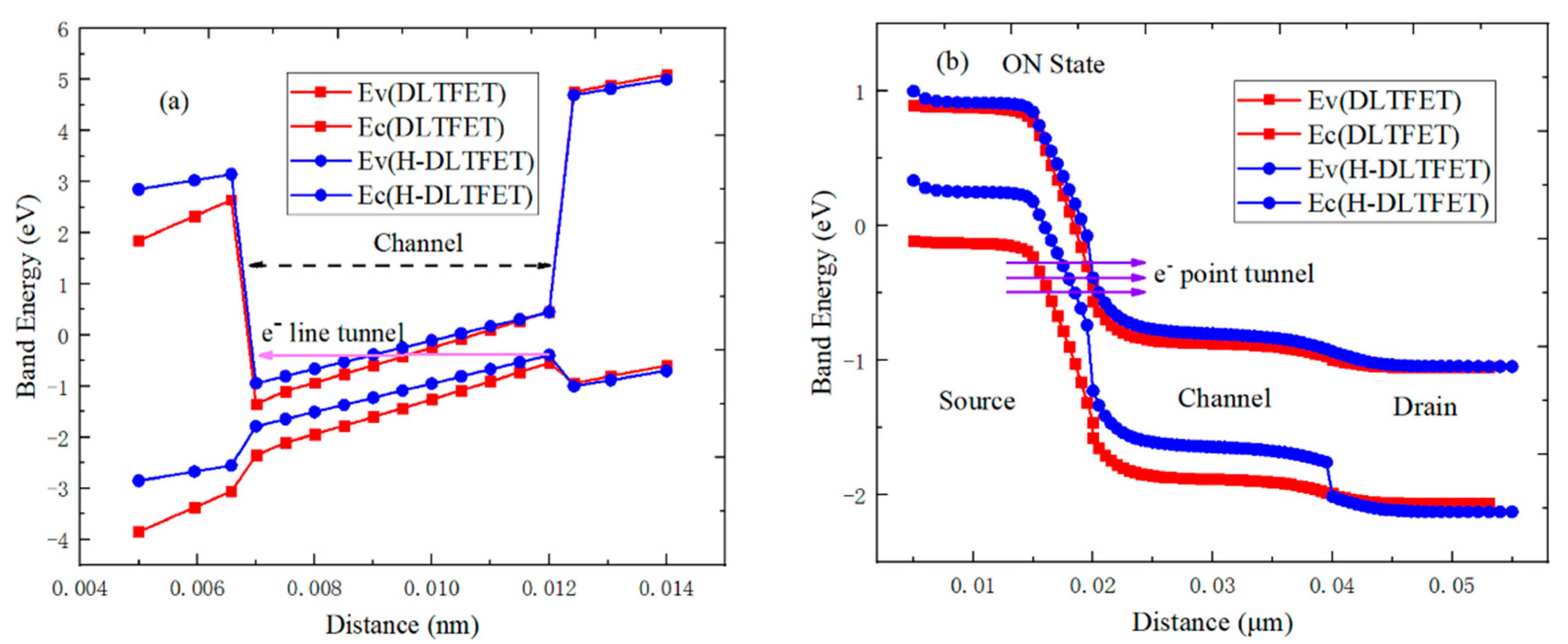
Figure 5 shows the on-state energy band of the DLTFET and the H-DLTFET when they were in different locations. As shown in
Figure 5a, the valence band at the bottom of the channel was aligned with the conduction band at the top of the channel, and many electrons tunneled from the bottom of the channel to the top of the channel to form the line tunneling current. The channel of the H-DLTFET used Si
0.6Ge
0.4 material to provide higher carrier mobility. The source with the higher work function could accumulate many holes at the bottom of the channel, and the electrons could be accumulated by the top channel when a lower work function and a higher voltage were applied to the gate. Therefore, the line tunneling current could be generated in the channel region due to the pseudo-mutation PN junction [
30]. It can be seen in
Figure 5b that the tunneling barrier width of the H-DLTFET between the source and the channel was lower than that of the DLTFET, which could allow more electrons to tunnel from the source to the channel. The narrower the tunneling barrier, the higher the point tunneling current.
3.3. Effect of Device Sizes on the Performance of H-DLTFETs
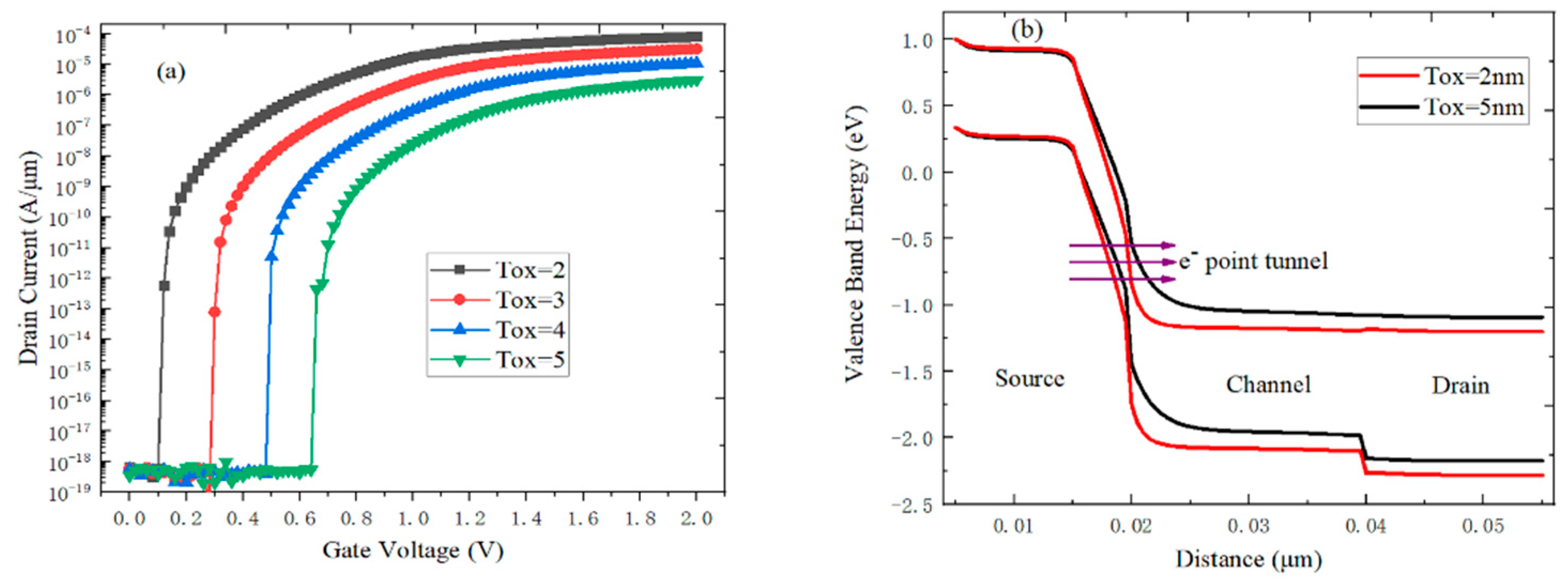
Figure 6 shows the effect of gate oxide dielectric thickness (T
ox) on the transfer characteristics and energy band of the H-DLTFET. As shown in
Figure 6a, the on-state current and switching ratio of the H-DLTFET increased, and the transfer characteristic curve shifted to the left significantly when the T
ox decreased from 5 to 2 nm. The reason for this is that the higher surface potential difference between the gate and the source resulted in a lower tunneling barrier width. The energy band and the electric field of the source/channel tunneling junction then became steeper and higher as the T
ox decreased, and the point tunneling current increased, as shown in
Figure 6b. Therefore, the H-DLTFET with its thinner gate dielectric was easier to turn on, and the transfer characteristic curve shift to the left was greater.
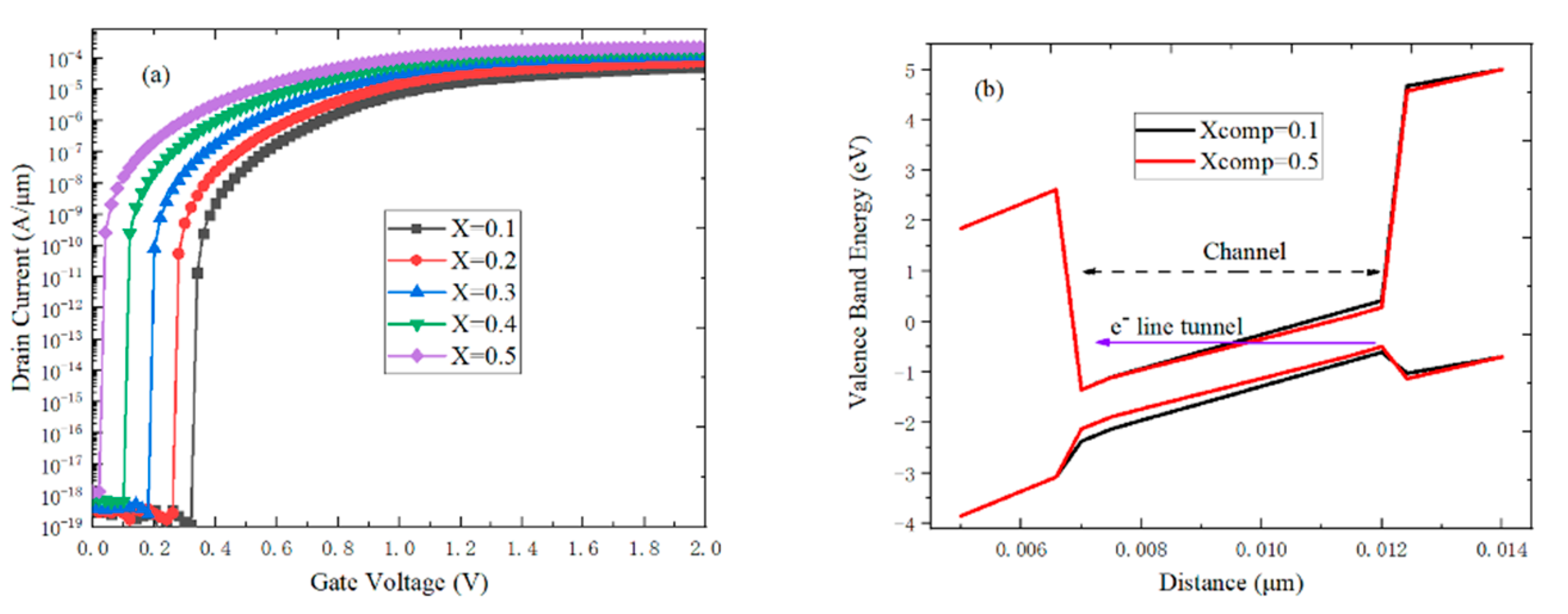
Figure 7 shows the effect of Ge content on the performance of the H-DLTFET. In
Figure 7a, the on-state current of the H-DLTFET increased from 52.7 to 222.3 μA/μm, and the transfer characteristic curve drifted to the left when the Ge content increased from 0.1 to 0.5. The Ge content had an influence on the forbidden bandwidth of Si
1-xGe
x material and on the tunneling barrier width between the source and the channel. It can also be explained by the on-state energy band from the top of the channel to the bottom of the channel according to the different Ge content, as shown in
Figure 7b. The energy band became steeper and the electric field and line tunneling area become higher as the Ge content increased, which increased the on-state current. Therefore, the optimum Ge content was 0.4.
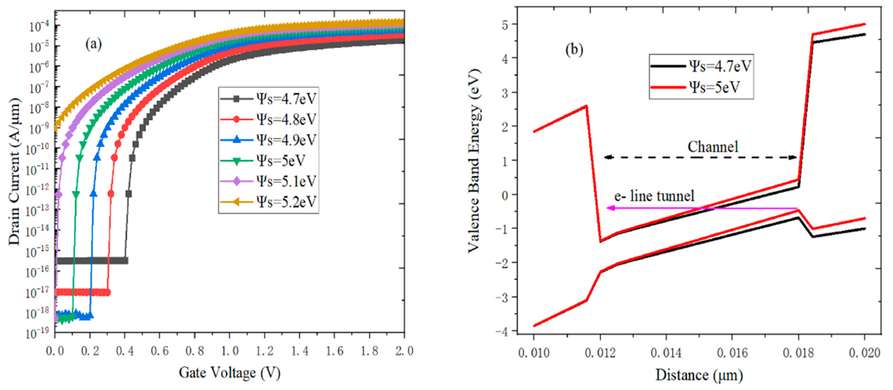
Finally, the influence of the source work function (Ψ
s) on the performance of H-DLTFETs was also studied. As shown in
Figure 8a, the on-state current increased from 19.9 to 110.7 μA/μm when Ψ
s increased from 4.7 to 5.1 eV, so the optimal Ψ
s was 5 eV. At the same time, the off-state current decreased by more than three orders of magnitude. The pseudo-mutation PN junction became steeper, the electric field became higher, and more holes accumulated at the bottom of the channel when the Ψ
s became larger, so the line tunneling current was higher. As shown in
Figure 8b, the on-state energy band and electron thermal excitation barrier at the bottom of the channel became steeper and larger as the Ψ
s increased, and the off-state leakage current could be suppressed effectively.
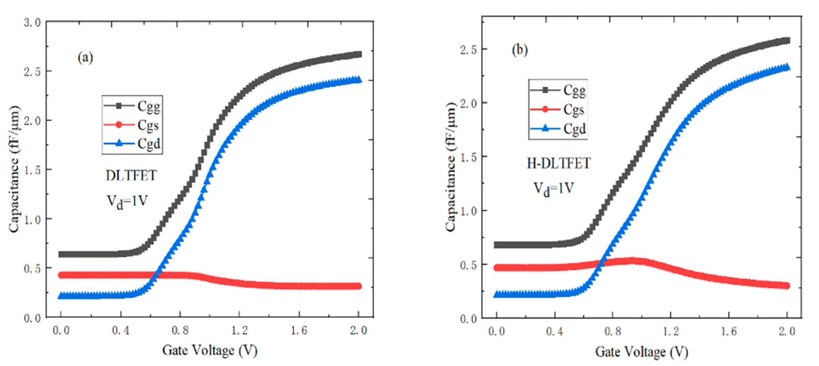
3.4. Capacitance Characteristics
The gate capacitance (
Cgg) is one of the basic parameters used to evaluate the frequency characteristic and analog/RF performance of DLTFETs and H-DLTFETs.
Cgg is mainly composed of gate-drain capacitance (
Cgd) and gate-source capacitance (
Cgs) [
31]. TFETs have a small
Cgs due to the presence of the source/channel tunneling junction.
Figure 9a,b shows the capacitance characteristics of the DLTFET and the H-DLTFET.
Cgg and
Cgd both increased as the
Vgs increased, and C
gs maintained a very small value when the drain voltage was 1 V. Therefore,
Cgd was the major component of
Cgg. It can be seen in
Figure 9a,b that
Cgg and
Cgd of the H-DLTFET were slightly lower than that of the DLTFET. The electrons of the source/channel tunneling junction were collected by the drain region. Due to the Ge–Si heterojunction, the electric field at the tunneling junction of the H-DLTFET was higher than that of the DLTFET. Meanwhile, the electron tunneling rate changed as the gate voltage changed, which could also lead to a rapid change in the accumulated electrons.
3.5. Frequency Characteristic
The cutoff frequency (
fT) and
GBW product are important indicators for evaluating the frequency characteristics of DLTFETs and H-DLTFETs [
32]. In Equation (2), the f
T can be expressed by a ratio of
gm to
Cgg [
33,
34].
The
GBW can be expressed as a ratio of
gm to
Cgd for the DC gain value equal to 10 [
35], as shown in Equation (3).
Figure 10a,b shows the
fT and
GBW of the DLTFET and H-DLTFET when the drain voltage was 1 V. The DLTFET could achieve a maximum
fT of 7.95 GHz and a maximum
GBW of 1.12 GHz when
Vg = 0.9 V and
Vgs = 0.88 V, respectively. However, the maximum
fT of 20.75 GHz and the maximum
GBW of 2.71 GHz of the H-DLTFET could be achieved when
Vgs = 0.94 V and
Vgs = 0.86 V. Therefore, the H-DLTFET showed better analog/RF performance, so it can be used for the health Internet of Things (IOTs) applications.
4. Conclusions
In this paper, a H-DLTFET is proposed and studied using TCAD simulation. Unlike conventional DLTFETs, the source and channel regions of the H-DLTFET used Ge and Si0.6Ge0.4 materials to obtain a higher carrier mobility and a lower tunneling barrier width. The energy band and the carrier tunneling efficiency of the tunneling junction became steeper and higher because of the Si0.6Ge0.4 heterojunction between the source and the channel, which could greatly improve the on/off current ratio and frequency characteristics. In addition, the effects of the source work function, gate oxide dielectric thickness, and Ge content on the performance of the H-DLTFET were analyzed in detail, and then, the above optimal device parameters were obtained. The simulation results showed that the on-state current and the output saturation drain current of the H-DLTFET increased from 83 and 83.5 to 169 and 166.9 μA/μm, respectively. The maximum gm also increased from 81.5 to 198.8 μS/μm, and the switching ratio increased by three orders of magnitude compared with the DLTFET when Vd = 1 V and Vg = 2 V. The average SS and minimum SS of the DLTFET were 26.7 mV/Dec and 6.7 mV/Dec, respectively, whereas the average SS and minimum SS of the H-DLTFET were 15.2 mV/Dec and 3.9 mV/Dec, respectively. Meanwhile, the fT and GBW of the H-DLTFET increased from 7.95 and 1.12 to 20.75 and 2.71 GHz, respectively. Therefore, the H-DLTFET had a higher switching ratio and better analog/RF performance, and it has great potential for use in the Internet of Things and neural network computers.
Author Contributions
Conceptualization and writing—original draft preparation, T.H.; methodology, S.W.; validation, S.C.; writing—review and editing, H.L. and W.L.; funding acquisition, H.L.
Funding
This research was funded by the National Natural Science Foundation of China (Grant No. U1866212), the Foundation for Fundamental Research of China (Grant No. JSZL2016110B003), the Major Fundamental Research Program of Shaanxi (Grant No. 2017ZDJC-26), the Innovation Foundation of Radiation Application (Grant No.KFZC2018040206), and the Fundamental Research Funds for the Central Universities (Grant No. 20101196741). It was also supported by the Shanghai Aerospace Science and Technology Innovation Fund, the Fundamental Research Funds for the Central Universities, and the Innovation Fund of Xidian University.
Conflicts of Interest
The authors declare no conflicts of interest.
References
- Yadav, S.; Sharma, D. Assessment of read and write stability for 6T SRAM cell based on charge plasma DLTFET. Superlattices Microstruct. 2018, 115, 67–77. [Google Scholar] [CrossRef]
- Krishnamohan, T.; Kim, D.; Raghunathan, S.; Saraswat, K. Double-Gate Strained-Ge Heterostructure Tunneling FET (TFET) with record high drive currents and 60 mV/dec subthreshold slope. In Proceedings of the IEEE International Electron Devices Meeting, San Francisco, CA, USA, 15–17 December 2008; pp. 1–3. [Google Scholar] [CrossRef]
- Lattanzio, L.; De Michielis, L.; Ionescu, A.M. Complementary germanium electron–hole bilayer tunnel FET for sub-0.5-V operation. IEEE Electron Device Lett. 2012, 33, 167–169. [Google Scholar] [CrossRef]
- Dash, S.; Mishra, G.P. A new analytical threshold voltage model of cylindrical gate tunnel FET (CG-TFET). Superlattices Microstruct. 2015, 86, 211–220. [Google Scholar] [CrossRef]
- Chauhan, S.S.; Sharma, N. Impact of Spacer-Gate Engineered Workfunction on the Performance of Dopingless TFET. J. Nanoelectron. Optoelectron. 2018, 13, 1200–1203. [Google Scholar] [CrossRef]
- Lee, Y.; Kwon, J.; Hwang, E.; Ra, C.H.; Yoo, W.J.; Ahn, J.H.; Park, J.H.; Cho, J.H. High-performance perovskite–graphene hybrid photodetector. Adv. Mater. 2015, 27, 41–46. [Google Scholar] [CrossRef]
- Xu, J.; Jia, J.; Lai, S.; Ju, J.; Lee, S. Tunneling field effect transistor integrated with black phosphorus-MoS2 junction and ion gel dielectric. Appl. Phys. Lett. 2017, 110, 033103. [Google Scholar] [CrossRef]
- Oyedele, A.D.; Yang, S.; Liang, L.; Puretzky, A.A.; Wang, K.; Zhang, J.; Yu, P.; Pudasaini, P.R.; Ghosh, A.W.; Liu, Z.; et al. PdSe2: Pentagonal two-dimensional layers with high air stability for electronics. J. Am. Chem. Soc. 2017, 139, 14090–14097. [Google Scholar] [CrossRef] [PubMed]
- Damrongplasit, N.; Kim, S.H.; Liu, T.J.K. Study of random dopant fluctuation induced variability in the raised-Ge-source TFET. IEEE Electron Device Lett. 2013, 34, 184–186. [Google Scholar] [CrossRef]
- Cristoloveanu, S.; Athanasiou, S.; Bawedin, M.; Galy, P. Evidence of supercoupling effect in ultrathin silicon layers using a four-gate MOSFET. IEEE Electron Device Lett. 2017, 38, 157–159. [Google Scholar] [CrossRef]
- Guerfi, Y.; Larrieu, G. Vertical silicon nanowire field effect transistors with nanoscale gate-all-around. Nanoscale Res. Lett. 2016, 11, 210. [Google Scholar] [CrossRef] [PubMed]
- Rigante, S.; Scarbolo, P.; Wipf, M.; Stoop, R.L.; Bedner, K.; Buitrago, E.; Bazigos, A.; Bouvet, D.; Calame, M.; Schönenberger, C.; Ionescu, A.M. Sensing with advanced computing technology: Fin field-effect transistors with high-k gate stack on bulk silicon. ACS Nano 2015, 9, 4872–4881. [Google Scholar] [CrossRef] [PubMed]
- Raad, B.R.; Nigam, K.; Sharma, D.; Kondekar, P.N. Performance investigation of bandgap, gate material work function and gate dielectric engineered TFET with device reliability improvement. Superlattices Microstruct. 2016, 94, 138–146. [Google Scholar] [CrossRef]
- Anand, S.; Sarin, R.K. Gate misalignment effects on analog/RF performance of charge plasma-based doping-less tunnel FET. Appl. Phys. A 2017, 123, 413. [Google Scholar] [CrossRef]
- Choi, W.Y.; Park, B.G.; Lee, J.D.; Liu, T.J.K. Tunneling field-effect transistors (TFETs) with subthreshold swing (SS) less than 60 mV/dec. IEEE Electron Device Lett. 2007, 28, 743–745. [Google Scholar] [CrossRef]
- Raushan, M.A.; Alam, N.; Siddiqui, M.J. Dopingless Tunnel Field-Effect Transistor with Oversized Back Gate: Proposal and Investigation. IEEE Trans. Electron Devices 2018, 99, 1–8. [Google Scholar] [CrossRef]
- Raad, B.; Nigam, K.; Sharma, D.; Kondekar, P. Dielectric and work function engineered TFET for ambipolar suppression and RF performance enhancement. Electron. Lett. 2016, 52, 770–772. [Google Scholar] [CrossRef]
- Cecil, K.; Singh, J. Influence of Germanium source on dopingless tunnel-FET for improved analog/RF performance. Superlattices Microstruct. 2017, 101, 244–252. [Google Scholar] [CrossRef]
- Anand, S.; Sarin, R.K. An analysis on ambipolar reduction techniques for charge plasma based tunnel field effect transistors. J. Nanoelectron. Optoelectron. 2016, 11, 543–550. [Google Scholar] [CrossRef]
- Revelant, A.; Villalon, A.; Wu, Y.; Zaslavsky, A.; Iwai, H.; Cristoloveanu, S. Electron-hole bilayer TFET: Experiments and comments. IEEE Trans. Electron Devices 2014, 61, 2674–2681. [Google Scholar] [CrossRef]
- Lahgere, A.; Panchore, M.; Singh, J. Dopingless ferroelectric tunnel FET architecture for the improvement of performance of dopingless n-channel tunnel FETs. Superlattices Microstruct. 2016, 96, 16–25. [Google Scholar] [CrossRef]
- Bagga, N.; Sarkar, S.K. An analytical model for tunnel barrier modulation in triple metal double gate TFET. IEEE Trans. Electron Devices 2015, 62, 2136–2142. [Google Scholar] [CrossRef]
- Anand, S.; Amin, S.I.; Sarin, R.K. Analog performance investigation of dual electrode based doping-less tunnel FET. J. Comput. Electron. 2016, 15, 94–103. [Google Scholar] [CrossRef]
- Kumar, M.J.; Janardhanan, S. Doping-less tunnel field effect transistor: Design and investigation. IEEE Trans. Electron Devices 2013, 60, 3285–3290. [Google Scholar] [CrossRef]
- Sharma, N.; Chauhan, S.S. Dual metal drain Ge-source dopingless TFET with enhanced turn-ON steep subthreshold swing and high ON-current. Electron. Lett. 2017, 53, 960–962. [Google Scholar] [CrossRef]
- Villalon, A.; Le Carval, G.; Martinie, S.; Le Royer, C.; Jaud, M.A.; Cristoloveanu, S. Further insights in TFET operation. IEEE Trans. Electron Devices 2014, 61, 2893–2898. [Google Scholar] [CrossRef]
- Sharma, A.; Goud, A.A.; Roy, K. GaSb-InAs n-TFET with doped source underlap exhibiting low subthreshold swing at sub-10-nm gate-lengths. IEEE Electron Device Lett. 2014, 35, 1221–1223. [Google Scholar] [CrossRef]
- Anand, S.; Amin, S.I.; Sarin, R.K. Performance analysis of charge plasma based dual electrode tunnel FET. J. Semicond. 2016, 37, 054003. [Google Scholar] [CrossRef]
- Naik, V.; Chauhan, S.S. Si0.5Ge0.5 Single and Hetero-gate dielectric doping-less tunnel FETs. In Proceedings of the IEEE International Conference on Communication and Signal Processing (ICCSP), Melmaruvathur, India, 6–8 April 2016; pp. 0635–0638. [Google Scholar] [CrossRef]
- Padilla, J.L.; Alper, C.; Gámiz, F.; Lonescu, A.M. Assessment of field-induced quantum confinement in heterogate germanium electron–hole bilayer tunnel field-effect transistor. Appl. Phys. Lett. 2014, 105, 082108. [Google Scholar] [CrossRef]
- Anand, S.; Sarin, R.K. Dual material gate doping-less tunnel FET with hetero gate dielectric for enhancement of analog/RF performance. J. Semicond. 2017, 38, 024001. [Google Scholar] [CrossRef]
- Singh, D.; Pandey, S.; Nigam, K.; Sharma, D.; Yadav, D.S.; Kondekar, P. A charge-plasma-based dielectric-modulated junctionless TFET for biosensor label-free detection. IEEE Trans. Electron Devices 2017, 64, 271–278. [Google Scholar] [CrossRef]
- Lattanzio, L.; De Michielis, L.; lonescu, A.M. The electron–hole bilayer tunnel FET. Solid-State Electron. 2012, 74, 85–90. [Google Scholar] [CrossRef]
- Padilla, J.L.; Alper, C.; Medina-Bailón, C.; Gámiz, F.; lonescu, A.M. Assessment of pseudo-bilayer structures in the heterogate germanium electron-hole bilayer tunnel field-effect transistor. Appl. Phys. Lett. 2015, 106, 262102. [Google Scholar] [CrossRef] [Green Version]
- Juyal, R.; Chauhan, S.S. TCAD simulation of germanium source dopingless tunnel FET. In Proceedings of the IEEE International Conference on Advances in Computing, Communication, & Automation (ICACCA), Dehradun, India, 8–9 April 2016; pp. 1–3. [Google Scholar] [CrossRef]
© 2019 by the authors. Licensee MDPI, Basel, Switzerland. This article is an open access article distributed under the terms and conditions of the Creative Commons Attribution (CC BY) license (http://creativecommons.org/licenses/by/4.0/).


