Unit-Cell-Based Domain Decomposition Method for Efficient Simulation of a Truncated Electromagnetic Bandgap Structure in High-Speed PCBs


Department of Electrical, Electronic, and Control Engineering, and the Institute for Information Technology Convergence, Hankyong National University, Anseong 17579, Korea
Electronics 2018, 7(9), 201; https://doi.org/10.3390/electronics7090201
Submission received: 19 August 2018
/
Revised: 11 September 2018
/
Accepted: 14 September 2018
/
Published: 17 September 2018
Abstract
:In this paper, we present a unit-cell-based domain decomposition method (UC-DDM) for rapid and accurate simulation of predicting the parallel plate noise (PPN) suppression of a truncated electromagnetic bandgap (EBG) structure in high-speed printed circuit boards (PCBs). The proposed UC-DDM divides the analysis domain of the truncated EBG structure into UCs as sub-domains. Solving a sub-domain is based on a novel UC model, yielding an analytical expression for the impedance parameter (Z-parameter) of the UC. The novel UC model is derived using a spatial decomposition technique, which results in the modal decomposition of quasi-transverse electromagnetic (TEM) and transverse magnetic (TM) modes. In addition, we analytically derive a impedance-parameter recombination method (ZRM) to obtain the analytical solution of a finite EBG array from the sub-domain results. The proposed UC-DDM is verified through comparison with full-wave simulation results for various EBG arrays. Comparison between the UC-DDM and a full-wave simulation of a truncated EBG structure reveals that a substantial improvement in computation time with high accuracy is achieved. It is demonstrated that the simulation time of the proposed method is only 0.1% of that of a full-wave simulation without accuracy degradation.
1. Introduction
Parallel plate noise (PPN) is a critical design consideration for high-speed printed circuit boards (PCBs). As processor clock speeds and device-to-device communication speeds dramatically increase, wideband PPN causes more serious problems of signal integrity (SI), power integrity (PI), and electromagnetic interference (EMI) in high-speed PCBs [1,2,3]. The PPN not only induces noisy power supply with voltage fluctuation, but also low digital signal quality with waveform distortion. The PPN severely interferes with radio frequency (RF) signals, which results in connection failure of wireless communication systems. Moreover, the PPN is coupled with the cables attached to high-speed PCBs and consequently causes a problem of common-mode noise radiation [4]. In particular, the power distribution networks of high-speed PCBs mainly contribute to the generation and propagation of PPN, because the parallel plate modes of power distribution networks are easily excited by digital switching devices and the power distribution network is shared by various chips on a board. As a consequence, it is imperative that the PPN of a power distribution network is suppressed to ensure good SI, PI, and EMI characteristics of high-speed PCBs.
To mitigate the PPN of a power distribution network in high-speed PCBs, electromagnetic bandgap (EBG) structures have been proposed. The EBG structures have been intensively studied due to their superior characteristics of PPN suppression in high-speed PCBs [5,6,7,8,9,10,11,12,13,14,15,16,17]. In the EBG structures, the conductors of a power distribution network are etched in specific patterns, which are equivalently considered as resonant circuits to filter out the PPN in high-speed PCBs. In [5], the metallo-dielectric EBG structure forms a resonator consisting of an inductor and a capacitor in series, namely a LC resonator. The EBG structure shows PPN suppression of a parallel plate waveguide, which is typically used as a power distribution network. Based on the initial EBG structure, research on improving the EBG structure has been conducted intensively, as reported in [6,7,8,9,10,11,12,13,14,15,16,17,18]. To widen the bandwidth of the PPN suppression, various techniques, such as vertically stacked patches, multiple vias, and a high dielectric constant material have been presented [6,7,8,9,10,11,12,13,14,15]. For further improvement in size reduction as well as noise suppression bandwidth, a perforated plane (PP) has been employed [16,17,18]. As can be seen in previous research, the EBG structures achieve excellent PPN suppression with the advantage of high-level suppression over a wideband frequency range. Additionally, the planar structure provides ease of integration with other components and reliable fabrication in a conventional PCB process. Thus, the EBG structures can be an alternative to a conventional power distribution network.
In the EBG structure’s design, estimation of PPN suppression is important. The characteristics of PPN suppression in EBG structures are mainly predicted by dispersion analysis based on the Floquet theory [19,20], or scattering parameters (S-parameters) obtained by electromagnetic (EM) simulations. In the dispersion analysis with the Floquet theory, a dispersion diagram is employed to obtain the stopband of a periodic EBG structure. The dispersion diagram is acquired using a network parameter of the unit cell (UC) rather than the full array of EBG. The network parameters, such as ABCD matrices and impedance parameters (Z-parameters), are extracted from an analytical equation or an equivalent circuit of the UC. The dispersion analysis rapidly predicts the PPN suppression of the periodic EBG structure. Its accuracy is, however, limited to a periodic structure, namely the EBG structure containing an infinite array, because of the periodicity assumption in the Floquet theory. In most applications, the number of the EBG cells is finite and even small. Accordingly, the dispersion analysis is not sufficient for the practical design of a truncated EBG structure suppressing PPN in high-speed PCBs.
The other method is a full-wave EM simulation based on the finite element method (FEM), method of moment (MoM), and finite difference method (FDTD). In full-wave simulations, a finite array of the EBG structure is analyzed so that the network parameters, such as S-parameters, are obtained to estimate PPN suppression. The full-wave simulation does not require a periodic boundary condition. Instead, the array size directly used in applications is examined. The full-wave simulation results provide the S-parameters with the level of PPN suppression. Moreover, it shows resonance peaks below and above the PPN suppression region. Thus, the full-wave simulation is preferred in practical design. However, the computational inefficiency of the full-wave simulation is troublesome. In particular, it is more problematic in the design of a truncated EBG structure using the perforated plane technique (PP-EBG). The PP-EBG structure shows distinguished features of a substantial increase in noise suppression bandwidth, size reduction, low cost, and high reliability—thus, using the PP-EBG structure is highly advantageous for high-speed PCB design. Nevertheless, the design and optimization of a truncated PP-EBG structure using full-wave simulation is time-consuming compared to the other EBG structure without the PP technique, because the field distributions of the PP-EBG structure are not confined within the dielectric material between two conducting layers and the enlargement of the field analysis region results in a significant amount of meshes for EM simulations. Consequently, a simulation method of a truncated PP-EBG structure is needed.
In this paper, we propose an efficient simulation method to predict the PPN suppression of a truncated EBG structure, improved on by the perforated plane technique in high-speed PCBs. The proposed method presents an analytical model of the EBG UC, and an impedance-parameter recombination method (ZRM) to obtain the S-parameters of a truncated PP-EBG structure containing a M-by-N (M × N) array. Modal decomposition into a transmission line mode and resonant cavity mode is developed for the physics-based model of an EBG UC. Additionally, we derive an analytical approach of ZRM to concatenate two adjacent UCs where multiple ports are two-dimensionally (2-D) arranged. Iterative use of ZRM enables us to acquire the network parameters of the M × N array using those of a UC. The proposed method is verified through comparison with full-wave simulation results for various size arrays of the truncated PP-EBG structure. The proposed method significantly reduces the simulation time, thus proving to be an efficient design and a step towards optimization of the PP-EBG structure in high-speed PCBs.
2. Method
2.1. A Procedure of Proposed UC-DDM
The PP-EBG structure was devised based on the multilayer PCBs, which contained at least three metal layers—namely, a perforated plane, a rectangular patch connecting to the perforated plane through a via, and a non-perforated plane. For the application of the PP-EBG structure to a power distribution network, a perforated and non-perforated plane could be used as the power and ground planes, respectively. As described in [16,17], the PP-EBG structure substantially improves the PPN suppression characteristics by simply and cost-effectively increasing characteristic impedance, which can be defined in the equivalent circuit model of the UC. In contrast, using the perforated plane technique is computationally expensive when predicting the noise-suppression characteristics compared to the conventional EBG structure with electromagnetic fields confined between parallel plates. As shown in Figure 1, examples of the PP-EBG structure with a 2 × 2 array and the description of a UC are illustrated. The design parameters for the PP-EBG UC are also shown in Figure 1, and are as follows: The lengths of the UC and the rectangular patch are dC and dr; the perforation size is dP; the distance between the perforated plane and the rectangular patch is h1; the distance between the rectangular patch and the nonperforated plane is h2; and the via radius is r.
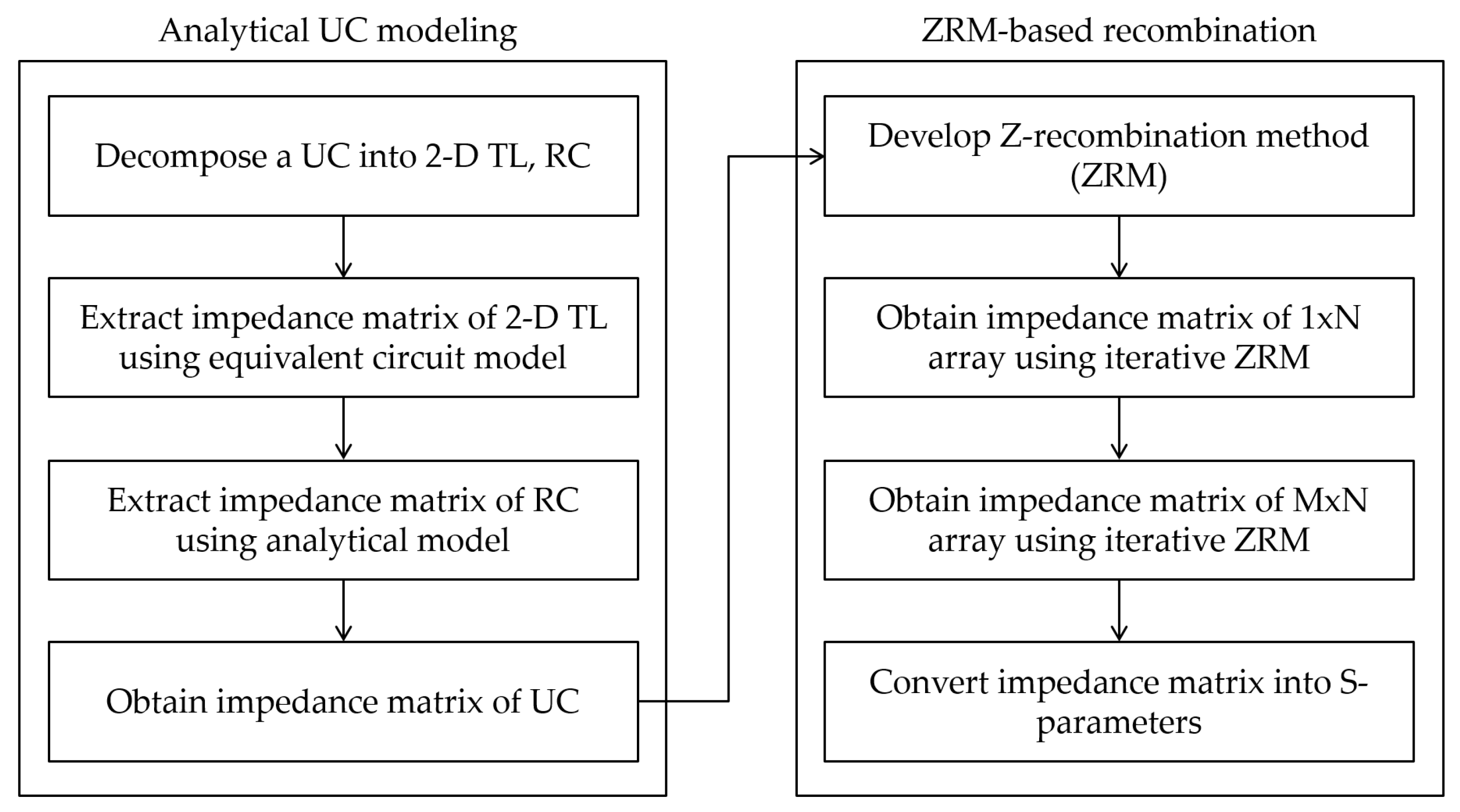
Because the truncated PP-EBG array did not satisfy the periodic boundary condition, the Bloch wave propagation was not defined and the Floquet theory was also not assumed. The proposed UC-DDM was exploited to rapidly and accurately predict the PPN suppression characteristics of the PP-EBG structure containing a finite and small number of UCs. As can be seen in Figure 2, the proposed UC-DDM consisted of two main parts: analytical UC modeling and ZRM. The first part was to derive an analytical UC model in order to extract a Z-parameter of the UC. The second was to perform the UC-DDM using a consecutive application of the impedance-matrix recombination method (ZRM) to obtain the S-parameter of the PP-EBG structure with an M × N array. In the first step, a novel expression for the Z-parameter of the UC was derived using spatial decomposition, which results from the skin effect for the multilayer PCBs. To refine the PP-EBG UC model, an electromagnetic wave propagation in the UC was decomposed into a 2-D transmission line (2-D TL) and a rectangular cavity (RC). The Z-parameters for 2-D TL and RC were analytically extracted. The PP-EBG UC model was given by combining the characteristics of 2-D TL and RC. The next main part is the UC-DDM using ZRM, where the S-parameters of the truncated PP-EBG structure were obtained by continuously applying the ZRM based on the analytical expression for the Z-parameter of the UC, which was derived in the first step. The analysis domain for a truncated EBG structure was divided into sub-domains corresponding to the UCs. The solution for a sub-domain was given by the analytical UC model. ZRM is the method used to simply and analytically provide the Z-parameter of the new EBG array merged by two different or identical structures. The iterative use of ZRM consequently results in the solution of the original domain, namely the PPN suppression characteristics of the truncated EBG structure.
2.2. Analytical UC Modeling
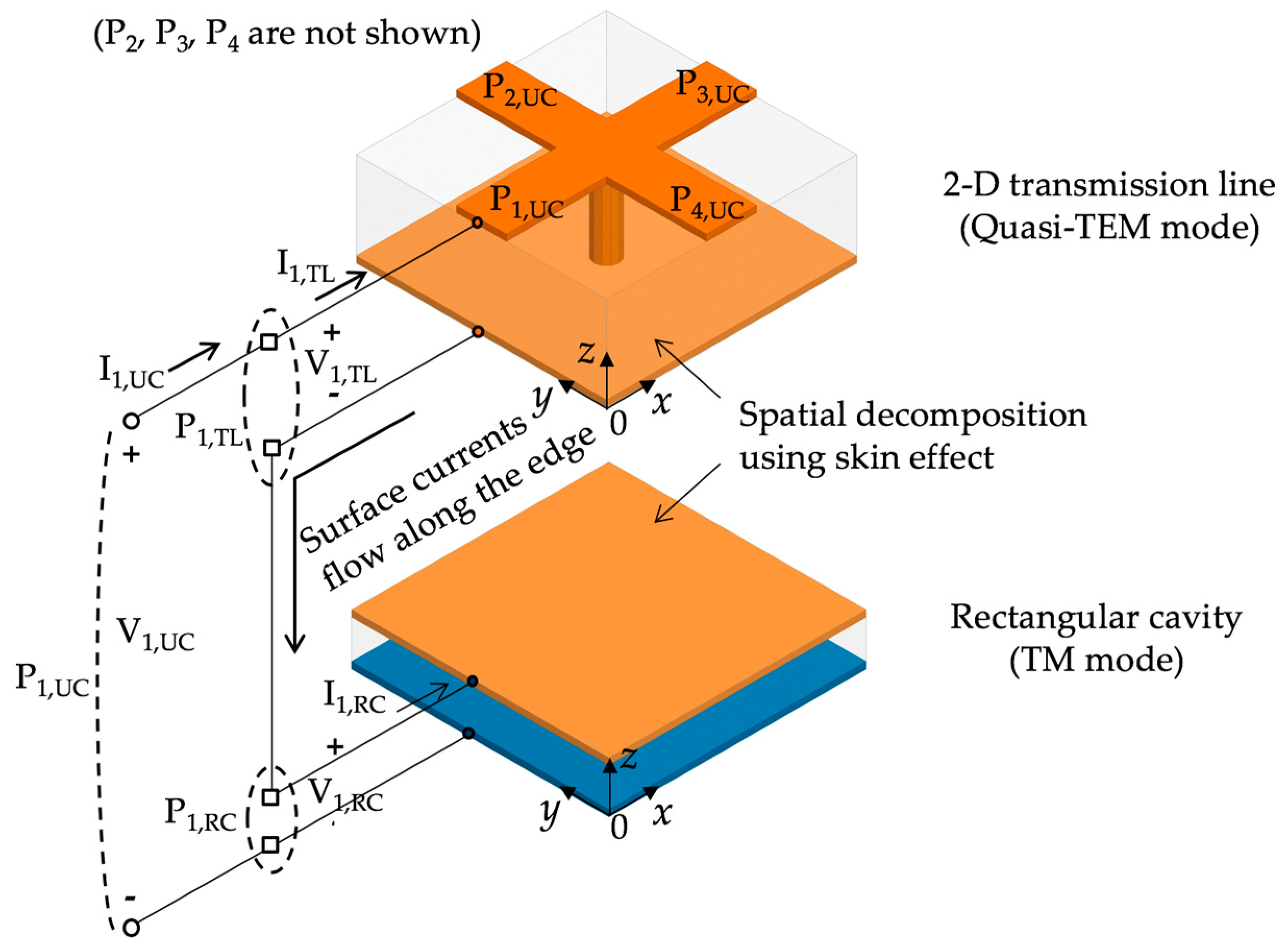
In the proposed UC-DDM, the sub-domain for the analysis of the finite EBG array was based on the UC. For a computationally efficient simulation, the analytical expressions for the Z-parameter of the UC are derived in this section. For a refined model, the spatial decomposition technique for the analytical UC model is presented. In the proposed model, it is assumed that the skin depth in the frequency of interest is typically less than the thickness of a metal plan. This assumption is typically valid in conventional multilayer PCBs where the PP-EBG structure is implemented. For instance, the skin depth at a frequency of 100 MHz is 6 μm for the FR-4-based PCBs, while the copper thickness for the metal layer is approximately 17 μm (i.e., 1/2 oz). Thus, we assumed that most of the return current on a rectangular patch flowed on the surface and detoured at the edge of the patch, instead of penetrating the patch. Based on this assumption, as shown in Figure 3, the UC of the PP-EBG structure is vertically divided into two segments of a 2-D TL and a RC where the dominant modes of the electromagnetic wave propagations are quasi-TEM and TM modes, respectively. One segment of the 2-D TL consists of the perforated plane and the upper parts of the rectangular patch. These are connected to each other at the center position through a single via. The other segment of the RC comprises the lower part of the patch and the nonperforated plane.
For the analytical UC model using spatial decomposition, we defined a port configuration, as shown in Figure 3. The PP-EBG UC as the sub-domain of the UC-DDM contains four original ports. They are represented as P1,UC, P2,UC, P3,UC, and P4,UC. The spatial decomposition generates virtual ports for the 2-D TL and the RC. The virtual ports of the 2-D TL were defined using the terminals located at the perforated plane and the upper rectangular patch, while those of the RC were defined as the terminals on the lower patch and the nonperforated plane, as seen in Figure 3. The notations for port 1 of the 2-D TL and the RC are P1,TL and P1,RC. Note that the other ports are omitted for the sake of simplicity. For the spatial decomposition, Figure 3 shows the relationship between the original port P1,UC and the virtual ports P1,TL, P1,RC. The positive and negative terminals of P1,UC are identical to the positive terminal of P1,TL and the negative terminal of P1,RC. Additionally, it is shown that the negative terminal of P1,TL is directly connected to the positive terminal of P1,RC. From the relationships, we further conclude that the segments are connected in series configuration when we combine the segments into the original UC in the analytical approach. The detailed description will be explained using equivalent circuits at the end of this section.
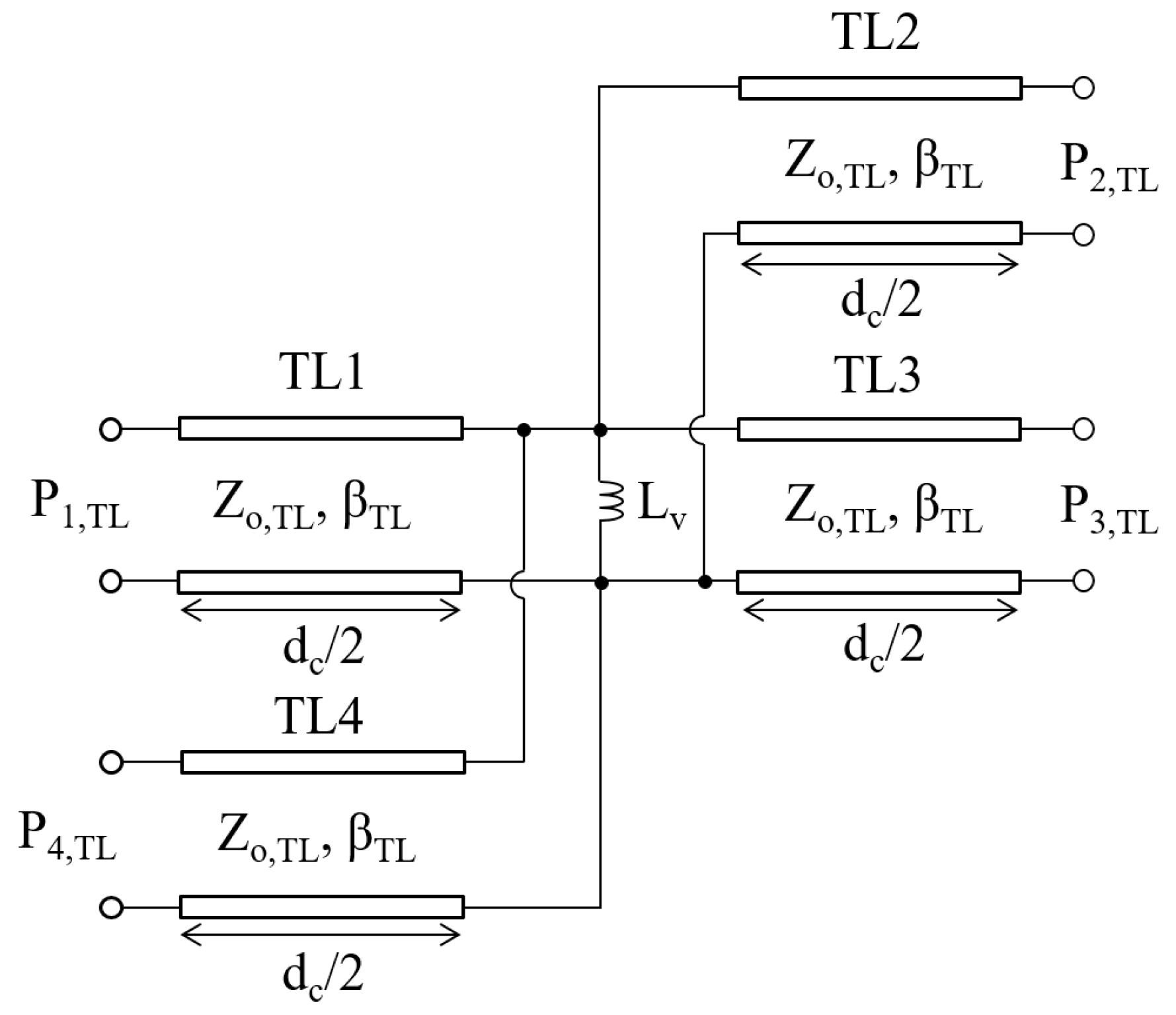
To extract the analytical expressions for the Z-parameter of the 2-D TL segment, the equivalent circuit model was developed as shown in Figure 4. In the model, we adopted four transmission lines with the characteristic impedance Zo,TL, the propagation constant βTL, and the length dC/2. The center via was modeled as an inductor having an inductance value of LV. From the equivalent circuit model, the relationships between voltages and currents are given by:
where
The characteristic impedance Zo,TL can be obtained using the empirically approximated equations [21] in the following:
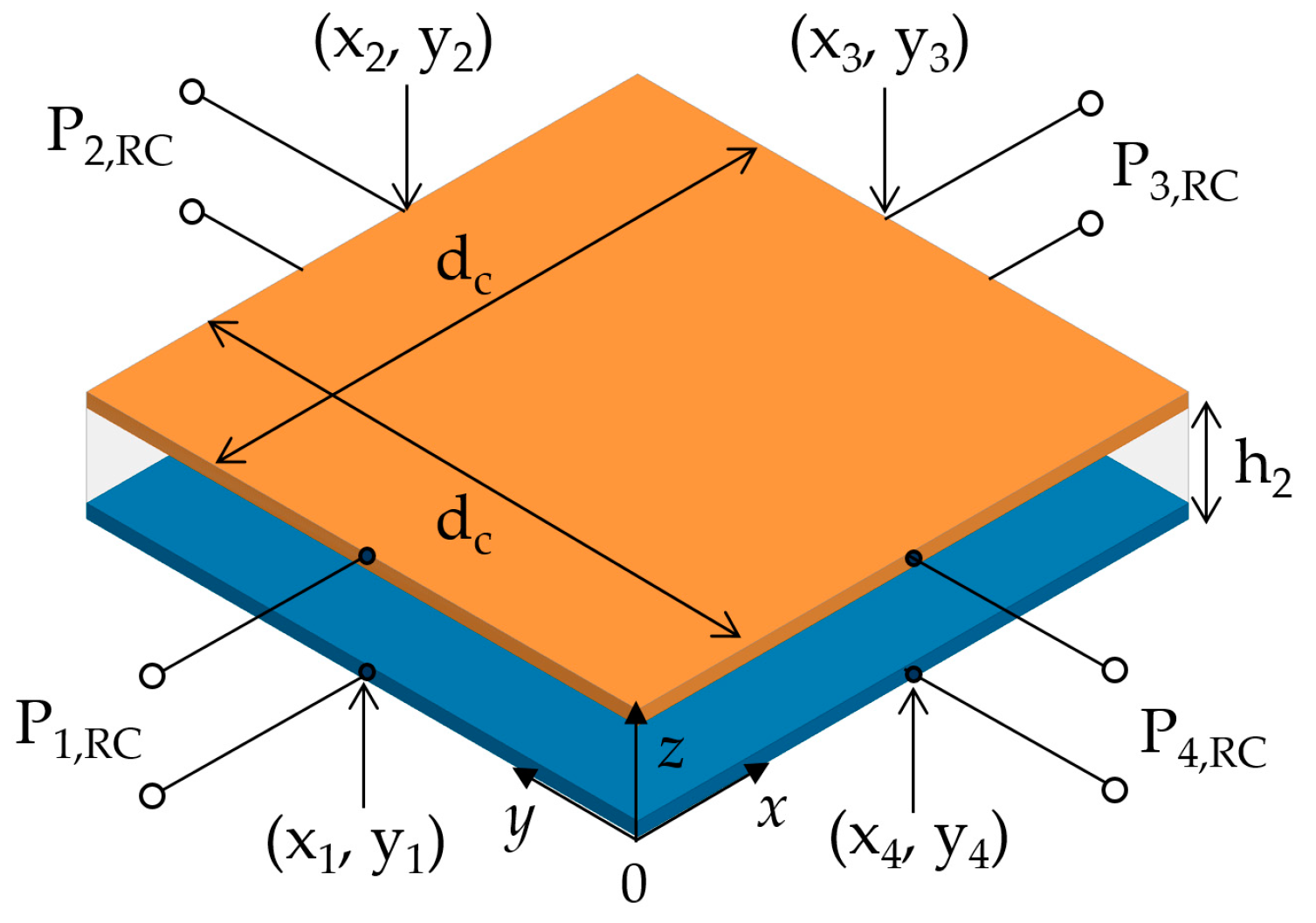
We obtained the analytical expressions for the Z-parameter of the 2-D TL segment. Next, the analytical model of the RC segment was derived using the resonant cavity model in [22]. The resonant cavity model is the analytic wave model providing the Z-parameters of the planar and rectangular cavity implemented in packages and PCBs. Based on the resonant cavity model, the Z-parameter of the RC segment in Figure 5 is given by:
where
Cm = 1 if m = 0 or Cm = if m ≠ 0, and Cn = 1 if n = 0 or Cn = if n ≠ 0. k is a real wave number for a lossless case. The resonant cavity model expresses the Z-parameter of the solution for the Helmholtz eigenvalue problem. Thus, the accuracy increases as the eigenmodes m and n are infinitely summed in the x- and y-directions. However, because this is inefficient for practical applications, we used the approximate approach shown in [21] to determine the mode numbers m and n, rather than the use of an infinite sum. As described in [21], this provides a balance between the level of accuracy and computation time.
An analytical expression for the Z-parameter of the UC was obtained by combining the Z-parameters of the 2-D TL and RC segments. As described previously, the 2D-TL and the RC are electrically connected in series configurations. In Figure 3, the port voltage of the UC is the sum of the voltages of the 2-D TL and the RC segments, while the current continuity condition is fulfilled for the UC and the segments. Consequently, the analytical expression for the Z-parameter of the UC can simply be acquired as follows:
2.3. ZRM-Based Recombination
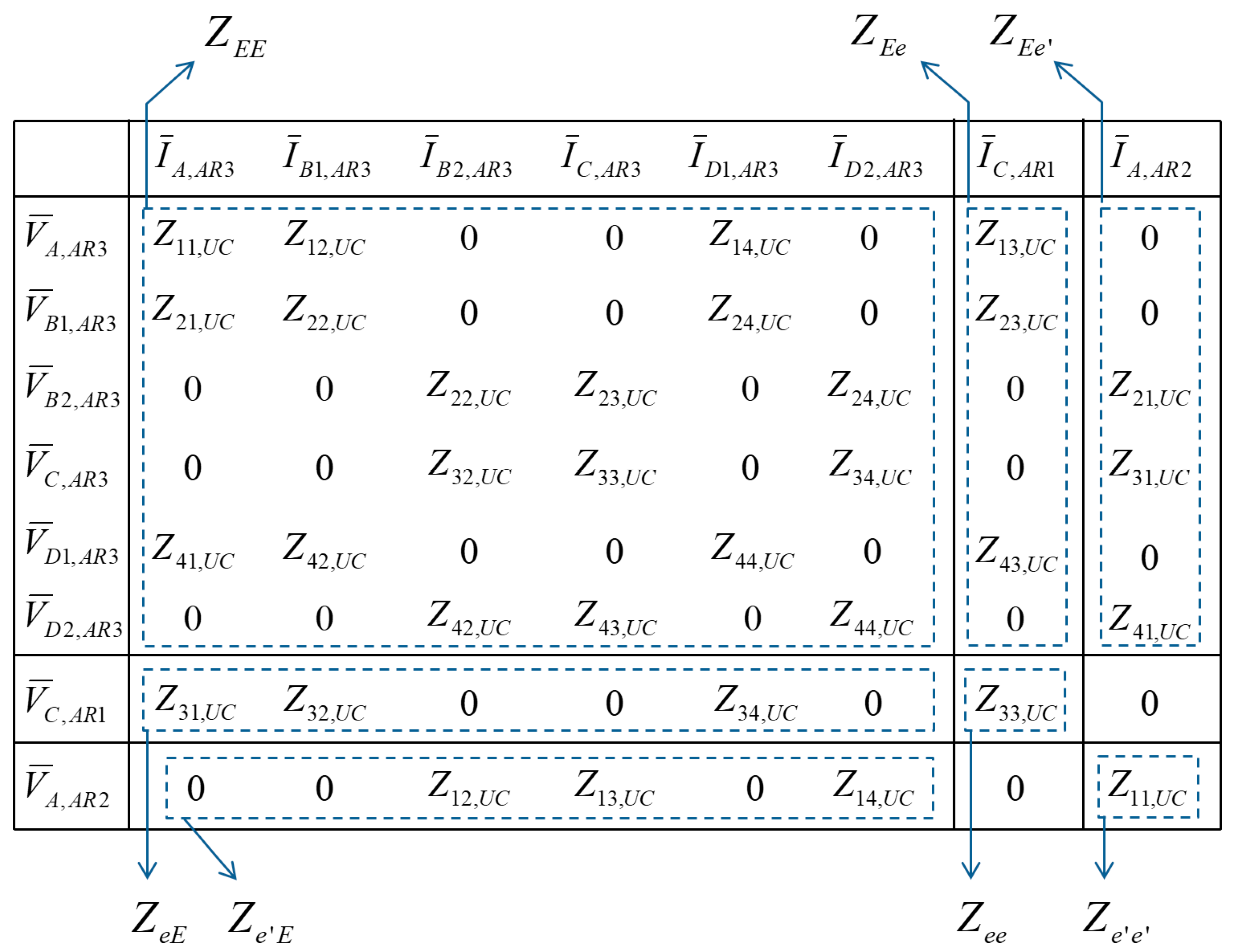
In the proposed UC-DDM, the analysis domain of the original structure is partitioned into the coupled sub-domains of the UCs. The solution of the sub-domain is analytically extracted in the previous section. To reconstruct the original domain using the sub-domain results, a method to recombine the Z-parameters of the sub-domains was developed and named the Z-parameter recombination method (ZRM). Figure 6 depicts a block diagram of two sub-domains to be recombined. The sub-domains are denoted as AR1 and AR2 while the recombined result is denoted as AR3. For convenient application of ZRM to the 2-D truncated EBG array, the multiple ports are arranged in a rectangular order. The sub-domain contains four port groups of PA, PB, PC, and PD. Considering the symmetric nature of the EBG array, we assume the same number of ports q in PA and PC for both AR1 and AR2. In contrast, the port number of PB, PD of AR1 is different from those of AR2 for the general use of ZRM. The port number of PB, PD of AR1 and AR2 is r and s, respectively. The port number of PA, PC of the recombined domain AR3 is the same as those of AR1 or AR2. On the other hand, the port number of PB, PD of AR3 is (r + s), which is the sum of port numbers of AR1 and AR2.
In the proposed UC-DDM, the truncated EBG structure is divided into the UCs by inserting a perfect magnetic conductor (PMC) as a boundary condition. It is shown that the PMC-based decomposition is efficient for the PP-EBG structure in high-speed PCBs. The PMC boundary yields the same voltage and continuous current conditions at the interface between the sub-domains, which is equal to the connection point meeting the port group PC of AR1 with the port group of PA of AR2. With this condition and the segmentation theory introduced in [23], we could derive the Z-parameter of the recombined domain from the Z-parameters of the sub-domains. To utilize the theory in [23] for the ZRM, we created an impedance table showing the relationship between the Z-parameters of the sub-domains and the recombined domain, as shown in Figure 7. In the impedance table of Figure 7, the new Z-parameters of ZEE, ZEe, ZEe′, ZeE, Ze′E, Zee, and Ze′e′ are defined. The Z-parameter of the recombined domain AR3 can thus be obtained by the following:
In the ZRM, a notation ⊕ is newly defined for recombination of the Z-parameters of the sub-domains, as seen above. To show an example of the ZRM, we consider that two UCs are combined into the 1 × 2 EBG array. The Z-parameter of the UC is already found from (1) to (10). Applying the ZRM to two UCs, the Z-parameters in the impedance table is given by:
By substituting the Z-parameters above into (11), the analytical expression for the Z-parameter of the 1 × 2 EBG array is acquired as follows:
where
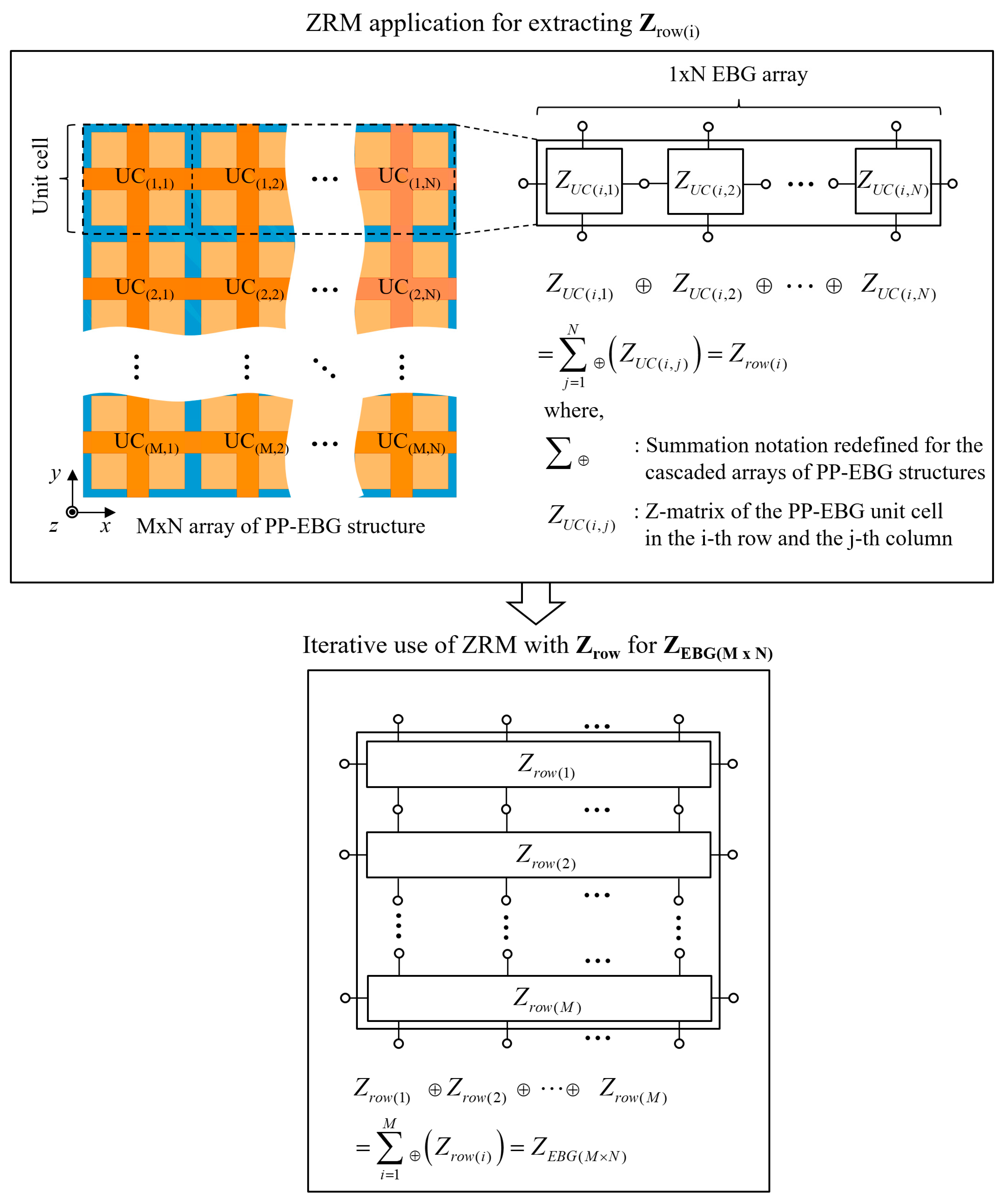
The ZRM for the 1 × 2 array is shown above. To efficiently obtain the Z-parameter of the PP-EBG structure with the M × N array, we iteratively perform the ZRM. The method to iteratively employ the ZRM entails two steps—namely, the ZRM applications for Zrow(i) and ZEBG(M×N). Zrow(i) is the Z-parameter of the 1 × N EBG array, and ZEBG(M×N) is the Z-parameter of the M × N EBG array with the PPN suppression characteristics that we originally needed to examine. In the first step for Zrow(i), we start by recombining two UCs for a 1 × 2 array and the ZRM is sequentially applied to a 1 × N array to obtain Zrow(i). This step is represented as follows:
where ⊕ is the operator of the ZRM.
Next, ZEBG(M×N) is extracted by iteratively performing the ZRM with Zrow(i), as shown in Figure 8. The final ZRM step is given by:
As a consequence, the S-parameter of the truncated EBG structure, showing the PPN suppression, can be calculated as:
where Zo is the reference characteristic impedance, which is typically 50 Ω, and E is the identity matrix. The proposed UC-DDM is clearly described in this section. The UC-DDM is limited to the PP-EBG structure. In particular, there must be a microstrip line of the spatial decomposition to apply the UC-DDM to other EBG structures. However, the ZRM technique, derived herein, can be adopted for other EBG structures when their unit cell models are obtained. The UC-DDM, based on the analytical solutions derived herein, allow engineers to design and optimize the finite-size PP-EBG structure using a code-based approach such as MATLAB, Python, and C language. Moreover, the UC-DDM enables a systematic approach of the PP-EBG structure for practical design in high-speed PCBs.
3. Results
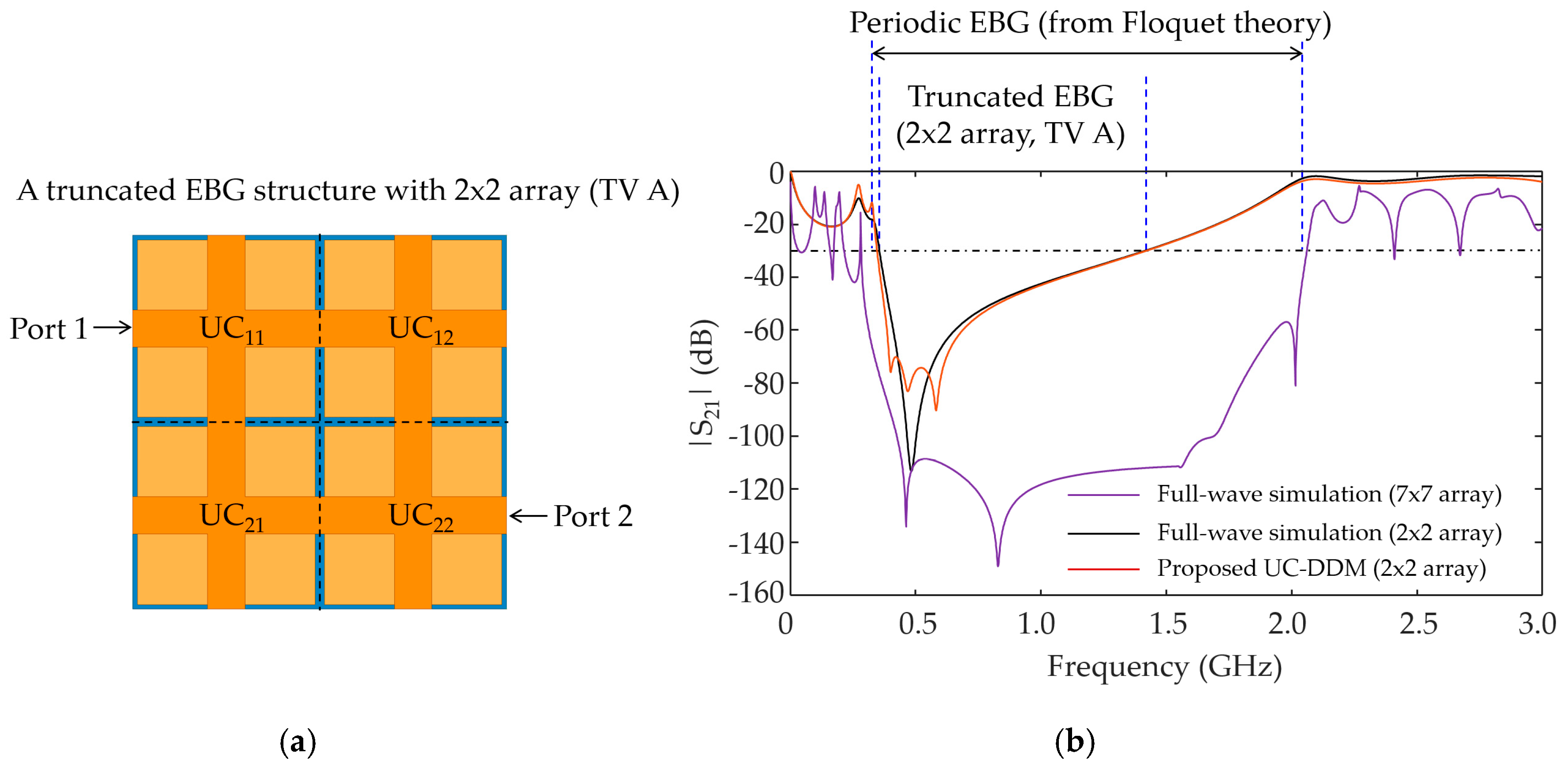
To verify the UC-DDM, we compared the S-parameter results of the UC-DDM for the finite-size array of the PP-EBG structures with those of the FEM simulation. The UC-DDM and the full-wave simulation were implemented using the MATLAB code and modal solution of Ansys HFSS, respectively. Five test vehicles (TVs), including different array size and port positions, were adopted to verify the proposed UC-DDM. The first test vehicle (TV A) was a truncated PP-EBG structure with a 2 × 2 array, as shown in Figure 9. The dimensions of the design parameters used herein were the values typically chosen in the conventional PCB process, where FR-4 and copper were used as the dielectric material and metal layer, respectively. Two dielectric thicknesses, h1 and h2 of the PP-EBG UC, were 1.2 mm and 0.1 mm, respectively. The copper thickness was 17 μm. The UC and the rectangular patch lengths were 20 mm and 19.6 mm, respectively. The via radius r, provided by the conventional PCB process, was 200 μm. The length of the perforated plane was 7 mm. In addition, the configuration of the port location in TV A is given in Figure 9, which is frequently employed for PPN suppression in high-speed PCBs. The dimensions of the design parameters are summarized in Table 1.
In Figure 9, the UC-DDM results for TV A (2 × 2 array) is compared with the full-wave simulation results based on FEM. As can be seen in the figure, the UC-DDM results show good agreement with the FEM simulation results. We define the low and high cut-off frequencies (fL and fH) with the PPN suppression level of −30 dB. fL of the UC-DDM, and the full-wave simulation is 0.35 GHz. fH is 1.42 GHz. In addition to the high correlation of fL and fH, the UC-DDM successfully predicts the PPN suppression over a wideband frequency range. It is verified that the UC-DDM provides accurate results compared to the conventional simulation method. The computation time was examined using a personal computer with an Intel Xeon CPU E3-1505M v5 @ 2.80 GHz. The computation time of the full-wave simulation was 1722 s, whereas the UC-DDM required a computation time of 2.6 s. Remarkably, the simulation time of the UC-DDM is approximately 0.1% of the full-wave simulation time. Using the UC-DDM, rapid and accurate simulation of the truncated PP-EBG structure can be achieved.
On the other hand, the finite-array effect on the reduction of the PPN suppression was also demonstrated. The PPN suppression characteristics of the finite-size array (i.e., 2 × 2) and the infinite array are compared in Figure 9. The result of the infinite array was acquired using a dispersion analysis based on the Floquet theory. Moreover, we show the full-wave simulation result for the 7 × 7 EBG array, which can be considered as an infinite EBG array. It is found in [19,20] that a dispersion analysis based on the Floquet theory shows good prediction of PPN suppression characteristics when the array size is sufficiently large enough to be considered as an infinite array. However, we can observe a significant discrepancy between the PPN suppression characteristics of the 2 × 2 array and infinite array. The predictions of fL and fH of the infinite-array analysis were 0.33 GHz and 2.03 GHz while those of the 2 × 2 array were 0.35 GHz and 1.42 GHz. The periodic analysis based on the Floquet theory shows error of the PPN suppression bandwidth up to 58% compared to the finite array analysis of the UC-DDM and full-wave simulation.
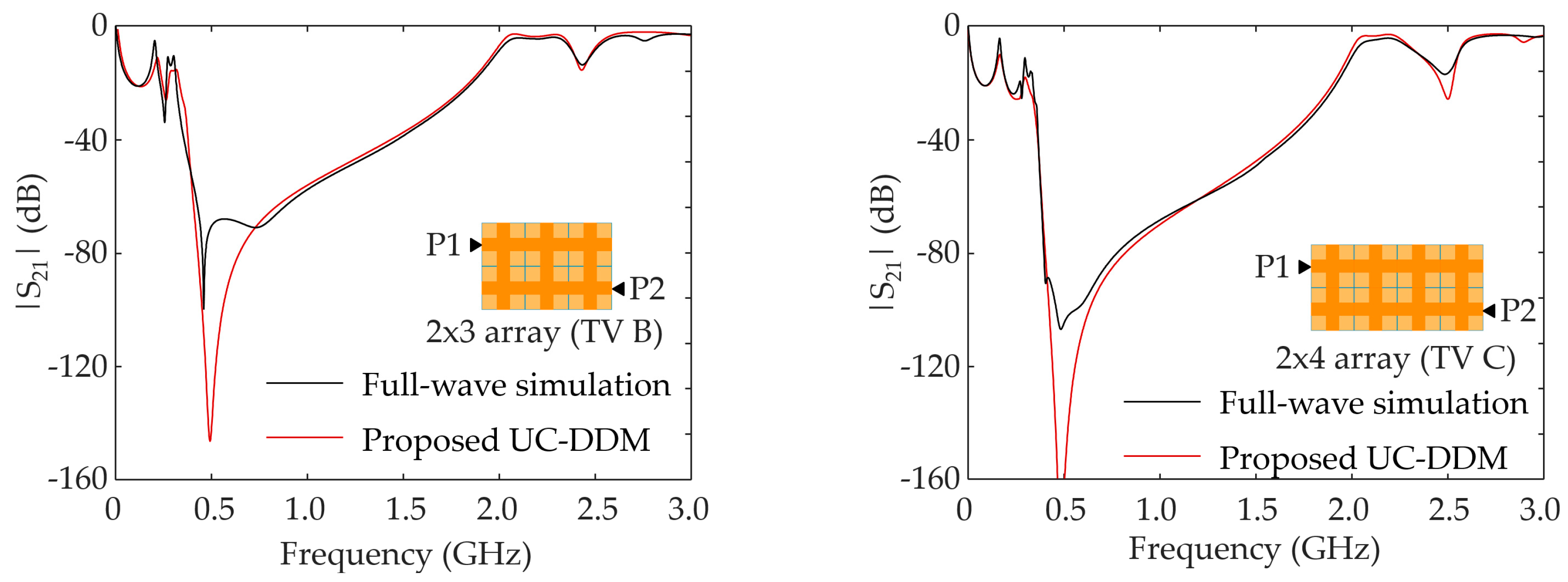
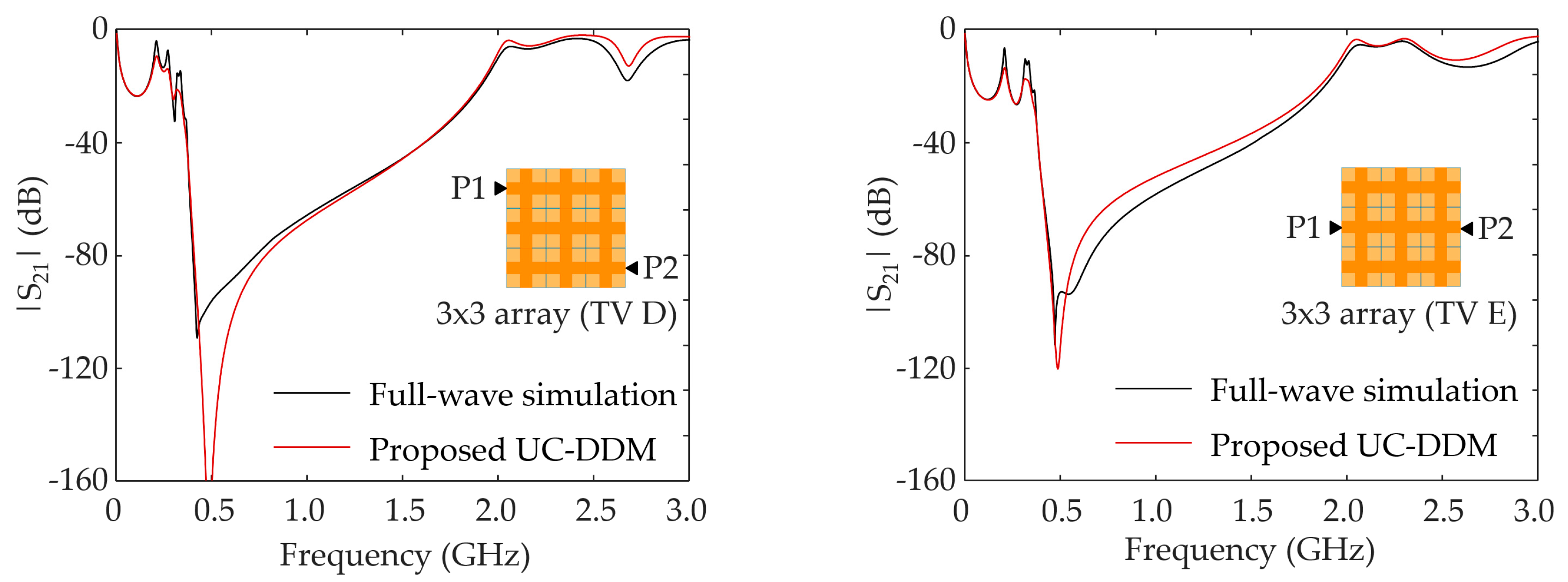
To further validate the UC-DDM, the PPN suppression characteristics (i.e., S21 parameters) were examined using TVs, including different array size and port configurations. As shown in Figure 10, TV B and TV C are PP-EBG structures with 2 × 3 and 2 × 4 arrays, respectively. TV D and TV E contain the same array size of 3 × 3 but different port configurations, as shown in Figure 11. The S21 parameters of TV B (2 × 3 array), TV C (2 × 4 array), and TV D (3 × 3 array) from the full-wave simulation and the UC-DDM are depicted in Figure 10 and Figure 11. The UC-DDM results show good agreement with the full-wave simulation results regardless of the various array sizes. For the different port configurations in Figure 11, the UC-DDM shows good correlation with the full-wave simulation results. Through all TVs, we can observe high accuracy of the UC-DDM regarding prediction of the resonance peaks as well as the PPN suppression bandwidth, thus achieving efficient estimation over a wideband frequency range.
On examination of the computation time, it is shown that the UC-DDM significantly reduced the simulation time for all TVs compared to the full-wave simulation. The simulation times of the full-wave simulation from TV A to TV E are 1722 s, 1931 s, 2937 s, 1905 s, and 1848 s, while those of the proposed UC-DDM are 2.6 s, 2.7 s, 2.8 s, 3.1 s, and 2.9 s. To obtain the PPN suppression characteristics of the truncated EBG structure, the UC-DDM requires approximately 0.1% of the computation time of the full-wave simulation. As a consequence, it is verified that the UC-DDM achieves fast and accurate simulation. These excellent results are summarized in Table 2.
4. Conclusions
We proposed an efficient simulation method based on the UC-DDM for rapid and accurate simulations of the truncated PP-EBG structure in high-speed PCBs. The entire EBG structure with finite array size was divided into smaller nonoverlapping subdomains that were identical to the unit cells. The analytical solution of the UC was derived using a spatial decomposition technique. To combine the UCs, the ZRM was analytically extracted. The analytical UC model and the ZRM improved the simulation of the truncated PP-EBG structure. The accuracy and reduced computation time of the UC-DDM were verified through comparison with the full-wave simulation results for various TVs of the finite PP-EBG structures. A substantial reduction of the computation time using the UC-DDM was also demonstrated. The UC-DDM is a flexible method and can be applied to other EBG structures when the UC model is replaced. Because the UC-DDM is implemented by script-based software, its use can be easily extended to the automation of design combined with various optimization techniques, such as machine learning.
Acknowledgments
This work was supported by the National Research Foundation of Korea (NRF) grant funded by the Korea government (Ministry of Science, ICT & Future Planning) (NRF-2016R1C1B1007123).
Conflicts of Interest
The author declares no conflict of interest.
References
- Wu, T.L.; Buesink, F.; Canavero, F. Overview of Signal Integrity and EMC Design Technologies on PCB: Fundamentals and Latest Progress. IEEE Trans. Electromagn. Compat. 2013, 55, 624–638. [Google Scholar] [Green Version]
- Li, E.P.; Wei, X.C.; Cangellaris, A.C.; Liu, E.X.; Zhang, Y.J.; D’Amore, M.; Kim, J.; Sudo, T. Progress Review of Electromagnetic Compatibility Analysis Technologies for Packages, Printed Circuit Boards, and Novel Interconnects. IEEE Trans. Electromagn. Compat. 2010, 52, 248–265. [Google Scholar]
- Swaminathan, M.; Chung, D.; Grivet-Talocia, S.; Bharath, K.; Laddha, V.; Xie, J. Designing and Modeling for Power Integrity. IEEE Trans. Electromagn. Compat. 2010, 52, 288–310. [Google Scholar] [CrossRef] [Green Version]
- Li, P.J.; Tseng, Y.C.; Cheng, C.H.; Wu, T.L. A Novel Absorptive Common-Mode Filter for Cable Radiation Reduction. IEEE Trans. Compon. Packag. Manuf. Technol. 2017, 7, 511–518. [Google Scholar] [CrossRef]
- Abhari, R.; Eleftheriades, G.V. Metallo-dielectric electromagnetic bandgap structures for suppression and isolation of the parallel-plate noise in high-speed circuits. IEEE Trans. Microw. Theory Tech. 2003, 51, 1629–1639. [Google Scholar] [CrossRef]
- Park, J.; Lu, A.C.W.; Chua, K.M.; Wai, L.L.; Lee, J.; Kim, J. Double-stacked EBG structure for wideband suppression of simultaneous switching noise in LTCC-based SiP applications. IEEE Microw. Wirel. Compon. Lett. 2006, 16, 481–483. [Google Scholar] [CrossRef]
- Hwang, C.; Kim, J.; Song, E.; Shim, Y.; Kim, J. A Wideband and Compact Partial Electromagnetic Bandgap Structure with a Narrow Via Pitch for a Signal Via Shield. IEEE Trans. Electromagn. Compat. 2011, 53, 241–244. [Google Scholar] [CrossRef]
- Zhang, M.; Li, Y.; Jia, C.; Li, L. Simultaneous Switching Noise Suppression in Printed Circuit Boards Using a Compact 3-D Cascaded Electromagnetic-Bandgap Structure. IEEE Trans. Microw. Theory Tech. 2007, 55, 2200–2207. [Google Scholar] [CrossRef]
- Zhang, M.; Li, Y.; Jia, C.; Li, L. A Power Plane with Wideband SSN Suppression Using a Multi-Via Electromagnetic Bandgap Structure. IEEE Microw. Wirel. Compon. Lett. 2007, 17, 307–309. [Google Scholar] [CrossRef]
- Wang, C.-D.; Yu, Y.-M.; Paulis, F.D. Bandwidth Enhancement Based on Optimized Via Location for Multiple Vias EBG Power/Ground Planes. IEEE Trans. Compon. Packag. Manuf. Technol. 2012, 2, 332–341. [Google Scholar] [CrossRef]
- Park, H.H. Reduction of Electromagnetic Noise Coupling to Antennas in Metal-Framed Smartphones Using Ferrite Sheets and Multi-Via EBG Structures. IEEE Trans. Electromagn. Compat. 2018, 60, 394–401. [Google Scholar] [CrossRef]
- Kim, M. A Miniaturized Electromagnetic Bandgap Structure Using an Inductance-Enhanced Patch for Suppression of Parallel Plate Modes in Packages and PCBs. Electronics 2018, 7, 76. [Google Scholar] [CrossRef]
- Lee, J.; Kim, H.; Kim, J. High dielectric constant thin film EBG power/ground network for broad-band suppression of SSN and radiated emissions. IEEE Microw. Wirel. Compon. Lett. 2005, 15, 505–507. [Google Scholar]
- Wang, T.; Han, T.; Wu, T. A Novel Power/Ground Layer Using Artificial Substrate EBG for Simultaneously Switching Noise Suppression. IEEE Trans. Microw. Theory Tech. 2008, 56, 1164–1171. [Google Scholar] [CrossRef]
- Mohajer-Iravani, B.; Ramahi, O.M. Suppression of EMI and Electromagnetic Noise in Packages Using Embedded Capacitance and Miniaturized Electromagnetic Bandgap Structures with High-k Dielectrics. IEEE Trans. Adv. Packag. 2007, 30, 776–788. [Google Scholar] [CrossRef]
- Kim, M.; Koo, K.; Hwang, C.; Shim, Y.; Kim, J.; Kim, J. A Compact and Wideband Electromagnetic Bandgap Structure Using a Defected Ground Structure for Power/Ground Noise Suppression in Multilayer Packages and PCBs. IEEE Trans. Electromagn. Compat. 2012, 54, 689–695. [Google Scholar]
- Kim, M.; Kam, D.G. A Wideband and Compact EBG Structure with a Circular Defected Ground Structure. IEEE Trans. Compon. Packag. Manuf. Technol. 2014, 4, 496–503. [Google Scholar] [CrossRef]
- Kim, M. A Compact EBG Structure with Wideband Power/Ground Noise Suppression Using Meander-Perforated Plane. IEEE Trans. Electromagn. Compat. 2015, 57, 595–598. [Google Scholar] [CrossRef]
- Rogers, S.D. Electromagnetic-bandgap layers for broad-band suppression of TEM modes in power planes. IEEE Trans. Microw. Theory Tech. 2005, 53, 2495–2505. [Google Scholar] [CrossRef]
- Toyota, Y.; Engin, A.E.; Kim, T.; Swaminathan, M. Stopband analysis using dispersion diagram for two-dimensional electromagnetic bandgap structures in printed circuit boards. IEEE Microw. Wirel. Compon. Lett. 2006, 16, 645–647. [Google Scholar] [CrossRef]
- Ludwig, R. RF Circuit Design, Theory, and Applications; Prentice-Hall: Englewood, NJ, USA, 2000. [Google Scholar]
- Lei, G.-T.; Techentin, R.W.; Gilbert, B.K. High-frequency characterization of power/ground-plane structures. IEEE Trans. Microw. Theory Technol. 1999, 47, 562–569. [Google Scholar]
- Okoshi, T. Planar Circuits for Microwaves and Lightwaves; Springer: Berlin, Germany, 1985. [Google Scholar]
Figure 1.
A truncated electromagnetic bandgap (EBG) structure with finite array size, resulting in a nonperiodic boundary condition.
Figure 1.
A truncated electromagnetic bandgap (EBG) structure with finite array size, resulting in a nonperiodic boundary condition.

Figure 2.
The procedure of the proposed unit-cell-based domain decomposition method (UC-DDM) using analytical equations of the unit cell (UC) and impedance-parameter recombination method (ZRM) for computationally efficient simulations of parallel plate noise (PPN) suppression in high-speed printed circuit boards (PCBs).

Figure 3.
Spatial decomposition of the unit cell, divided into a transmission line mode and a resonant cavity mode.
Figure 3.
Spatial decomposition of the unit cell, divided into a transmission line mode and a resonant cavity mode.

Figure 4.
An equivalent circuit model of a 2-D transmission line supporting the quasi-transverse electromagnetic (TEM) mode for analytical UC modeling.
Figure 4.
An equivalent circuit model of a 2-D transmission line supporting the quasi-transverse electromagnetic (TEM) mode for analytical UC modeling.

Figure 5.
A resonant cavity model of the rectangular cavity for analytical UC modeling.

Figure 6.
A block diagram for the recombination of two sub-domains including multiple ports.

Figure 7.
An impedance table defining new Z-parameters for ZRM.

Figure 8.
Iterative use of the ZRM to obtain the Z-parameter of the M × N array of the structure of the electromagnetic bandgap structure using the perforated plane technique (PP-EBG).
Figure 8.
Iterative use of the ZRM to obtain the Z-parameter of the M × N array of the structure of the electromagnetic bandgap structure using the perforated plane technique (PP-EBG).

Figure 9.
(a) A simulation model of the truncated EBG structure with a 2 × 2 array and (b) comparison of PPN suppressions of the UC-DDM and the full-wave simulation.
Figure 9.
(a) A simulation model of the truncated EBG structure with a 2 × 2 array and (b) comparison of PPN suppressions of the UC-DDM and the full-wave simulation.

Figure 10.
Comparison of PPN suppressions for 2 × 3 (test vehicle (TV) B) and 2 × 4 arrays (TV C).

Figure 11.
Comparison of PPN suppressions for 3 × 3 arrays (TV D and TV E) of different port configurations.
Figure 11.
Comparison of PPN suppressions for 3 × 3 arrays (TV D and TV E) of different port configurations.


Table 1.
Dimensions of the PP-EBG UC for verification of the UC-DDM.
| Parameters | dc | dp | dr | h1 | h2 | r |
| Dimensions | 20 mm | 7 mm | 19.6 mm | 1.2 mm | 0.1 mm | 0.2 mm |
Table 2.
PPN suppressions and computation time of the UC-DDM and the full-wave simulation.
| TVs | Full-Wave Simulation | UC-DDM | ||||
|---|---|---|---|---|---|---|
| fL (GHz) | fH (GHz) | Time (s) | fL (GHz) | fH (GHz) | Time (s) | |
| A | 0.35 | 1.42 | 1722 | 0.35 | 1.42 | 2.6 |
| B | 0.35 | 1.67 | 1931 | 0.34 | 1.68 | 2.7 |
| C | 0.35 | 1.80 | 2937 | 0.36 | 1.82 | 2.8 |
| D | 0.35 | 1.78 | 1905 | 0.35 | 1.78 | 3.1 |
| E | 0.37 | 1.68 | 1848 | 0.37 | 1.73 | 2.9 |
© 2018 by the author. Licensee MDPI, Basel, Switzerland. This article is an open access article distributed under the terms and conditions of the Creative Commons Attribution (CC BY) license (http://creativecommons.org/licenses/by/4.0/).
Share and Cite
MDPI and ACS Style
Kim, M. Unit-Cell-Based Domain Decomposition Method for Efficient Simulation of a Truncated Electromagnetic Bandgap Structure in High-Speed PCBs. Electronics 2018, 7, 201. https://doi.org/10.3390/electronics7090201
AMA Style
Kim M. Unit-Cell-Based Domain Decomposition Method for Efficient Simulation of a Truncated Electromagnetic Bandgap Structure in High-Speed PCBs. Electronics. 2018; 7(9):201. https://doi.org/10.3390/electronics7090201
Chicago/Turabian StyleKim, Myunghoi. 2018. "Unit-Cell-Based Domain Decomposition Method for Efficient Simulation of a Truncated Electromagnetic Bandgap Structure in High-Speed PCBs" Electronics 7, no. 9: 201. https://doi.org/10.3390/electronics7090201
Note that from the first issue of 2016, this journal uses article numbers instead of page numbers. See further details here.