Evaluating the Impact of Optical Interconnects on a Multi-Chip Machine-Learning Architecture


Department of Transdisciplinary Studies, Seoul National University, Seoul 08826, Korea
*
Author to whom correspondence should be addressed.
Electronics 2018, 7(8), 130; https://doi.org/10.3390/electronics7080130
Submission received: 30 June 2018
/
Revised: 18 July 2018
/
Accepted: 25 July 2018
/
Published: 27 July 2018
(This article belongs to the Special Issue Distributed Computing and Storage)
Abstract
:Following trends that emphasize neural networks for machine learning, many studies regarding computing systems have focused on accelerating deep neural networks. These studies often propose utilizing the accelerator specialized in a neural network and the cluster architecture composed of interconnected accelerator chips. We observed that inter-accelerator communication within a cluster has a significant impact on the training time of the neural network. In this paper, we show the advantages of optical interconnects for multi-chip machine-learning architecture by demonstrating performance improvements through replacing electrical interconnects with optical ones in an existing multi-chip system. We propose to use highly practical optical interconnect implementation and devise an arithmetic performance model to fairly assess the impact of optical interconnects on a machine-learning accelerator platform. In our evaluation of nine Convolutional Neural Networks with various input sizes, 100 and 400 Gbps optical interconnects reduce the training time by an average of 20.6% and 35.6%, respectively, compared to the baseline system with 25.6 Gbps electrical ones.
1. Introduction
Advances in algorithms, increases in computing power, and collections of huge datasets enable deep learning to outperform alternatives in numerous application areas. In particular, Convolutional Neural Networks (CNNs) provide superior performance in image recognition compared to conventional solutions. Hence, it has rapidly gained popularity, leading to the invention of various CNN models [1,2,3,4,5,6]. Because CNNs demand huge computing power and can be massively parallelized, many studies on computing systems have utilized accelerators designed especially for CNNs as they can improve performance by maximizing parallelism in computing and energy-efficiency only with essential components [7].
Meanwhile, as CNNs become deeper (more layers being populated), more storage capacity and computing capability are required for accelerators. Therefore, scalability (flexibility in size) is a critical factor for machine-learning computing systems. Many of the proposed accelerator architectures are used to build a cluster where multiple accelerators are interconnected through a network [7,8,9]. However, they do not focus enough on improving the performance of communication through a network, but rather focus on increasing parallelism and/or reducing memory access in an accelerator.
In this paper, we first examined how much inter-accelerator communication affects the performance of three CNN models for image recognition: AlexNet [1], VGG [2], and ResNet [3]. We estimated training time, which is as critical as inference time for intelligent decision makers and information providers to enhance their prediction models. We modeled DaDianNao [7], a custom multi-chip machine-learning architecture designed for CNN, and estimated its execution time (training) with our arithmetic performance model described in Section 4.2. When allocating a CNN model and input/intermediate data to each accelerator to reduce inter-chip communication, we applied model parallelism [10] to AlexNet as well as data parallelism to VGG and ResNet. Consequently, for various batch sizes (the numbers of input images concurrently propagating through CNN), the portion of communication time in total training time is dominant for VGG and ResNet. In addition, it is also quite considerable on AlexNet.
A direct way to enhance the communication performance is by replacing existing electrical interconnects with optical ones that provide higher bandwidth. This is reasonable because photonics technology has been dramatically improved in terms of bandwidth, optical module size, and on-package integration. For example, 100 G (gigabit) Ethernet is one of the mainstream for datacenter-scale networks [11] while 400 G Ethernet is expected to enter the market in a couple of years [11]. Moreover, silicon optical interposers have been available [12,13,14], which can integrate multiple chips, optical components, and waveguides implemented on the interposer in a single package by 2.5D integration.
In this paper, we show the advantages of optical interconnects for multi-chip architecture targeting machine learning by demonstrating performance improvement through replacing electrical interconnects (25.6 Gbps) with optical ones (100 Gbps or 400 Gbps) in an existing multi-chip system. To show the effects of optical interconnects, we assume highly practical implementation. Considering the feasibility with current technologies, DaDianNao [7] is selected as the baseline architecture of the machine-learning accelerator cluster where 100 Gbps optical interconnects are applied, which can be implemented both on-chip and off-chip by current photonics technology [11,12,13,14,15]. Because directly interconnecting small DaDianNao accelerators (about 8 × 8 mm) with optical cables is too costly, we propose and assume to integrate several accelerator chips in a package by 2.5D integration with a silicon optical interposer and to interconnect multiple packages with off-chip (off-package) fibers [14] at a reasonable cost. With our proposed multi-chip packages (Section 3.2) and blade server design (Section 3.3), up to 1536 accelerators can be installed in a standard 42U rack. To go beyond 100 Gbps, we also apply 400 Gbps optical interconnects to the baseline system and evaluate its performance.
We made and used an arithmetic performance model reflecting the microarchitecture and operation of the DaDianNao accelerator and statistical latencies in the 2D-mesh network [15] to estimate computation time, memory access time, communication time, and energy-efficiency (Energy-Delay Product (EDP): an implementation neutral metric demonstrating the balance of performance and energy efficiency of a system design [16]) of neural networks. In our evaluation of nine different CNN models with various batch sizes, 100 Gbps and 400 Gbps optical interconnects improve the training time (and EDP) by 20.6% (22.8%) and 35.6% (44.3%) on average or up to 41.1% (47.4%) and 72.2% (85.6%), respectively, compared to the baseline system with 25.6 Gbps electrical interconnects. Consequently, we clearly show that machine-learning accelerator cluster systems can benefit from high-bandwidth optical interconnect.
2. Background and Motivation
In this section, we briefly introduce the baseline system as an example of systems specialized in machine learning. Then, we discuss the impact of interconnects on the performance of the baseline system and the evolutionary status of optical interconnects.
2.1. DaDianNao
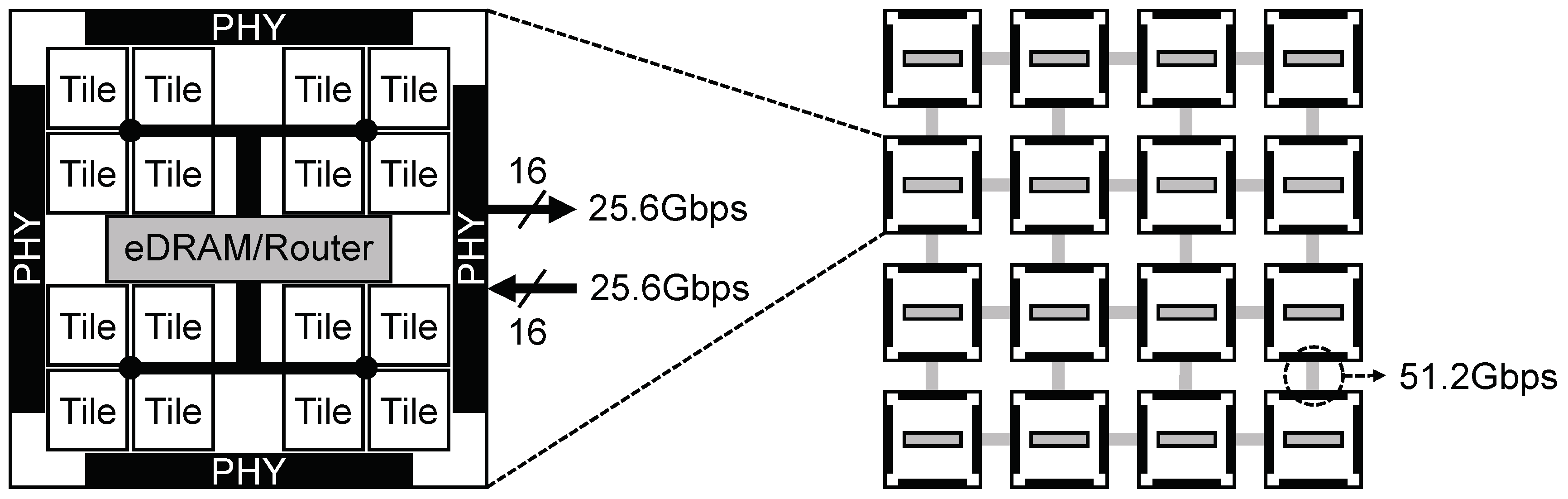
DaDianNao [7] is a custom multi-chip machine-learning architecture proposed to follow trends emphasizing neural networks, such as CNN, characterized by their large size. It achieves much higher performance and energy efficiency compared to existing systems (e.g., GPU) by maximizing parallelism and fully mapping total memory footprints from neurons (nodes in a neural network) and synapses (weights of edges between nodes) to on-chip embedded DRAMs (eDRAM) that require no main-memory access (a major performance/energy bottleneck). Therefore, the number of chips required is determined by the size of the neural network model and input data (e.g., multiple input images forming a batch and concurrently propagating through an image recognition CNN). In Figure 1, we sketched the accelerator chip and its cluster (multi-chip) architecture specified in [7]. A chip has 16 tiles, a central eDRAM (4 MB), fat-tree on-chip interconnect, router fabric, and four physical layers (PHYs) for electrically connecting to other chips. Each tile contains computational logic, a SRAM neuron buffer (16 KB), a local eDRAM (2 MB), and input/output interfaces to the central eDRAM. For PHYs, a commercially available HyperTransport (HT) 2.0 IP block is implemented. Each PHY has bidirectional ports and provides a bandwidth of 25.6 Gbps in each direction with 16 pairs of differential links. The cluster architecture (see the right hand side of Figure 1) is a set of chips arranged in 2D-mesh topology.
2.2. Impact of Off-Chip Interconnect on Performance
We examined the degree of impact of off-chip interconnects on the performance of DaDianNao. The answer differs greatly depending on how neurons and synapses are spread to every chip and which machine-learning phase (inference vs. training) we focus on. To minimize the number of accelerator chips required, we assume that both neurons and synapses of all neural network layers are equally grouped and distributed to every chip. Before the computation for each layer, the authors of [7] assumed that all neurons of the on-going layer, interleaved to every chip, are broadcasted and saved into an extra eDRAM space of each chip. Consequently, a chip exclusively (independently) computes all neurons with its own synapses. Hence, neuron values mainly travel through off-chip interconnects rather than synapses. This method is called model parallelism [10]. However, because latest trends show that synapses are getting light when compared to inflating neurons (as discussed in Section 4.1), we also assume the opposite assumption to reduce inter-chip communication overhead, which is called data parallelism [10]. When using data parallelism, all synapses of an on-going layer before computation for the layer are broadcasted to each chip. A chip independently computes its own neurons with all synapses. In contrast to model parallelism, synapses mainly use off-chip interconnects rather than neurons.
Machine learning has two phases: training (sequential execution of one forward and one backward propagations) and inference (a forward propagation from input data to output result). Conventional CNN accelerators have focused more on the latter; however, the former precedes the latter and also draws keen attention because CNN models evolve rapidly and are applied to more diverse and ever-growing datasets, necessitating continuous training. In this paper, we focus on training rather than inference.
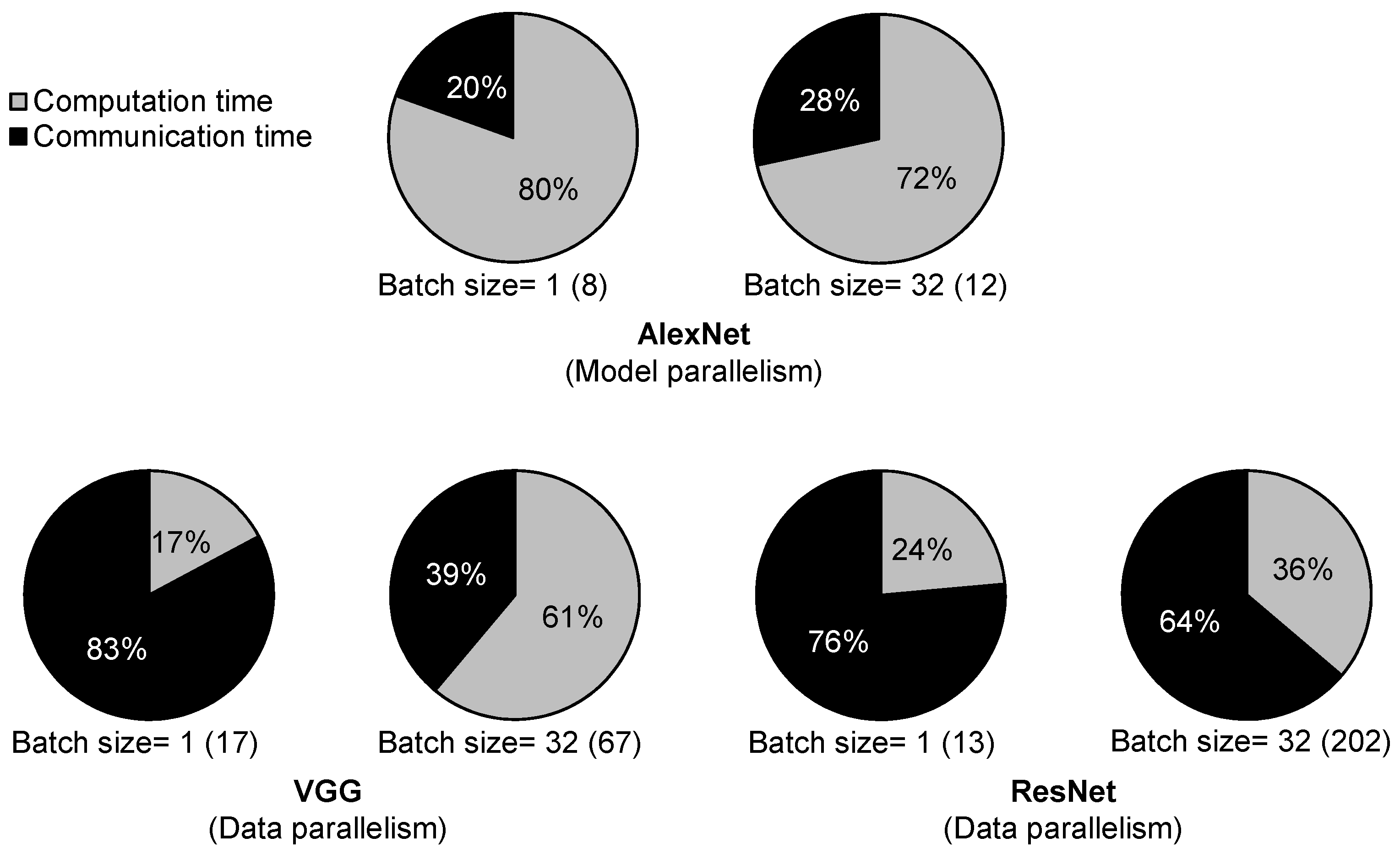
Figure 2 shows the percentages of computation time (including eDRAM access time) and communication time (through off-chip interconnect) in total CNN training time. Our estimation methodology, detailed DaDianNao configuration, and layer information for each CNN are specified in Section 4, Table 1 and Table 2. AlexNet [1], VGG [2], and ResNet [3] were introduced for image recognition in 2012, 2014, and 2015, respectively. The ratios of the number of synapses to that of neurons for more recent CNNs, VGG and ResNet, are lower than that of AlexNet. Therefore, to reduce inter-chip communication, model parallelism is applied for AlexNet whereas data parallelism is applied for VGG and ResNet. The batch size and the number of accelerator chips required (numbers in parentheses) are notated in Figure 2. We do not consider the overlap between computation and communication times because DaDianNao accelerators concurrently start and end (synchronize) their computations for each CNN layer [7] so that the overlap time is small at most. The results show that the communication times of VGG and ResNet are dominant for their total training times. In model parallelism (AlexNet), the neurons increased by a larger batch size (32) enlarge the portion of communication time.
2.3. Current Status of Optical Interconnect Technology
Photonics technology has been dramatically improved in terms of per-fiber bandwidth, fiber cost, optical module chip size, on-package integration, and power consumption. 100 G (gigabit) Ethernet is one of the mainstream for datacenter-scale networks [11] while 400 G Ethernet is expected to be marketed in a few years. Recently, an optical module vendor, MultiPhy, developed a 100 G single-wavelength optical module chip that adapts the PAM-4 (4-level pulse amplitude modulation) technique [11]. While previous 100 G optical interconnect standards are based on the 25 Gbps-per-wavelength capability, enabling 100 Gbps per wavelength is a key technology for developing 400 G optical interconnects without increasing the number of fibers or wavelengths (e.g., 400 G PSM4 or LR4 standards).
Besides datacenter-scale networks, on-chip (on-package) optical interconnects have been actively studied. Off-chip and on-chip optical interconnects are functionally similar. Therefore, their transceiver/receiver modules have the same functional blocks (e.g., laser source, modulator, photodetector, and trans-impedance amplifier). However, on-chip interconnect is more cost-/energy-efficient by using on-chip waveguides (instead of using optical cables and connectors) with a limited connection distance. The silicon optical interposer is critical as it can integrate multiple chips, optical components, and waveguides implemented on the interposer in a single package by 2.5D integration. Recently, several real implementations [12,13] achieved 25–50 Gbps per waveguide on the silicon optical interposer, enabling several Tbps of bandwidth in a package.
3. Optically Interconnected Multi-Chip Machine-Learning System
In the previous section, we discussed the impact of interconnects on DaDianNao performance and the availability of high bandwidth optical interconnects. We show how to implement optical interconnects to a cluster of machine-learning accelerator chips in this section.
3.1. Design Objectives
To fairly demonstrate the potential of optical interconnects for the machine-learning architecture, the design objectives should be aligned to designing a real product. Our implementation is based on the following design objectives:
- Reasonable cost: Although additional cost can be justified by achieving better performance, optical components are still expensive in terms of PHY sizes on silicon and link costs (cable or other forms of waveguides). We keep interconnects from becoming a major factor of the entire system cost.
- Feasibility with current technologies: DaDianNao chip was implemented with a 28 nm process [7]. As discussed in Section 3.2, 100 Gbps of bandwidth can also be achieved by current photonics technology. Our first goal is to apply 100 Gbps interconnects to the current DaDianNao.
- One step forward with the next generation of optical interconnects: In a few years, optical components for 400 G standards will be available. Beyond 100 Gbps, we apply 400 Gbps interconnects to DaDianNao and compare its performance with the existing DaDianNao system.
3.2. Connection to Each Machine-Learning Accelerator
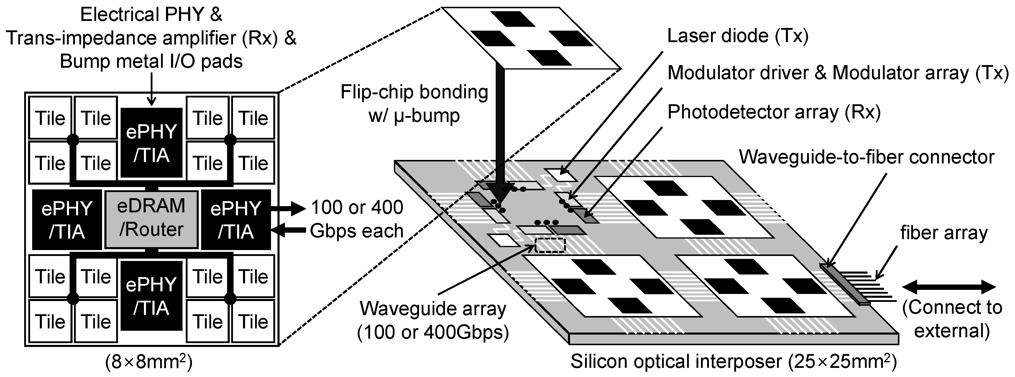
Figure 3 shows a cost-effective and technically feasible design of optical connection to machine-learning accelerators. Obviously, directly interconnecting small DaDianNao chips (about 8 × 8 mm) with optical cables is infeasible and very costly. Therefore, we propose putting several chips into a package by 2.5D integration with a silicon optical interposer and interconnecting multiple packages with off-chip (off-package) interconnects. As shown on the left hand side of Figure 3, we reduced the size of link drivers in an electrical PHY (2.5 mm per PHY, an estimation with reference to [17]) by half to match reduced output loading (reaching only to the silicon interposer) and added a trans-impedance amplifier (a purely electrical component in the optical receiver, Rx) on PHY. We changed I/O pads in PHY to bump metal pads to attach the chip on the silicon interposer through -bumps by flip-chip bonding [13,14] and moved PHYs from the edges toward the center of the chip for stable bonding. The right side of Figure 3 shows the inside of a package including four DaDianNao chips optically connected in 2D-mesh topology. Because the laser diode (in the optical transceiver, Tx), modulator driver (Tx), modulator (Tx), photodetector (Rx), and waveguide can be directly implemented on the silicon interposer [12], we reasonably sized and placed them on a 25 × 25 mm silicon optical interposer with reference to [12]. For example, both we and [12] use a single laser diode for four waveguides and its size is estimated from the photograph of their silicon optical interposer. To mitigate thermal issues, we place the laser diodes outside the area below the accelerator chips. Consequently, two adjacent chips are bidirectionally interconnected. In each direction, a bandwidth of 100 Gbps is provided through four 25 Gbps waveguides or two 50 Gbps waveguides (waveguide pitch can be under 100 um [14]). As we discussed in Section 2.3, a bandwidth of 400 Gbps through four 100 Gbps waveguides (or wavelengths) can also be provided. Outgoing (or incoming) waveguides across the interposer boundary are switched to off-chip (off-package) optical fibers by waveguide-to-fiber connectors [14].
3.3. Network of Multi-Chip Machine-Learning Architecture
We show how to interconnect the multi-chip packages described above for building a cluster. We continue to use the 2D-mesh topology originally adopted in DaDianNao. To exploit the broadcasting characteristic of optical interconnects (e.g., single-write-multi-read), using a serpentine waveguide is an option [18]. However, due to its limited laser source power and large fan-out, it cannot reach beyond the chip boundary.
Figure 4 shows the hardware implementation of the entire multi-chip machine-learning architecture. Six multi-chip packages, for example, can be bonded (or plugged) on the mainboard of a half-height blade server. This is possible because DaDianNao can work without main memory and other storage devices (although the host server requires them). In a blade server, packages are interconnected through fiber bunches (each with eight or four fibers, or fewer fibers with multiple wavelengths while providing 200 or 800 Gbps bidirectionally). Another option is using waveguides implanted on PCB or a flexible ribbon [14]. However, all optical ports of the multi-chip package should be identical (symmetric), and some ports will be connected to another external blade server with fibers and not waveguides. To build a cluster with more than 24 accelerators (chips), multiple blade servers can also be connected through optical fibers. Consequently, fibers are extended out of the server through optic ferrules [14] and up to 64 blade servers (1536 accelerators) can be installed in a standard rack (42U in size).
4. Experimental Methodology
To evaluate the effectiveness of optical interconnects on the performance and energy efficiency of the multi-chip machine-learning system, we modeled DaDianNao multi-chip systems and used famous CNNs for image recognition as well as our arithmetic performance and energy model for measurements.
4.1. Evaluated System and CNN Models
Architectural parameters of DaDianNao accelerator are listed in Table 1. The parameters, except for those of optical interconnect, are the same as the default parameters specified in [7]. The peak performance of the accelerator for training based on 32-bit operations is 2.09 TeraOps/s where four 16-bit multipliers and two 16-bit adders are used for a 32-bit multiplication and a 32-bit addition, respectively. In computing a CNN layer per tile, 8 KB of input neurons and 8 KB of output neurons are saved into a 16 KB SRAM neuron buffer and reused as many times as possible to minimize eDRAM accesses [7]. The peak power per PHY of optical interconnects (100/400 Gbps) includes the power dissipation in the interposer-side optical components. For 100 Gbps PHY (3.5 W), we use the power specification of Intel’s 100 G PSM4 Optical Transceiver [19]. And for 400 Gbps PHY, an optical transceiver module vendor, LUXTERA, estimated the peak power as 6 W [20] and we use its value.
The latency of 100 Gbps optical interconnects between two neighbor accelerators is conservatively assumed to be the same as HT 2.0 latency [7] because a major portion of that latency is not from the components distinguishing electrical interconnect from the optical one, but from the other interconnect layers and the rest of PHY. For one meter of interconnect length, the optical transmission line delay is 2 ns lower than the electrical one [21]. The delay from the modulator driver (Tx) to the trans-impedance amplifier (Rx) in optical PHY (excluding the transmission line delay) does not surpass 1 ns, which is similar to that of functionally equivalent blocks in electrical PHY [22]. By contrast, the latency of 400 Gbps optical interconnects is assumed to be 80 ns longer than the others because the optical interconnects faster than 100 Gbps are generally considered to require Forward Error Correction (FEC) due to a higher Bit Error Rate (BER). The IEEE Standard 802.3 bs [23] has adopted RS (544,514) FEC for the 400 G Ethernet standards using PAM-4, where its latency overhead is estimated as 47 cycles (78 ns at 606 MHz) by [24].
In Table 2, we summarized the structures of the evaluated CNN models. The number X in VGGX, ResNetX, and DenseNetX indicates the total number of convolution layers and fully connected layers composing the respective model. The more recently introduced CNNs have more layers. However, the total synapse size does not always increase correspondingly because the number of synapses per convolution layer is sharply reduced and the number of fully connected layers is decreased, which have many synapses (weights). Accordingly, the ratio of total synapse size to total neuron size was decreased as new CNNs emerged. Therefore, data parallelism is becoming more effective to reduce inter-accelerator communication time compared to model parallelism. In Section 5, except for AlexNet, we only show results using data parallelism as it performs better.
4.2. Arithmetic Performance and Energy Model
We made and used an arithmetic performance and energy model to estimate the total training time and Energy-Delay Product (EDP) of CNN. With only an arithmetic model, we can estimate the computation time of the DaDianNao accelerator and the inter-accelerator communication time on the network for the following reasons:
- The computational unit of DaDianNao has a simple pipeline structure with only three stages and works by in-order execution.
- The clock frequency of the accelerator is constant, so dynamic frequency scaling is not used.
- Every inter-accelerator communication is all-to-all broadcast through a 2D-mesh network so that the execution time can be calculated by a mathematical model [15].
- The throughputs and delays of the computational unit, eDRAM, and interconnect are clearly defined.
Our model consists of three parts: computation, eDRAM, and communication, which are based on Equations (1)–(3), respectively.
In Equation (1), the computation time depends on the operation type causing performance bottleneck. In Equation (2), although eDRAM accesses are pipelined, the access latency should be considered once. Equation (3) from [15] derives all-to-all broadcast time for the 2D-mesh topology. We also considered the pipelined executions between computations and eDRAM accesses. When measuring EDP, we apply the peak power values of DaDianNao chip and its PHY at the proper time interval because all chips and chip-to-chip interconnects are fully utilized and show their maximum throughput during the computation time and communication time, respectively.
5. Evaluation
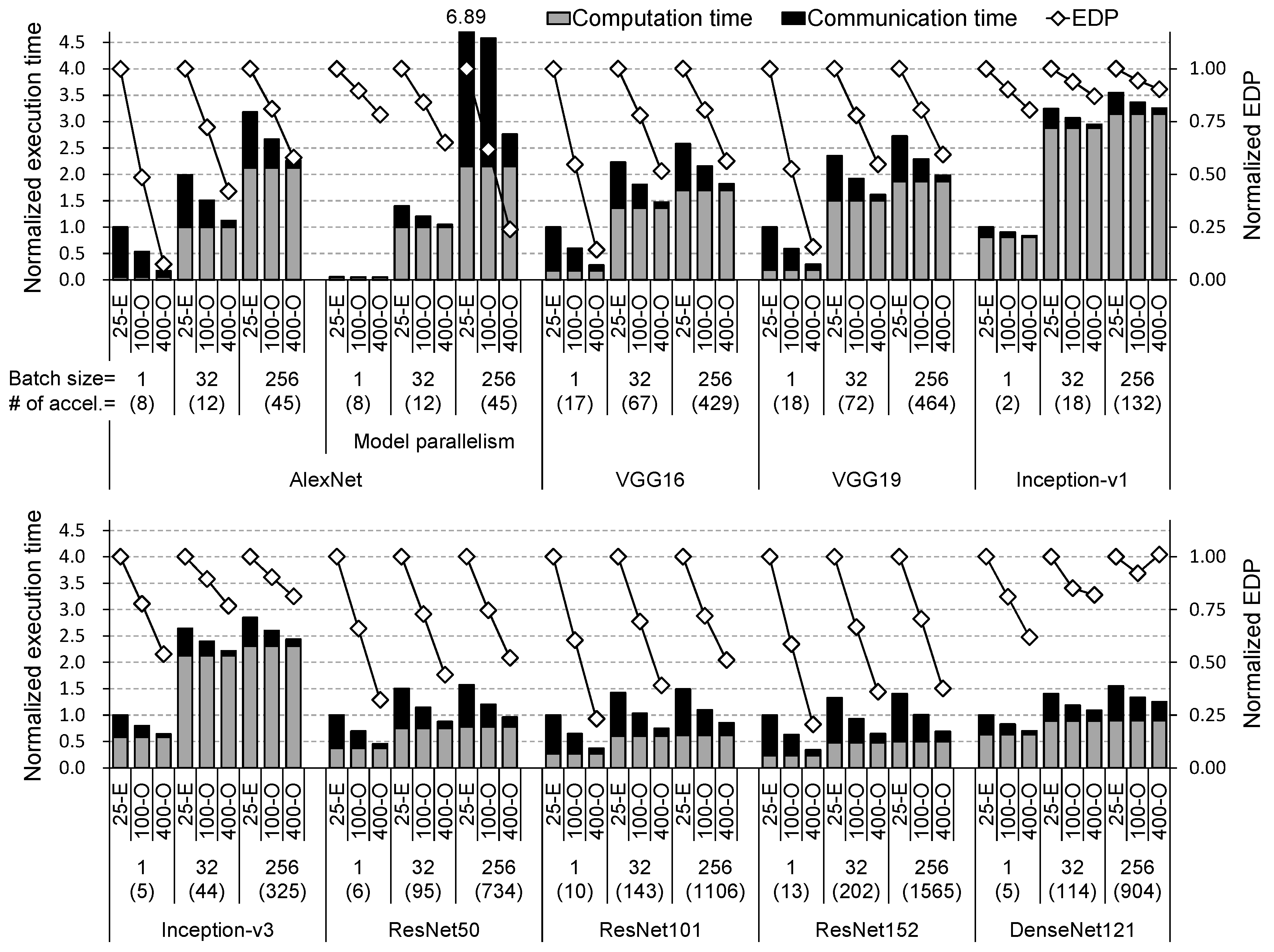
We estimate the training times and energy-efficiency (EDP) of various CNN models on electrically or optically interconnected multi-chip machine-learning architecture. In Figure 5, for nine CNNs, we apply data parallelism by default. For AlexNet only, we add the results by model parallelism. We present the results of three batch sizes: 1, 32, and 256. The number of accelerators (numbers in parentheses) is determined by the total size of neurons and synapses due to limited eDRAM capacity per accelerator. 25-E is the hardware configuration using 25.6 Gbps electrical interconnects (HT 2.0) while 100/400-O is that using 100/400 Gbps optical interconnects. Every execution (training) time is normalized by that of the 25-E case with batch size 1 for each CNN model (for AlexNet, data parallelism is the baseline). Every EDP value is normalized by that of the 25-E case for each batch size and each CNN model. The computation time in Figure 5 includes eDRAM access time. In the following discussion, we assume that, for AlexNet, model parallelism is applied when batch size is 1 or 32 while data parallelism is used for batch size 256 because this is the best choice for performance.
We make the following key observations: First, by applying 100 Gbps and 400 Gbps optical interconnects, execution times are reduced by 20.6% and 35.6% on average, up to 41.1% (VGG19) and 72.2% (VGG16), respectively. Moreover, EDPs (lower is better) are improved by 22.8% and 44.3% on average, up to 47.4% (VGG19) and 85.6% (VGG16), respectively. This clearly shows that the multi-chip machine-learning system can benefit from high bandwidth optical interconnects. Second, when using data parallelism, the portion of computation time in total execution time is increased as the batch size is increased. Therefore, the degree of performance improvement by optical interconnect is decreased because the number of accelerators grows slower when the batch size grows. Thus, each acclerator performs more computation whereas communication time does not noticeably change because synapses are not increased. However, this trend is diminishing as batch size further grows; even with batch size 256, 100 Gbps and 400 Gbps optical interconnects still reduce execution time by an average of 16.9% and 28.4%, respectively. Third, by applying 400 Gbps optical links, EDP of DenseNet121 with batch size 256 gets worse because the communication time reduction is not enough to overcome the energy overhead from optical interconnect. Because the ratio of the total synapse size to the number of accelerators is extremely small, the communication time depends more on node to node latency (see Equation (3)) and does not shrink much due to a longer latency of 400 Gbps optical interconnect. Finally, for CNNs introduced more recently, performance gains from optical interconnect are not diminished. In other words, none of the CNN design trends make optical interconnect unnecessary.
6. Conclusions
In this paper, we have shown the advantages of optical interconnects for multi-chip machine-learning architecture by comparing the performance and energy efficiency of an optically connected multi-chip system with those of an electrically connected one on various CNN models. This work was possible due to the following: (1) We observed that inter-accelerator communication accounts for a significant portion of training time in neural networks. (2) By in-depth consideration of current technologies, a reasonable and practical implementation of optical interconnect was assumed. (3) An arithmetic performance and energy model was made because the network topology and the baseline accelerator have simple structures. We show through evaluation that 100 and 400 Gbps optical interconnects improve the training time (and EDP) by an average of 20.6% (22.8%) and 35.6% (44.3%), respectively, compared to the baseline system with 25.6 Gbps electrical ones for nine CNNs.
Author Contributions
Conceptualization, J.A., Y.R. and E.L.; Data Curation, Y.R.; Formal Analysis, E.L.; Investigation, Y.R.; Methodology, E.L.; Project Administration, J.A.; Resources, Y.R.; Software, E.L.; Supervision, J.A.; Validation, Y.R.; Visualization, Y.R.; Writing—Original Draft, Y.R.; Writing—Review & Editing, J.A.
Funding
This research received no external funding.
Acknowledgments
This research was supported by the Future Semiconductor Device Technology Development Program funded by MOTIE and KSRC (10044735), and Next-Generation Information Computing Development Program through NRF funded by MSIP (2015M3C4A7065647).
Conflicts of Interest
The authors declare no conflict of interest.
References
- Krizhevsky, A.; Sutskever, I.; Hinton, G.E. ImageNet classification with deep convolutional neural networks. In Proceedings of the International Conference on Neural Information Processing Systems (NIPS), Lake Tahoe, NV, USA, 3–6 December 2012; pp. 1097–1105. [Google Scholar]
- Simonyan, K.; Zisserman, A. Very deep convolutional networks for large-scale image recognition. In Proceedings of the International Conference on Learning Representations (ICLR), San Diego, CA, USA, 7–9 May 2015; pp. 1–14. [Google Scholar]
- He, K.; Zhang, X.; Ren, S.; Sun, J. Deep residual learning for image recognition. In Proceedings of the IEEE Conference on Computer Vision and Pattern Recognition (CVPR), Las Vegas, NV, USA, 27–30 June 2016; pp. 770–778. [Google Scholar]
- Szegedy, C.; Liu, W.; Jia, Y.; Sermanet, P.; Reed, S.; Anguelov, D.; Erhan, D.; Vanhoucke, V.; Rabinovich, A. Going deeper with convolutions. In Proceedings of the IEEE Conference on Computer Vision and Pattern Recognition (CVPR), Boston, MA, USA, 7–12 June 2015; pp. 1–9. [Google Scholar]
- Szegedy, C.; Vanhoucke, V.; Ioffe, S.; Shlens, J. Rethinking the inception architecture for computer vision. In Proceedings of the IEEE Conference on Computer Vision and Pattern Recognition (CVPR), Las Vegas, NV, USA, 27–30 June 2016; pp. 2818–2826. [Google Scholar]
- Huang, G.; Liu, Z.; van der Maaten, L. Densely connected convolutional networks. In Proceedings of the IEEE Conference on Computer Vision and Pattern Recognition (CVPR), Honolulu, HI, USA, 21–26 July 2017; pp. 2261–2269. [Google Scholar]
- Chen, Y.; Luo, T.; Liu, S.; Zhang, S.; He, L.; Wang, J.; Li, L.; Chen, T.; Xu, Z.; Sun, N.; et al. DaDianNao: A machine-learning supercomputer. In Proceedings of the Annual IEEE/ACM International Symposium on Microarchitecture (MICRO), Cambridge, UK, 13–17 December 2014; pp. 609–622. [Google Scholar]
- Caulfield, A.M.; Chung, E.S.; Putnam, A.; Angepat, H.; Fowers, J.; Haselman, M.; Heil, S.; Humphrey, M.; Kaur, P.; Kim, J.; et al. A cloud-scale acceleration architecture. In Proceedings of the Annual IEEE/ACM International Symposium on Microarchitecture (MICRO), Boston, MA, USA, 15–19 October 2016. [Google Scholar]
- Park, J.; Sharma, H.; Mahajan, D.; Kim, J.K.; Olds, P.; Esmaeilzadeh, H. Scale-out acceleration for machine learning. In Proceedings of the Annual IEEE/ACM International Symposium on Microarchitecture (MICRO), Cambridge, MA, USA, 14–18 October 2017; pp. 367–381. [Google Scholar]
- Dean, J.; Corrado, G.S.; Monga, R.; Chen, K.; Devin, M.; Le, Q.V.; Mao, M.Z.; Ranzato, M.A.; Senior, A.; Tucker, P.; et al. Large scale distributed deep networks. In Proceedings of the International Conference on Neural Information Processing Systems (NIPS), Lake Tahoe, NV, USA, 3–8 December 2012; pp. 1223–1231. [Google Scholar]
- EENews EUROPE. Single-Wavelength PAM4 DSP Chip Delivers 100 G. Available online: http://www.eenewseurope.com/news/single-wavelength-pam4-dsp-chip-delivers-100g (accessed on 25 May 2018).
- Okamoto, D.; Urino, Y.; Akagawa, T.; Akiyama, S.; Baba, T.; Usuki, T.; Miura, M.; Fujikata, J.; Shimizu, T.; Okano, M.; et al. Demonstration of 25-Gbps optical data links on silicon optical interposer using FPGA transceiver. In Proceedings of the European Conference on Optical Communications (ECOC), Cannes, France, 21–25 September 2014. [Google Scholar]
- Kim, D.; Au, K.Y.; Li, H.Y.; Luo, X.; Ye, Y.L.; Bhattacharya, S.; Lo, G.Q. 2.5D Silicon optical interposer for 400 Gbps electronic-photonic integrated circuit platform packaging. In Proceedings of the Electronics Packaging Technology Conference (EPTC), Singapore, 6–9 December 2017. [Google Scholar]
- Patterson, D.; Sousa, I.D.; Achard, L.M. The future of packaging with silicon photonics. Chip Scale Rev. 2018, 21, 14–25. [Google Scholar]
- Sun, C.; Wade, M.T.; Lee, Y.; Orcutt, J.S.; Alloatti, L.; Georgas, M.S.; Waterman, A.S.; Shainline, J.M.; Avizienis, R.R.; Lin, S.; et al. Single-chip microprocessor that communicates directly using light. Nature 2015, 528, 534–538. [Google Scholar] [CrossRef] [PubMed] [Green Version]
- Gonzalez, R.; Horowitz, M. Energy Dissipation in General Purpose Microprocessors. IEEE J. Solid-State Circuits 1996, 31, 1277–1284. [Google Scholar] [CrossRef]
- Mansuri, M.; Jaussi, J.E.; Kennedy, J.T.; Hsueh, T.; Shekhar, S.; Balamurugan, G.; O’Mahony, F.; Roberts, C.; Mooney, R.; Casper, B. A Scalable 0.128-to-1Tb/s 0.8-to-2.6pJ/b 64-lane Parallel I/O in 32nm CMOS. In Proceedings of the International Solid-State Circuits Conference Digest of Technical Papers (ISSCC), San Francisco, CA, USA, 17–21 February 2013; pp. 402–403. [Google Scholar]
- Vantrease, D.; Schreiber, R.; Monchiero, M.; McLaren, M.; Jouppi, N.P.; Fiorentino, M.; Davis, A.; Binkert, N.; Beausoleil, R.G.; Ahn, J. Corona: System Implications of Emerging Nanophotonic Technology. In Proceedings of the International Symposium on Computer Architecture (ISCA), Beijing, China, 21–25 June 2008; pp. 153–164. [Google Scholar]
- Intel. 100G Parallel Single Mode Data Center Connectivity. Available online: https://www.intel.com/content/dam/www/public/us/en/documents/product-briefs/optical-transceiver-100g-psm4-qsfp28-brief.pdf (accessed on 23 June 2018).
- Welch, B. 400G Optics—Technologies, Timing, and Transceivers. In Proceedings of the IEEE P802.3bs 200 GbE & 400 GbE Task Force Interim Meeting, Norfolk, VA, USA, 12–14 May 2014. [Google Scholar]
- Wang, Z.; Xu, J.; Yang, P.; Wang, X.; Wang, Z.; Duong, L.H.K.; Wang, Z.; Maeda, R.K.V.; Li, H. Improve chip pin performance using optical interconnects. IEEE Trans. VLSI Syst. 2016, 24, 1574–1587. [Google Scholar] [CrossRef]
- Chen, G.; Chen, H.; Haurylau, M.; Nelson, N.A.; Albonesi, D.H.; Fauchet, P.M.; Friedman, E.G. On-chip copper-based vs. optical interconnects: delay uncertainty, latency, power, and bandwidth density comparative predictions. In Proceedings of the International Interconnect Technology Conference (IITC), Burlingame, CA, USA, 5–7 June 2006; pp. 39–41. [Google Scholar]
- IEEE LAN/MAN Standards Committee. IEEE Std 802.3bs-2017 (IEEE Standard for Ethernet). Available online: http://www.ieee802.org/3/bs/ (accessed on 25 May 2018).
- Wang, X.; Wang, T.; Yang, W. Proposal for 400 GbE FEC Architecture. In Proceedings of the IEEE P802.3bs 200 GbE & 400 GbE Task Force Plenary Meeting, Berlin, Germany, 9 March 2015. [Google Scholar]
Figure 1.
DaDianNao chip and cluster (multi-chip) architecture.

Figure 2.
The ratios of computation and communication time in total training time of various CNNs. A number in parentheses represents the number of accelerator chips required.
Figure 2.
The ratios of computation and communication time in total training time of various CNNs. A number in parentheses represents the number of accelerator chips required.

Figure 3.
Modified DaDianNao chip and its optically connected multi-chip package.

Figure 4.
A 2D-mesh topology implementation using blade servers (each with multi-chip packages) and a rack-scale machine-learning system implementation.
Figure 4.
A 2D-mesh topology implementation using blade servers (each with multi-chip packages) and a rack-scale machine-learning system implementation.

Figure 5.
The training times (computation/eDRAM + communication) and EDP of nine CNNs on electrically/optically connected multi-chip machine-learning architectures. Data parallelism is applied by default. 25-E is the system using 25.6 Gbps electrical links and 100/400-O is that using 100/400 Gbps optical ones. The execution time is normalized by that of 25-E with batch size 1 for each CNN. EDP is normalized by that of 25-E for each batch size.

Table 1.
Parameters of the DaDianNao accelerator chip.
| Parameter | Value | Parameter | Value |
|---|---|---|---|
| Frequency | 606 MHz | Local eDRAM latency | 3 cycles |
| # of tiles | 16 | Central eDRAM latency | 10 cycles |
| # of 16-bit multipliers | 288/tile | SRAM buffer capacity | 16 KB/tile |
| # of 16-bit adders | 288/tile | Local eDRAM capacity | 2 MB/tile |
| Peak performance | 2.09 TeraOPS | Central eDRAM capacity | 4 MB |
| Peak power w/o PHY | 7.96 W | Peak per-PHY power | |
| - Electrical 25.6 Gbps | 2.00 W | ||
| - Optical 100 Gbps | 3.50 W | ||
| - Optical 400 Gbps | 6.00 W | ||
| Accel.-to-accel. bandwidth | (bidirectional) | Accel.-to-accel. latency | |
| - Electrical 25.6 Gbps | 6.4 GB/s | - Electrical 25.6 Gbps | 80 ns |
| - Optical 100 Gbps | 25 GB/s | - Optical 100 Gbps | 80 ns |
| - Optical 400 Gbps | 100 GB/s | - Optical 400 Gbps | 160 ns |
Table 2.
Summary of the evaluated CNN models.
| Parameter | AlexNet | VGG | VGG | Inception | Inception | ResNet | ResNet | ResNet | DenseNet |
|---|---|---|---|---|---|---|---|---|---|
| [1] | 16 [2] | 19 [2] | - v1 [4] | -v3 [5] | 50 [3] | 101 [3] | 152 [3] | 121 [6] | |
| Year introduced | 2012 | 2014 | 2014 | 2015 | 2015 | 2015 | 2015 | 2015 | 2016 |
| # of layers | 14 | 22 | 25 | 73 | 111 | 125 | 244 | 363 | 306 |
| (convolution/fully connected) | (5/3) | (13/3) | (16/3) | (20/1) | (56/1) | (49/1) | (100/1) | (151/1) | (120/1) |
| Total synapse [MB] | 233 | 528 | 548 | 27 | 105 | 97 | 170 | 229 | 30 |
| Total neuron * [MB] | 172 | 1860 | 2019 | 587 | 1446 | 3290 | 4956 | 7014 | 4061 |
| Ratio in size (synapse/neuron) | 1.35 | 0.28 | 0.27 | 0.05 | 0.07 | 0.03 | 0.03 | 0.03 | 0.01 |
* Input image size and batch size are assumed as 224 × 224 × 3 and 32, repectively.
© 2018 by the authors. Licensee MDPI, Basel, Switzerland. This article is an open access article distributed under the terms and conditions of the Creative Commons Attribution (CC BY) license (http://creativecommons.org/licenses/by/4.0/).
Share and Cite
MDPI and ACS Style
Ro, Y.; Lee, E.; Ahn, J.H. Evaluating the Impact of Optical Interconnects on a Multi-Chip Machine-Learning Architecture. Electronics 2018, 7, 130. https://doi.org/10.3390/electronics7080130
AMA Style
Ro Y, Lee E, Ahn JH. Evaluating the Impact of Optical Interconnects on a Multi-Chip Machine-Learning Architecture. Electronics. 2018; 7(8):130. https://doi.org/10.3390/electronics7080130
Chicago/Turabian StyleRo, Yuhwan, Eojin Lee, and Jung Ho Ahn. 2018. "Evaluating the Impact of Optical Interconnects on a Multi-Chip Machine-Learning Architecture" Electronics 7, no. 8: 130. https://doi.org/10.3390/electronics7080130
Note that from the first issue of 2016, this journal uses article numbers instead of page numbers. See further details here.