Article

A Bandwidth-Enhanced Differential LC-Voltage Controlled Oscillator (LC-VCO) and Superharmonic Coupled Quadrature VCO for K-Band Applications

1
Beijing Key Laboratory of Radio Frequency IC Technology for Next Generation Communications, Institute of Microelectronics, Chinese Academy of Sciences, Beijing 100029, China
2
Institute of Microelectronics, University of Chinese Academy of Sciences, 19A Yuquan Rd., Shijingshan District, Beijing 100049, China
3
COMSATS University, Wah Campus, G. T. Road, Wah Cantt 47040, Pakistan
*
Author to whom correspondence should be addressed.
Electronics 2018, 7(8), 127; https://doi.org/10.3390/electronics7080127
Submission received: 29 June 2018 / Revised: 17 July 2018 / Accepted: 20 July 2018 / Published: 25 July 2018

Abstract

:
A novel varactor circuit exhibiting a wider tuning range and a new technique for quadrature coupling of LC-Voltage Controlled Oscillator (LC-VCO) is presented and validated on a 25 GHz oscillator. The proposed varactor circuit employs distribute-biased parallel varactors with a series inductor connected at both ends of the varactor bank to extend the tuning range of the oscillator. Similarly, the quadrature coupling is accomplished by employing the 2nd harmonic, explicitly generated in the stand-alone free-running differential oscillator using frequency doubler. As an example, the Differential VCO (DVCO) is tunable between 20 GHz and 31 GHz and exhibits the best Phase Noise ( P N ) of −100 dBc/Hz at 1 MHz offset frequency. Similarly, the Quadrature VCO (QVCO) covers 42% tuning bandwidth around 25 GHz oscillation frequency, which is significantly wider than other state-of-the-art VCOs at comparable frequencies. In addition, all the oscillators are designed in class-C to further improve their performances both in term of low power and low phase noise. The presented oscillators are designed using high-performance SiGe HBTs of the GlobalFoundries (GFs) 130 nm SiGe BiCMOS 8HP process. The presented DVCO and QVCO draw currents of approximately 10 mA and 21 mA, respectively from a 1.2 V supply.

1. Introduction

Modern wireless communication is transforming into future 5G and the demand for high data-rate communication with increased bandwidth requirements is increasing. Voltage Controlled Oscillator (VCO) as one of the key components is used in modern phase-locked loop (PLL) to provide local frequency signal. It is critical for VCOs that can robustly provide wider tuning range ( T R ) at mm-wave frequency region with low phase noise. To date, many oscillators featuring low-power consumption ( P D C ) , low phase noise ( P N ) and wide T R in K -band have been reported [1,2,3,4,5,6,7,8]. However, it is still challenging and uncommon to design VCO with optimized trade-off to simultaneously achieve a wide T R with low P N and low P D C . For example, in [1], two K -band S i G e bipolar VCOs using transformer-coupled varactors are presented. But they can only be tuned from 18.6 to 21.2 GHz and 20.4 GHz to 24.2 GHz, resulting only in 13 % and 17 % tuning ranges, respectively. Similarly, triple-couple inductor as part of the L C -Tank, to couple multiple varactors, is implemented to get more linear and wider T R , but only 15.8 % T R is achieved at K -band [2]. In [3], the reported differential VCO utilizes current-reuse and transformer-feedback techniques fabricated in the standard bulk 90 nm CMOS process, can only achieve 4.8 % tuning bandwidth at K -frequency band. Similarly, various Negative Capacitance ( N C ) circuits were integrated with traditional LC-VCOs to cancel out the parasitics (produced mainly by the L C -tank and cross-coupled pair) to expand the T R [9,10]. For example, in [9], the N C circuit is used to shift the oscillation frequency from 20.1 to 31.6 GHz, which, although it improves the T R % from 5.7 to 12.4 % , it makes the power consumption too high (590 mW) and worsens the phase noise to −88 dBc/Hz. Similarly, a tunable differential N C circuit was designed in [10] to compensate the parasitic capacitances and is realized by connecting the N C circuit to the source of the cross-coupled transistors of the LC-VCO; however, it affected the start-up condition. Therefore, the N C of [10] only had a small effect on the resonance frequency ( f R E S ) and T R .
Similarly, the Quadrature Voltage Controlled Oscillators (QVCOs) play an important role in many fully-integrated, low cost, radio-frequency transceivers requiring I / Q modulation/demodulation. To provide Quadrature Local Oscillator ( L O ) signals, various techniques are endorsed. Two approaches are very common for quadrature L O generation: (1) divide-by-two [11] and (2) polyphase filter techniques [12]. However, the earlier is more power hungry since the system oscillator needs to be operated at twice the desired frequency, while the later suffers from low quadrature accuracy as well as requiring an additional buffer to boost the output power. Later, the L C -based QVCOs are presented for the generation of quadrature L O signals without employing divide-by-two or polyphase filters, which resulted in huge reductions in power consumption as well as improved accuracy [13].
L C -based QVCOs are obtained by employing antiphase coupling between two identical differential oscillators. The antiphase connection is realized using a coupling network, either an active or passive coupling. The circuit techniques employing active coupling are parallel coupling (P-QVCO) [13], series coupling (S-QVCO) [3], top- and bottom-series coupling (TS-QVCO and BS-QVCO) [14], sub- and super-harmonic coupling [15,16], body-biased coupling [17], In-phase injection-coupling [18], complementary coupling [19] etc. Similarly, passive coupling techniques like inductor-based superharmonic coupling [20], transformer coupling [21], and coupling using transmission lines [22] are used for quadrature L O generation.
Firstly, we emphasized to attain wider T R at K -frequency band. To realize this, we proposed a novel varactor circuit that consists of two similar branches of varactors, biased at different voltages. They are also cascaded with two inductors, each connected to the common nodes of the varactor bank at both sides. The proposed varactor scheme exhibits wider T R at mm-wave frequency. Besides, the T R of the VCO is enhanced by properly designing the VCO-core and aligning the consecutive frequency tuning characteristics with sufficient overlap margin to avoid blind zones between them. In addition, a novel technique for quadrature generation is proposed in this work. Subsequently, the two similar bandwidth-enhanced differential oscillators that we proposed in our first work are locked in quadrature by implementing the proposed quadrature generation technique. Hence, both the differential and quadrature VCOs cover a minimum of 42% bandwidth around 25 GHz with total power consumptions of 12 mW and 25 mW, respectively from 1.2 V supply.
The rest of the paper is organized as follows. The technical arguments for the selection of an appropriate fabricating technology as well as the L C -oscillator topology based on their inherent P N and power consumption characteristics are outlined in Section 2. Section 3 describes the T R and design implementation of the proposed varactor circuit. Section 4 reports the post-layout simulation results of the differential and quadrature oscillators, both integrated with proposed wideband varactor circuit. The entire work is finally concluded in Section 5.

2. Design Consideration for Low PN and Wideband VCO

2.1. Technology Overview

Moving up with frequency, the losses increase intensively and requirements of the communication systems become more and more rigorous. So, the devices must have higher f t and higher power handling capabilities in order to meet the stringent requirements of the communication systems. State-of-the-art SiGe BiCMOS technology can stand as the best candidate for its excellent performance, featuring high ft/fmax, high reliability and extended temperature range, making this technology a potential candidate for mm-wave circuit designs.
The VCO, as part of the frequency synthesizer, is a key building block in high performance wireless and wireline communication systems. Previously, integrated mm-wave VCOs have been designed using either GaAs or other III-IV technologies [23,24]. But there has always been an interest to develop S i -based mm-wave VCOs due to its lower fabrication cost and that it can be easily scaled compared to III–IV technologies [25,26]. In addition to the implementation cost and system integration, the SiGe BiCMOS provides the degree of freedom by using MOSFET and HBTs in the same integrated circuits making this technology very appropriate for designing high-performance R F circuits with digital logics on the same substrate. Moreover, SiGe HBTs provide high gain and improved noise performance at extremely low current densities. Also, with lower 1 / f noise, four times better transconductance and higher breakdown voltage (for the same fmax), the BiCMOS technology stands as an appropriate technology for the design of high performance VCOs and power amplifiers etc. The proposed wide T R mm-wave VCO has been designed using 130 nm SiGe BiCMOS technology and is intended to be integrated in a complete frequency synthesizer for K -band applications.

2.2. Class-C

Among several VCO topologies, L C -VCO topology with core transistors operating in Class-B and Class-C are implemented for low P N and wide T R . However, for the same power consumption, 3.9 dB improvement on P N is expected when compared to Class-B [27]. Depicted in Figure 1a, is a typical arrangement of Class-C oscillator in which the base of one transistor in the cross-coupled pair is ac-coupled from the drain of the other, using C b i a s . In addition, a common dc-bias is applied at the bases of cross-coupled transistors. With this arrangement, the average maximum voltage on the cross-coupled pair can be observed much smaller in Class-C than in Class-B, thereby preventing the core transistors to enter into the saturation region, hence results in better phase noise. However, depending on whether or not the large tail capacitance C t a i l is connected to the common node of transistors Q 1 and Q 2 , the oscillator is operated fully in Class-C or Class-B [27]. A detailed comparative study of class-B and class-C oscillators has been carried-out in [28].
Another oscillator topology that can be widely used for high-frequency applications and particularly in the application of bipolar oscillators, is the Colpitts oscillator (see Figure 1b). A comprehensive analysis of phase noise in bipolar Colpitts oscillator as well as its comparison with Class-B oscillator is conducted in [29]. This comparative study is carried out by assuming the oscillator to operate in current-limited regime for a given tank impedance and bias current. However, when the analysis is extended to maximize the oscillation amplitude, a better phase noise is achieved. Nevertheless, the Colpitts oscillator can also be allowed to decrease its phase noise by setting the feedback factor “n” (from tank to the BJT emitter) high; but this would result in large power consumption and less efficiency [30]. Hence, it can be concluded that among the aforementioned topologies we discussed, Class-C L C -Oscillator is a superior topology over others in terms of low power and low P N for a given tank impedance, supply voltage and oscillation frequency, which has been chosen for our design.
Low P N is another significant measure of the oscillator. Single-sideband Phase noise ( L ) of a generic harmonic oscillator at an offset frequency ( Δ ω ) from the carrier can be expressed as (1) [31].
L ( Δ ω ) = ( ω 0 Δ ω ) 2 [ k B T R S V 0 2 ( 1 + F ) ]
where k B and T are the Boltzmann constant and temperature, respectively. R S , V 0 , F and ω 0 denote the inductor’s parasitic series resistance, oscillation amplitude, noise factor and oscillation frequency, respectively. It can be stated by looking at (1) that the phase noise decreases as the dissipated power “ P D C ” is increased at an offset frequency Δ ω . Moreover, an oscillator topology, yielding low noise factor “ F ” and providing a high amplitude oscillation “ V 0 ” will further help to reduce the phase noise.

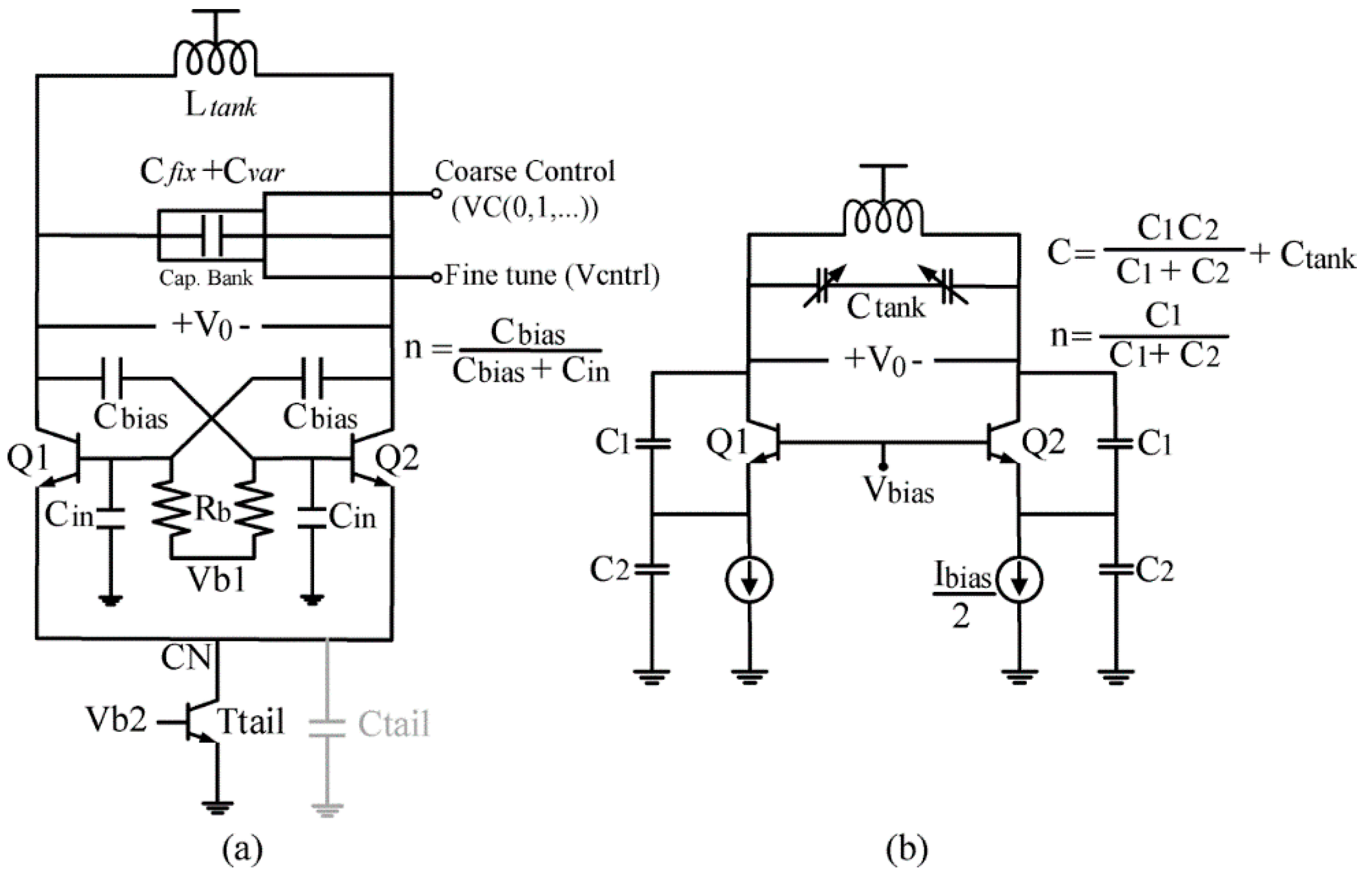
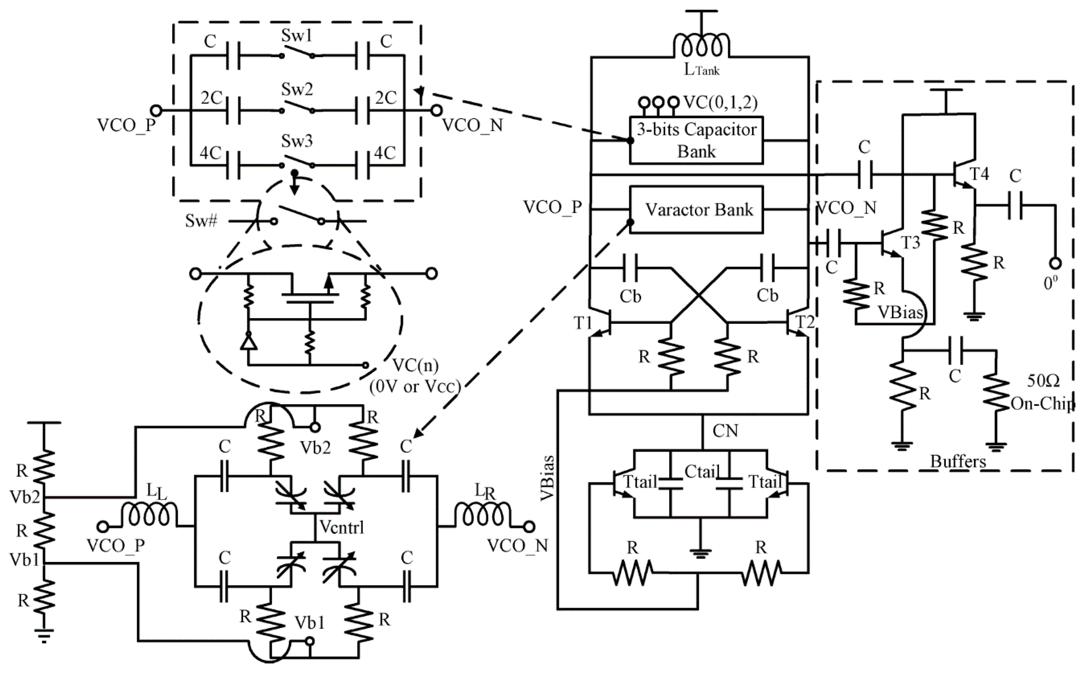
3. Circuit Description
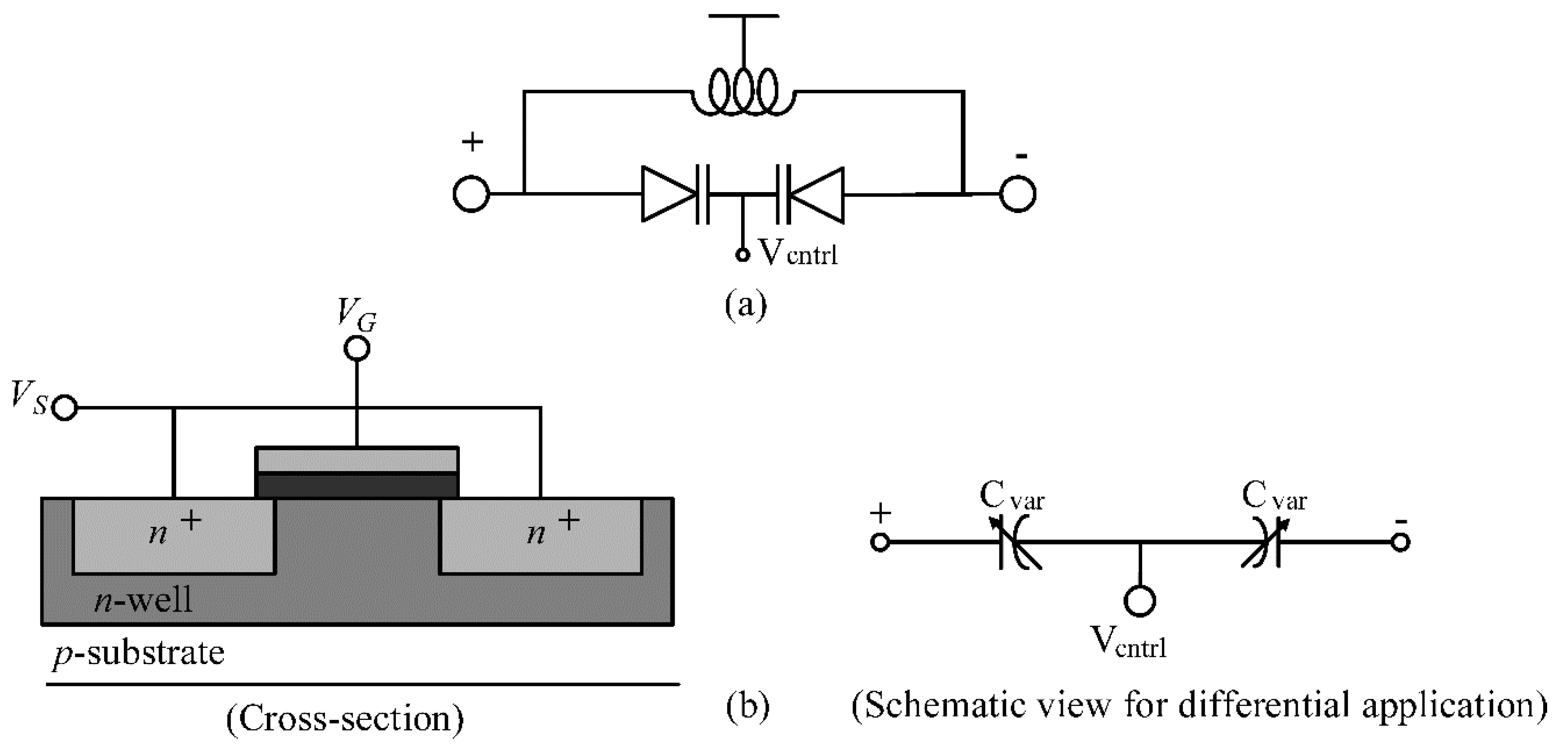
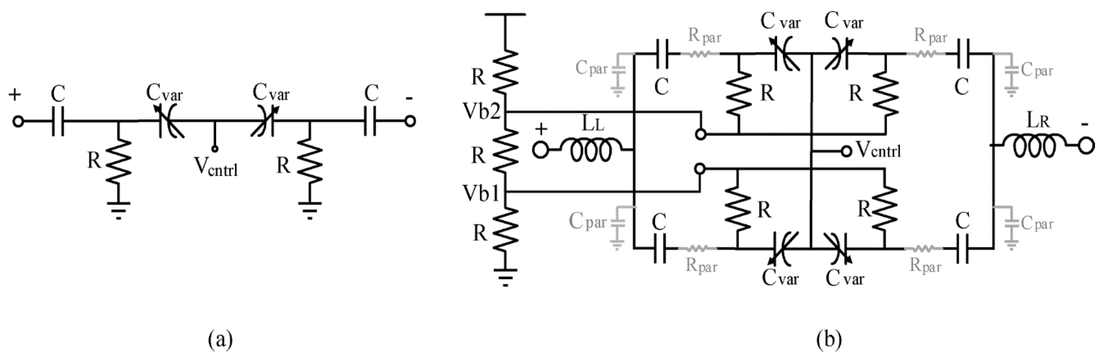
The traditional Class-C oscillator arrangement depicted in Figure 1a, consists of a dc-biased cross-coupled transistors pair, a varactor, fix capacitor bank and an inductor. If the differential transconductance produced by the cross-coupled transistors compensates the tank losses, then the frequency of oscillation will be given by (2).
f R E S = 1 2 π L t a n k ( C V a r + C f i x )
where C V a r and C f i x represent the capacitances of the varactor and switched-capacitor bank, respectively, that are responsible to coarsely control and finely tune the oscillation frequency. The coarse control of the oscillation frequency can be accomplished using the input control voltage correspond to VC (0, 1, …), while the fine tuning of the oscillation frequency can be done using V c n t r l .

3.1. Varactor

Varactor is employed to tune the oscillation frequency of the oscillator by changing the control voltage across it. For a varactor, the two parameters are very important: (a) the capacitance range i.e., the ratio of the maximum and minimum capacitances that the varactor can provide as the applied voltage is varied, and (b) the quality factor, which is limited by the series resistance within the varactor structure [32]. These two parameters exhibit a trade-off as the frequency goes high, i.e., when the capacitance is increased, the quality factor is decreased. To employ a high Q varactor, the channel length must be minimized. However, for a minimum channel length, the overlap capacitance between the gate and source/drain terminals becomes relatively large, hence limiting the T R . On the other hand, to get the wider T R , the size of the varactor is increased. However, it is not feasible at high frequencies e.g., at 25 GHz, since the contribution of the capacitive part of the tank is more significant in K -band. Particularly, the varactor quality factor degrades intensively if the size of the varactor is set too high, which may dominate the resonator loss and hence dissatisfy the startup oscillation condition. In order to re-start the oscillation, one may increase the core transistors size, but again, the size of the core transistors cannot be set too large due to the parasitics they add to the tank, which would, in turn, increase the C f i x , degrading the T R and tensing the already limited capacitance budget. In summary, it is difficult to achieve high Q and wide T R simultaneously.
Previously, the two types of varactors named as p-n junction diode and n-type accumulation mode-MOS A-MOS varactors are employed for the implementation of wideband VCOs. The p-n diode fundamentally works in reverse bias and it needs to be properly biased with the tank to avoid the forward biasing. One possible formation is shown in Figure 2a, called direct-coupling. However, the critical limitation of this structure is that V c n t r l always needs to be higher than the supply voltage to limit the forward biasing. Otherwise, the junction will turn-on and the quality factor will drop significantly. Another type of varactor that is mostly adopted to tune the oscillation frequency is the nMOS varactor. The BiCMOS 8HP process provides a standard thin oxide nMOS varactor for differential circuits. Presented in Figure 2b (left) is the cross-section view and its corresponding differential version of the varactor that can be employed as a variable capacitor. The variable capacitance is achieved as the device is biased from depletion to accumulation [33,34].
Regardless the type of varactor used in the oscillator, their conventional structure always suffers from the limited T R .

3.2. Proposed Varactor Circuit Implementation

It is aimed to attain the widest possible T R around 25 GHz oscillation frequency. To realize a wideband VCO, a wideband varactor circuit shown in Figure 3b is proposed exhibiting an extended T R . Unlike the conventional design shown in Figure 3a, the proposed design consists of two similar branches of varactors connected in parallel. Each varactor pair is R C -biased at a different bias voltage generated through the resistive divider circuit. Equal step of biasing voltage is chosen from 1.2 V supply. Hence V b 1 and V b 2 are chosen as 0.4 V and 0.8 V, respectively. Thus, the steep part of each characteristic curve in the entire T R is centered on its corresponding biasing voltage, thereby presenting a more stretched capacitance over the entire voltage control range. In addition, two inductors each at both ends (in series to the varactor bank) are added to extend the T R . The series connection of inductors improves the C _ m a x / C _ m i n ratio of the varactor bank and also cancels the parasitic capacitances introduced by the parallel varactor branches leading to achieve even more wider T R . The varactor’s series inductors ( L L & L R ) in Figure 3b have significant effects on the VCO’s operating frequency as well as the tuning range, since they are in parallel to the tank inductor ( L T a n k ). The T R can be increased or decreased by respectively increasing or decreasing the value of series inductors. However, a very large value inductor may dissatisfy the startup of the oscillator as well as the desired center frequency able to go lower. Likewise, a very small value inductors exhibit small capacitance and thus presenting narrower tuning range. Therefore, the series inductors need to be decided based on the desired center frequency as well as the required tuning range. In our designed oscillators, 136 pH inductors are selected to optimize the oscillator center frequency around 25 GHz with tuning range from 20 GHz to 31 GHz.
Comparison of the same and single frequency tuning characteristic, based on proposed and traditional varactor circuits, is presented in Figure 4. The proposed tuning circuit when incorporated in class-C LC-VCO (see Figure 7) resulted in an overall wider T R .
The simulation result of Figure 4 is performed by first implementing the conventional varactor circuit with two identical branches in parallel with a common biasing voltage. Then, the same number of varactor branches as in conventional design, are implemented in the proposed varactor circuit so that the overall capacitance in both cases are maintained. By implementing the proposed varactor circuit, the covered frequency range is considerably extended more than the range covered with the traditional varactor circuit. The range covered based on typical and proposed varactors are 1.51 GHz and 2.37 GHz respectively, which is 56% more wider than the baseline T R . These analyses are based on when the input control word to the capacitor bank is 101 which corresponds to VC0, VC1, VC2, respectively. Of course, it will accordingly change as we choose the bottom and top tuning characteristics in the whole T R .
Plots in Figure 5 represent the F(V) curves of the same discrete tuning curve with different biasing voltage combinations applied to the varactors. Based on the most widely covered tuning bandwidth, we chose the varactor biasing voltage as 0.4 V and 0.8 V as Vb1 and Vb2, respectively.
Next, the performance of both the oscillators will be discussed. All simulation results presented in the following section are done with post-layout.

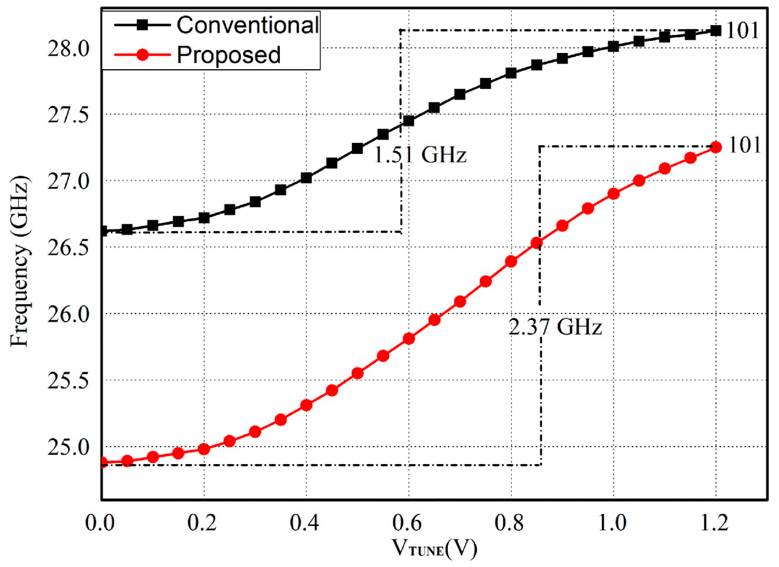
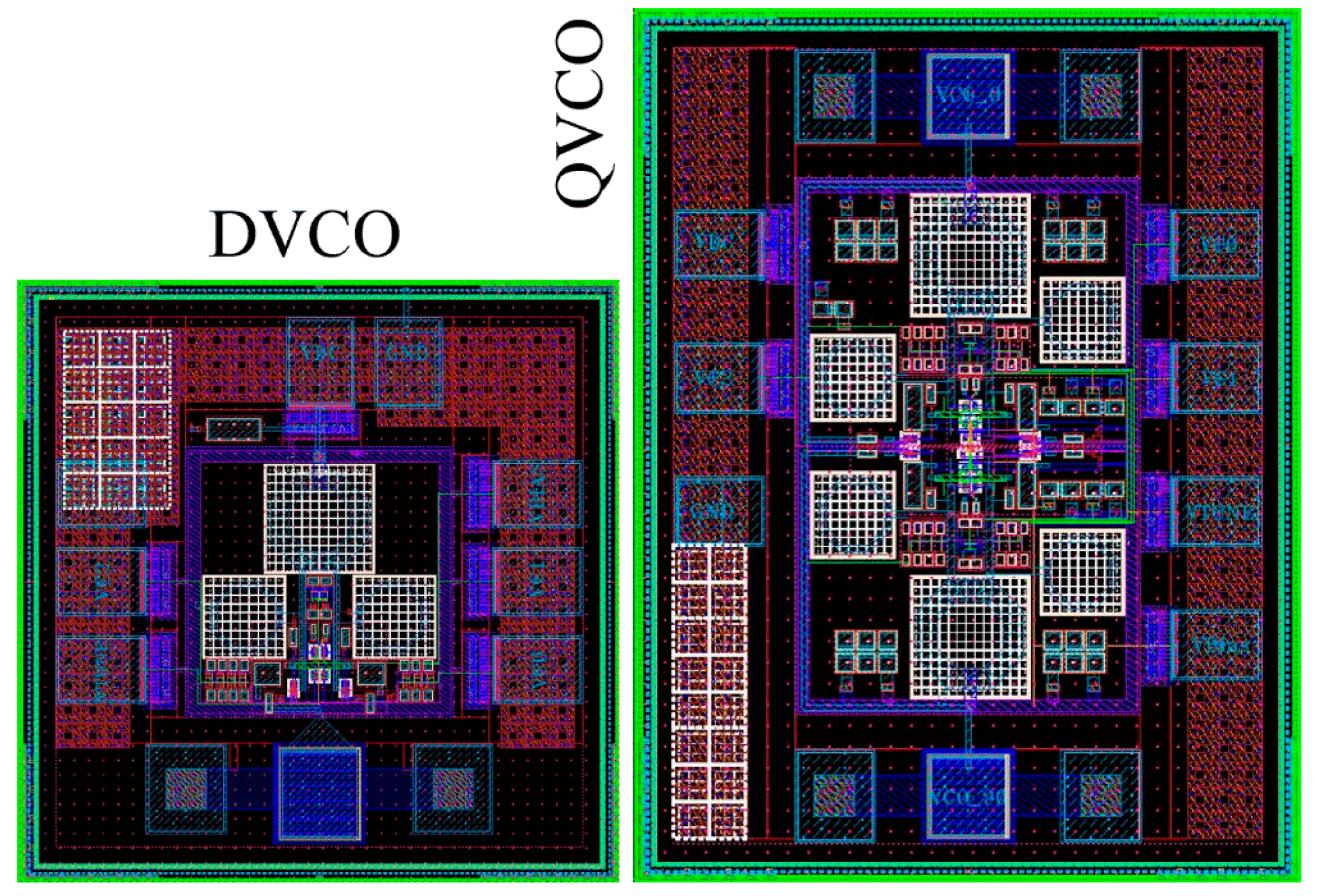
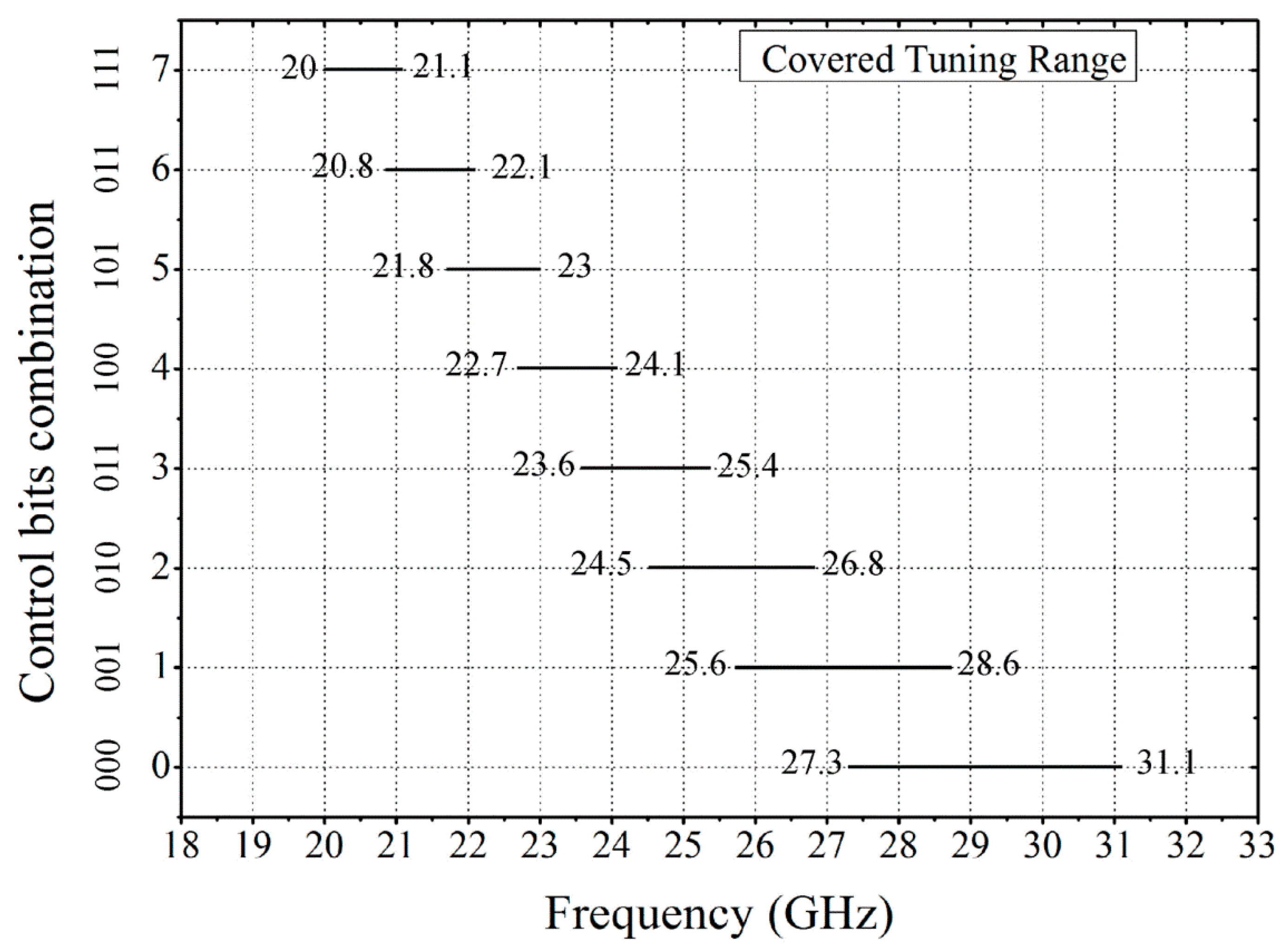
4. Post-Layout Simulation Results and Discussion

The designed prototype of differential and quadrature VCOs are presented in Figure 6, with total covered area (including bond pads) of 0.45 mm2 and 0.7 mm2, respectively. Their corresponding schematic circuits are provided in Figure 7 and Figure 9.

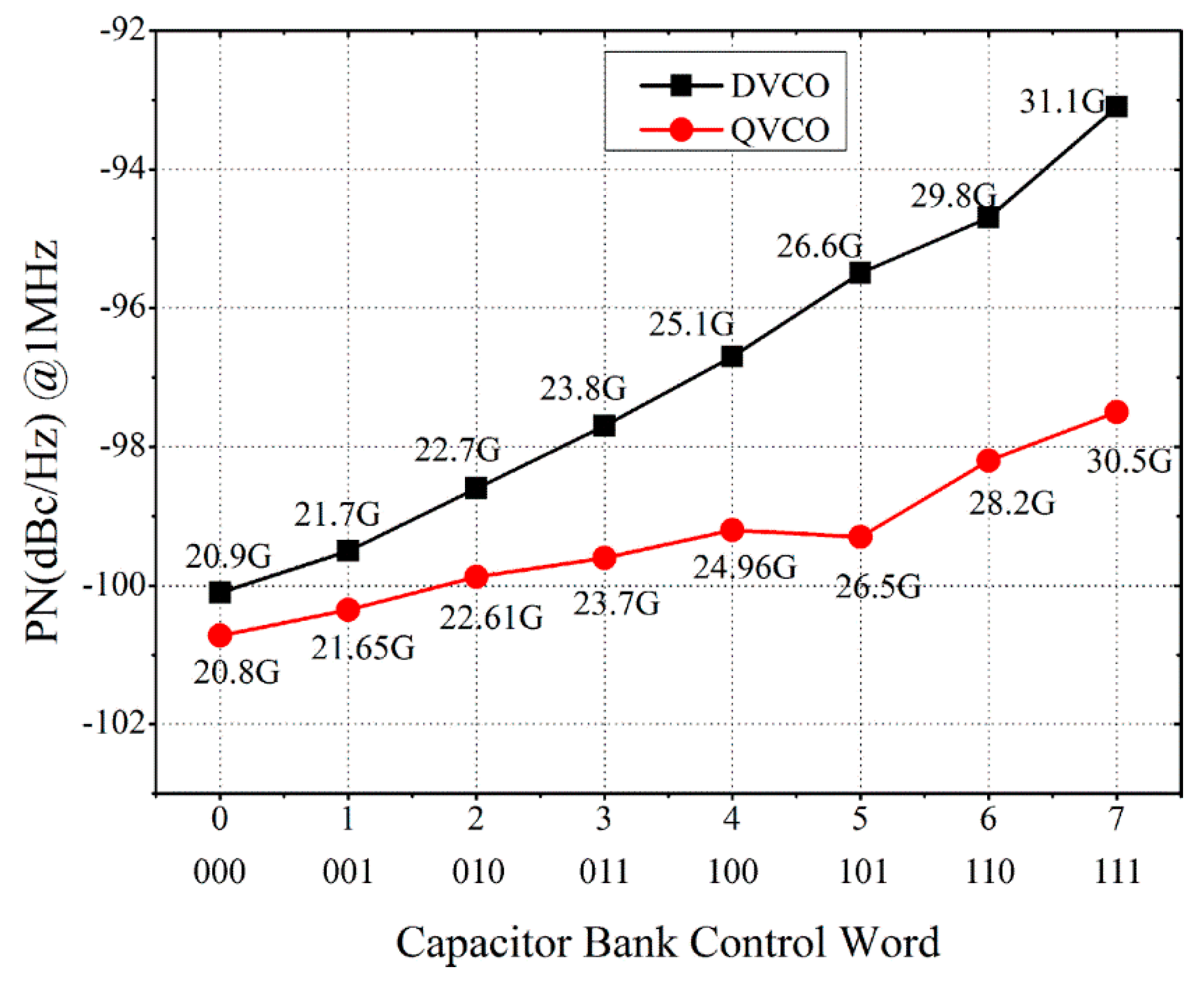
4.1. Differential VCO (DVCO)

A schematic of the proposed differential VCO with integrated wideband varactor circuit is shown in Figure 7. The L C -tank consists of an inductor ( L T a n k = 130 pH), 3-bit switched capacitor bank and the proposed wideband varactor bank. The L C -tank resonator oscillates the desired frequency at the differential output, which is controlled by the control voltage of the varactors ( V c n t r l ) . The fine control provides a continuous change in frequency, whereas the coarse control shifts the continuous characteristic up or down. Fixed capacitance is added between the differential outputs (VCO_P and VCO_N) of the oscillator by the NMOS transistor switches (Sw1, Sw2, Sw3) as shown in Figure 7 [35]. Depending on the gate voltage applied at V C ( n ) / V C ( 0 , 1 , 2 ) , the switches are turned on or off to add the capacitance in or out from the tank. The switches add parasitic resistance when turned on, thereby degrading the P N of the oscillator. Likewise, add parasitic capacitance when turned off, reducing the T R . The D C -biased cross-coupled transistors (T1 and T2) generate the negative transconductance to cancel the parallel tank-resistance to sustain the oscillation. A large biased tail transistor ( T t a i l ) is connected to the common-emitter node ( C N ) of T 1 and T 2 to control current in the circuit.
A differential emitter follower buffer, composed of T 3 and T 4 with the input/output capacitances is connected to the differential output of the oscillators in order to prevent the VCO from the loading effect posed by the external circuitry or measuring equipment. The buffer shown in the schematic provides low output impedance to the instrumentation while measuring the output at the emitter, provided that the VCO output is not adversely affected under load. The buffer capacitances (capacitors between the VCO outputs and T 3 and T 4 ) are carefully selected since these capacitances would add extra parasitic capacitance to the tank and would limit the maximum operating frequency of the VCO. Shown in the proposed VCO schematic, one of the two outputs are terminated with on-chip 50 Ω resistor while the other is left isolated to connect with GSG probe for measurement purpose.
For maximum frequency, the size of the varactor has to be carefully chosen as a trade-off between Q C and capacitance ratio, since the overall quality factor of the tank is affected both by the inductive and capacitive elements as depicted in (3).
1 Q T O T = 1 Q C + 1 Q L
At frequencies <10 GHz, usually, the inductor quality factor ( Q L ) is the major contributor to the overall tank quality factor ( Q T O T ). However, at frequencies >20 GHz, Q of the varactor ( Q C ~ ( ω R s C ) 1 ) also decreases significantly, while that of the inductor ( Q L ~ ( ω L s / R s )) increases with frequency. Also, due to the intrinsic behavior of the varactor, it is difficult to obtain high Q and large C _ m a x / C _ m i n ratio simultaneously to achieve better VCO performance [36]. The proposed varactor circuit to a large extent breaks the “ Q ” and “ C _ m a x / C _ m i n ” trade-off and achieves large capacitance ratio. Keeping “ Q ” and “ C _ m a x / C _ m i n ” trade-off in view, we fixed the varactor size for its optimized performance. In our work, the varactor biasing voltages (Vb1 = 0.4 V, Vb2 = 0.8 V), the capacitance ratio ( C _ m a x / C _ m i n = 3.88 ) branch capacitances (104 fF) and two series inductors, each one of 136 pH are chosen to balance the Q for its widest possible T R at K -band; provided a wider T R from 20 GHz to 31.1 GHz as shown in Figure 8.

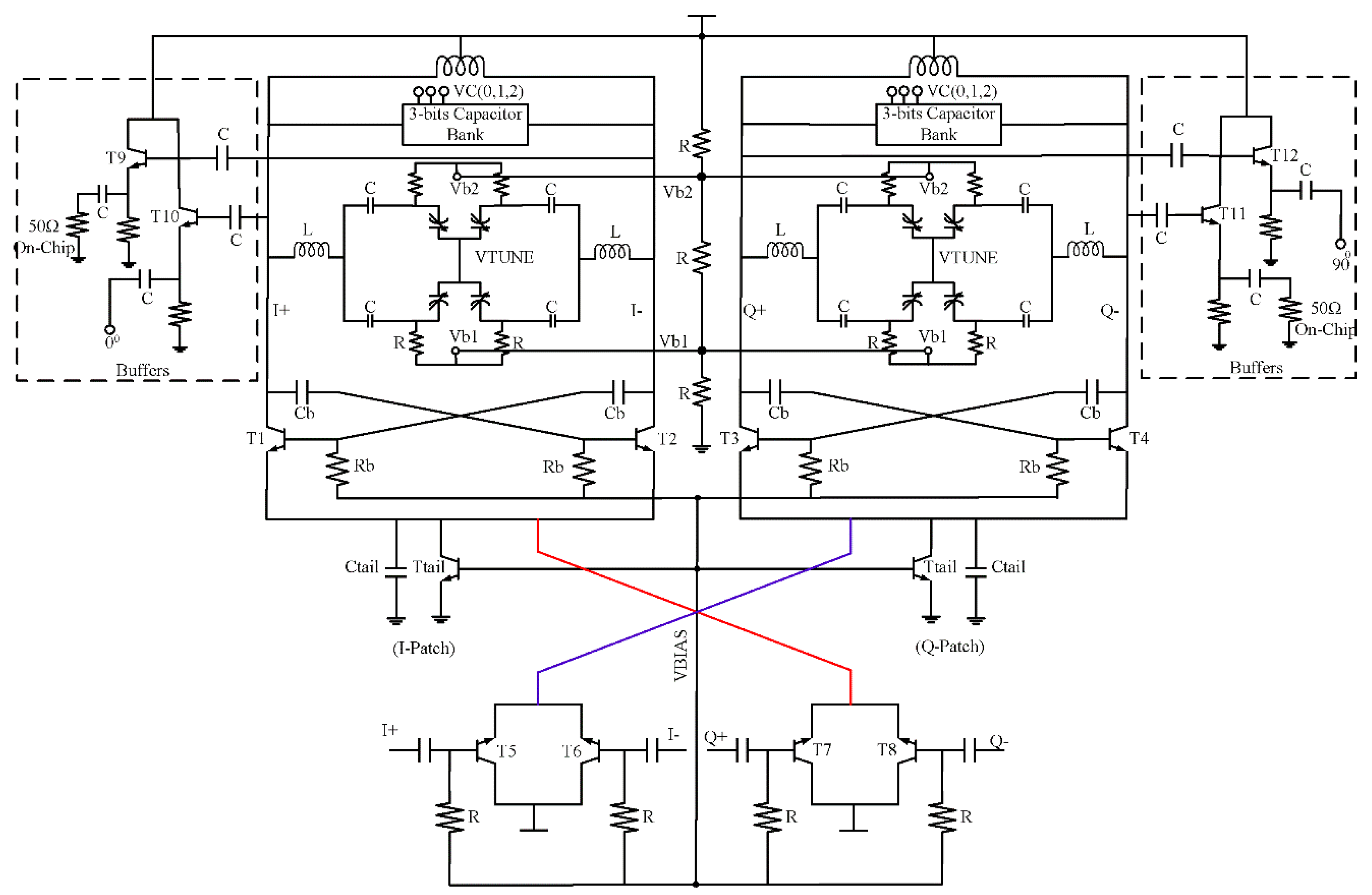
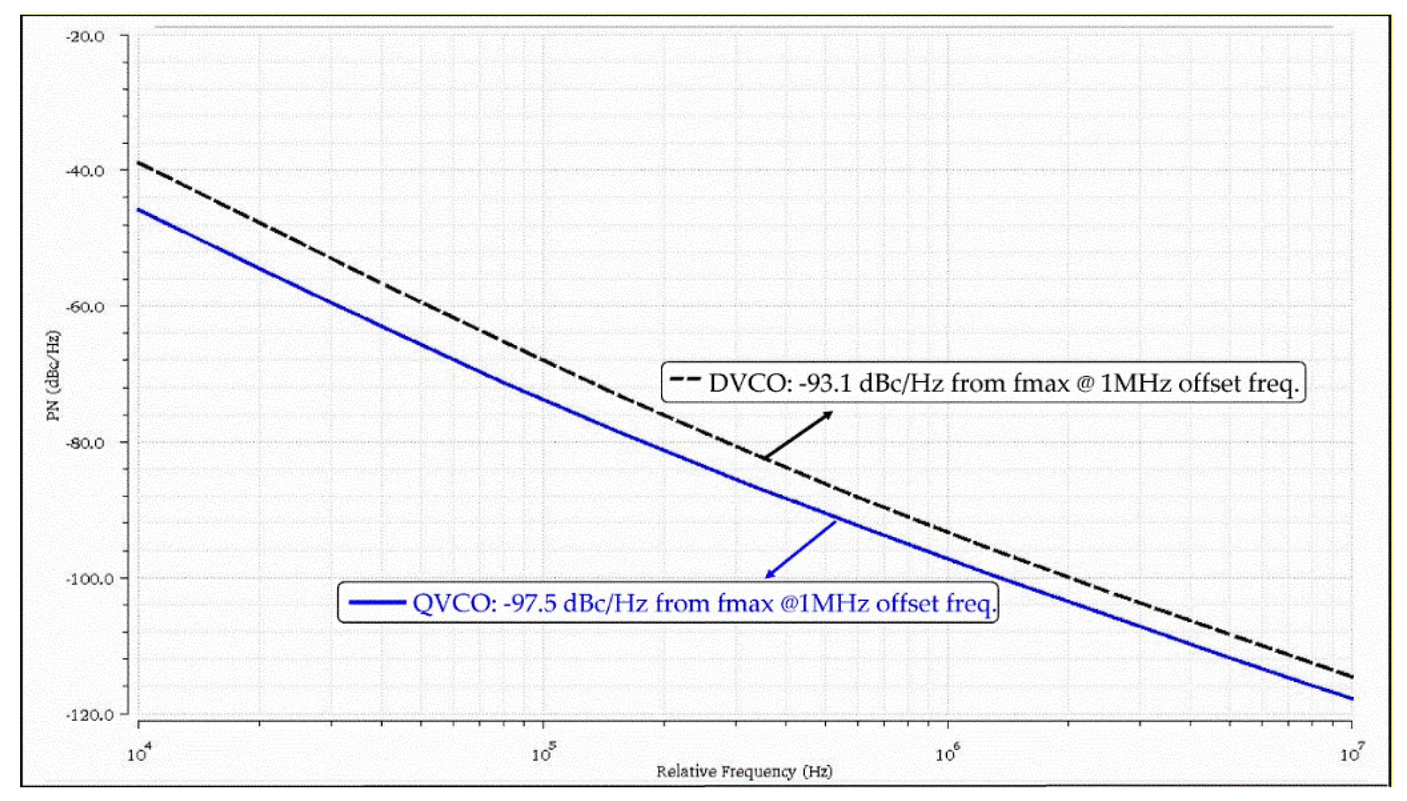
4.2. Quadrature VCO Using Superharmonic Coupling

The proposed Quadrature VCO (QVCO) is designed using the differential VCO presented in Section 4.1. This section presents the quadrature VCO based on superharmonic coupling. Unlike classical L C -QVCOs, this technique cross-injects the 2nd order harmonic at the oscillator common-mode node to enforce the two free-running differential oscillators oscillate in quadrature, i.e., the 2nd order harmonic generated through oscillator 1 using frequency-doubler is injected at the common-mode node of the oscillator 2 and vice versa.
Intrinsically, the cross-coupled L C -VCOs generate the fundamental and 2nd order harmonic frequency components that appear at the differential path and common-mode nodes of the oscillator, respectively. As stated earlier, numerous techniques are proposed to injection-lock the oscillators using fundamental frequency components. Similarly, if an anti-phase relationship between the two oscillators at the 2nd order harmonic is established, then the oscillators can also be locked in quadrature. As an example of superharmonic coupling [11], the two L C -VCOs are locked to oscillate in quadrature when an anti-phase signal with frequency 2 f 0 is injected at the common-mode node of the coupling oscillators. Hence the QVCO can be understood as an injection-locked frequency divider. However, the technique presented in [11] requires an external signal source running at twice the desired frequency. Unlike the injection-locked L C divider presented in [11], this work employs a SiGe HBT frequency doubler designed by taking the fundamental signal at the base of the transistors (T5 toT9) and generate the 2nd harmonic frequency at their common-emitter nodes. The bases of these transistors are A C -coupled and D C -biased with sufficient voltage. In our design, we applied a common bias voltage to all the biasing points in the circuit in order to maintain low power and allow less number of external D C voltage sources.
The output obtained from common-emitter node of the frequency doubler (T5, T6) in oscillator 1 is injected at the common-emitter node of the cross-coupled transistors (T3, T4) of oscillator 2. Similarly, the same connection is made from oscillator 2 to oscillator 1. Thus, if both L C -VCOs are matched, then owing to symmetry their differential outputs have to be in quadrature.
The presented QVCO is composed of two identical VCOs, each one integrated with the proposed wideband varactor circuits. As discussed in Section 3, the fundamental oscillation is available over a significantly wide frequency bandwidth i.e., 20 GHz to 31 GHz. Since the SiGe HBT frequency doubler also senses the fundamental oscillation of the proposed wideband DVCO, the 2nd order harmonic generated by the doubler is also available over a wide frequency range. So, unlike the L C dividers and injection-locked techniques, the proposed oscillator does not suffer from a limited locking range. Schematic of the proposed QVCO is presented in Figure 9.
Using the proposed coupling technique, the post-layout simulated P N of the QVCO demonstrated in Figure 10 is better than its half part. In fact, the P N of the QVCO is always better than DVCO in the entire tuning bandwidth as demonstrated in Figure 11. Here, the PN values are taken from various frequencies interpreted by various combinations of control voltages applied to the capacitor bank. Hence, it can be established that the P N variation in the entire tuning bandwidth is around 7 dB and 3.3 dB and is always less than −93.1 dBc/Hz and −97.5 dB/Hz for DVCO and QVCO, respectively. In addition, the P N is better in lower part of the oscillator’s covered bandwidth and it is deteriorated as the oscillator reaches to its maximum attainable frequency.
To evaluate the performance of the designed oscillators, a widely accepted Figure-of-Merit ( F o M ) is presented in (4).
F o M = L { Δ f } 20 log ( f 0 Δ f ) + 10 log ( P D C 1 m W )
where Δ f , f 0 and P D C are the offset frequency from the carrier, center oscillation frequency and total power, consumed by the core oscillator, respectively.
The F o M is considered to be better with more negative values. In addition to (4), a more widely used expression for F o M is presented to consider the T R of the VCOs as expressed in (5).
F o M T = F o M 20 log ( F T R ( % ) 10 )
where the F T R is “Frequency Tuning Range” covered by the oscillator as the tuning voltage is varied, which is calculated using (6).
F T R ( % ) = ( f m a x f m i n f C e n t e r ) 100 %
f 0 or f C e n t e r is the oscillator center frequency that can be calculated as
f C e n t e r = f m a x + f m i n 2
Getting advantage of wide T R , we calculated F o M with T R ( F o M T ) for fair comparison. Table 1 and Table 2 summarize this work and other state of the art published K / K a band oscillators.

5. Conclusions

In this paper, we presented a wideband differential VCO and superharmonically coupled QVCO, designed and simulated in 130 nm SiGe BiCMOS 8HP process for K -band applications. The proposed bandwidth-enhanced varactor circuit is implemented into the LC-VCO that resulted in wider T R . Further, the quadrature locking is accomplished at the common emitter node of the oscillator using BJT frequency doubler. The proposed quadrature technique exhibited better P N performance than its half circuit. Both designs are realized in class-C for improved P N performance. The designed VCOs can cover >42% tuning bandwidth around 25 GHz oscillation frequency, which is substantially wider than the VCOs operating at comparable frequencies. Among the reported VCOs that have been compared, our VCOs demonstrate a competitive F o M T with the highest tuning bandwidth.

Author Contributions

Conceptualization, F.U. and Y.L.; Data curation, F.U.; Formal analysis, X.W. and M.M.S.; Methodology, F.U.; Project administration, Z.L.; Resources, H.Z.; Supervision, Y.L., Z.L. and H.Z.; Validation, Y.L.; Visualization, X.W.; Writing—original draft, F.U.; Writing—review & editing, F.U. and M.M.S.

Funding

This work was supported by National Science Foundation of China (grant number: 61574165), and CAS-TWAS President’s Fellowship for Farman Ullah (Student ID: 2015A8015908297).

Acknowledgments

The authors would like to thank the Lorentz Solution for Peak View EM Design support.

Conflicts of Interest

The authors declare no conflict of interest.

References

  1. Padovan, F.; Tiebout, M.; Mertens, K.L.R.; Bevilacqua, A.; Neviani, A. Design of low-noise K-band SiGe bipolar VCOs: Theory and Implementation. IEEE Trans. Circuits Syst. Regul. Pap. 2015, 62, 607–615. [Google Scholar] [CrossRef]
  2. Chen, Z.; Wang, M.; Chen, J.X.; Liang, W.F.; Yan, P.P.; Zhai, J.F.; Hong, W. Linear CMOS LC-VCO Based on triple-coupled inductors and its application to 40-GHz phase-locked loop. IEEE Trans. Microw. Theory Tech. 2017, 65, 2977–2989. [Google Scholar] [CrossRef]
  3. Chang, H.Y.; Chiu, Y.T. K-Band CMOS differential and quadrature voltage-controlled oscillators for low phase-noise and low-power applications. IEEE Trans. Microw. Theory Tech. 2012, 60, 46–59. [Google Scholar] [CrossRef]
  4. Yang, J.; Kim, C.Y.; Kim, D.W.; Hong, S. Design of a 24-GHz CMOS VCO with an asymmetric-width transformer. IEEE Trans. Circuits Syst. Express Briefs 2010, 57, 173–177. [Google Scholar] [CrossRef]
  5. Kucharski, M.; Herzel, F.; Ng, H.J.; Kissinger, D. A Ka-band BiCMOS LC-VCO with wide tuning range and low phase noise using switched coupled inductors. In Proceedings of the 2016 11th European IEEE Conference of Microwave Integrated Circuits Conference (EuMIC), London, UK, 3–4 October 2016; pp. 201–204. [Google Scholar]
  6. Li, C.C.; Wang, T.P.; Kuo, C.C.; Chuang, M.C.; Wang, H. A 21 GHz complementary transformer coupled CMOS VCO. IEEE Microw. Wirel. Compon. Lett. 2008, 18, 278–280. [Google Scholar]
  7. Hsieh, C.K.; Kao, K.Y.; Tseng, J.R.; Lin, K.Y. A K-Band CMOS low power modified colpitts VCO using transformer feedback. In Proceedings of the 2009 IEEE MTT-S International Microwave Symposium Digest, Boston, MA, USA, 7–12 June 2009; pp. 1293–1296. [Google Scholar]
  8. Kuo, Y.H.; Jeng-Han, T.; Huang, T.W. In A 1.7-mw, 16.8% frequency tuning, 24-GHz transformer-based lc-vco using 0.18µm CMOS technology. In Proceedings of the 2009 IEEE Conference of Radio Frequency Integrated Circuits Symposium, Boston, MA, USA, 7–9 June 2009; pp. 79–82. [Google Scholar]
  9. Lee, W.; Lee, S.; Choi, J.; So, J.; Kwon, Y. Ka-band VCO with parasitic capacitance cancelling technique. Electron. Lett. 2016, 53, 38–40. [Google Scholar] [CrossRef]
  10. Wu, Q.; Quach, T.K.; Mattamana, A.; Elabd, S.; Orlando, P.L.; Dooley, S.R.; McCue, J.J.; Creech, G.L.; Khalil, W. Frequency tuning range extension in LC-VCOs using negative-capacitance circuits. IEEE Trans. Circuits Syst. Express Briefs 2013, 60, 182–186. [Google Scholar] [CrossRef]
  11. Mazzanti, A.; Uggetti, P.; Svelto, F. Analysis and design of injection-locked LC dividers for quadrature generation. IEEE J. Solid-State Circuits 2004, 39, 1425–1433. [Google Scholar] [CrossRef]
  12. Crols, J.; Steyaert, M.S.J. A single-chip 900 MHz CMOS receiver front-end with a high performance low-if topology. IEEE J. Solid-State Circuits 1995, 30, 1483–1492. [Google Scholar] [CrossRef]
  13. Törmänen, M.; Sjoland, H. A 24-ghz LC-QVCO in 130-nm CMOS using 4-bit switched tuning. In Proceedings of the 2008 IEEE Conference of International Conference on Microelectronics (ICM), Sharjah, UAE, 14–17 December 2008; pp. 421–424. [Google Scholar]
  14. Andreani, P.; Xiaoyan, W. On the phase-noise and phase-error performances of multiphase LC CMOS VCOs. IEEE J. Solid-State Circuits 2004, 39, 1883–1893. [Google Scholar] [CrossRef] [Green Version]
  15. Lee, S.Y.; Wang, L.H.; Lin, Y.H. A CMOS quadrature VCO with subharmonic and injection-locked techniques. IEEE Trans. Circuits Syst. Express Briefs 2010, 57, 843–847. [Google Scholar] [CrossRef]
  16. Hancock, T.M.; Rebeiz, G.M. A novel superharmonic coupling topology for quadrature oscillator design at 6 GHz. In Proceedings of the 2004 IEEE Conference of Radio Frequency Integrated Circuits (RFIC) Systems, Forth Worth, TX, USA, 6–8 June 2004; pp. 285–288. [Google Scholar]
  17. Hye-Ryoung, K.; Choong-Yul, C.; Seung-Min, O.; Moon-Su, Y.; Sang-Gug, L. A very low-power quadrature VCO with back-gate coupling. IEEE J. Solid-State Circuits 2004, 39, 952–955. [Google Scholar] [CrossRef]
  18. Yi, X.; Liang, Z.; Feng, G.; Boon, C.C.; Meng, F. A 93.4-to-104.8 GHz 57 mW fractional-N cascaded sub-sampling PLL with true in-phase injection-coupled QVCO in 65 nm CMOS. In Proceedings of the 2016 IEEE Conference of Radio Frequency Integrated Circuits Symposium (RFIC), San Francisco, CA, USA, 22–24 May 2016; pp. 122–125. [Google Scholar]
  19. Yun, S.-J.; Yoon, D.-Y.; Lee, S.-G. A complementary-coupled CMOS LC quadrature oscillator. IEICE Trans. Electron. 2008, 91, 1806–1810. [Google Scholar] [CrossRef]
  20. Gierkink, S.L.J.; Levantino, S.; Frye, R.C.; Samori, C.; Boccuzzi, V. A low-phase-noise 5-GHz CMOS quadrature VCO using superharmonic coupling. IEEE J. Solid-State Circuits 2003, 38, 1148–1154. [Google Scholar] [CrossRef]
  21. Xi, T.; Guo, S.; Gui, P.; Zhang, J.; Kenneth, Κ.O.; Fan, Y.; Huang, D.; Gu, R.; Morgan, M. Low-phase-noise 54 GHz quadrature VCO and 76GHz/90GHz VCOs in 65 nm CMOS process. In Proceedings of the 2014 IEEE Conference of Radio Frequency Integrated Circuits Symposium, Tampa, FL, USA, 1–3 June 2014; pp. 257–260. [Google Scholar]
  22. Choul-Young, K.; Jaemo, Y.; Dong-Wook, K.; Songcheol, H. A K-band quadrature VCO based on asymmetric coupled transmission lines. In Proceedings of the 2008 IEEE Conference of MTT-S International Microwave Symposium Digest, Atlanta, GA, USA, 15–20 June 2008; pp. 363–366. [Google Scholar]
  23. Mingquan, B.; Yinggang, L.; Jacobsson, H. A 25-GHz ultra-low phase noise lnGap/GaAs HBT VCO. IEEE Microw. Wirel. Compon. Lett. 2005, 15, 751–753. [Google Scholar] [CrossRef]
  24. Shin, H.; Kim, J. A 17-GHz Push-Push VCO based on output extraction from a capacitive common node in GaInp/GaAs HBT technology. IEEE Trans. Microw. Theory Tech. 2006, 54, 3857–3863. [Google Scholar] [CrossRef]
  25. Chang, H.Y.; Lin, C.H.; Liu, Y.C.; Yeh, Y.L.; Chen, K.; Wu, S.H. 65-nm CMOS dual-gate device for ka-band broadband low-noise amplifier and high-accuracy quadrature voltage-controlled oscillator. IEEE Trans. Microw. Theory Tech. 2013, 61, 2402–2413. [Google Scholar] [CrossRef]
  26. Tormanen, M.; Sjoland, H. A 26-GHz LC-QVCO in 0.13-μm CMOS. In Proceedings of the 2007 IEEE Conference of Asia Pasific Microwave Conference (APMC), Bangkok, Thailand, 11–14 December 2007; pp. 1–4. [Google Scholar]
  27. Mazzanti, A.; Andreani, P. Class-C harmonic CMOS VCOs, with a general result on phase noise. IEEE J. Solid-State Circuits 2008, 43, 2716–2729. [Google Scholar] [CrossRef]
  28. Fanori, L.; Andreani, P. Highly efficient class-C CMOS VCOs, including a comparison with class-B VCOs. IEEE J. Solid-State Circuits 2013, 48, 1730–1740. [Google Scholar] [CrossRef]
  29. Fard, A.; Andreani, P. An analysis of 1/f2 phase noise in bipolar colpitts oscillators (with a digression on bipolar differential-Pair oscillators). IEEE J. Solid-State Circuits 2007, 42, 374–384. [Google Scholar] [CrossRef]
  30. Boscolo, F.; Padovan, F.; Quadrelli, F.; Tiebout, M.; Neviani, A.; Bevilacqua, A. A 21GHz 20.5%-tuning range colpitts VCO with -119 dBc/Hz phase noise at 1MHz offset. In Proceedings of the 2017 43rd IEEE European Solid State Circuits Conference (ESSCIRC), Leuven, Belgium, 11–14 September 2017; pp. 91–94. [Google Scholar]
  31. Yamashita, F.; Matsuoka, T.; Kihara, T.; Takobe, I.; Park, H.-J.; Taniguchi, K. Analytical design of a 0.5V 5GHz CMOS LC-VCO. IEICE Electron. Express 2009, 6, 1025–1031. [Google Scholar] [CrossRef] [Green Version]
  32. Razavi, B.; Behzad, R. RF Microelectronics, 2nd ed.; Prentice Hall Press: New York, NY, USA, 2011. [Google Scholar]
  33. Andreani, P.; Mattisson, S. On the Use of MOS Varactors in RF VCO’s. IEEE J. Solid-State Circuits 2000, 35, 905–910. [Google Scholar] [CrossRef]
  34. Fox-Turnbull, W.H. Design and Technology Support Education; GlobalFoundries: Santa Clara, CA, USA, 2016. [Google Scholar]
  35. Kamata, T.; Matsuoka, T.; Taniguchi, K. RF Front-end Design for CMOS Terrestrial Wideband TV Tuner IC. IEEE Trans. Consum. Electron. 2010, 56, 1340–1348. [Google Scholar] [CrossRef]
  36. Changhua, C.; Kenneth, K.O. Millimeter-wave voltage-controlled oscillators in 0.13 µm CMOS technology. IEEE J. Solid-State Circuits 2006, 41, 1297–1304. [Google Scholar]
Figure 1. Standard schematics of (a) class-C and (b) differential Colpitts oscillators.
Electronics 07 00127 g001
Figure 2. Schematics of (a) tank-coupled p-n diode, (b) n-type A-MOS varactor cross-section and its corresponding schematic view for differential applications.
Electronics 07 00127 g002
Figure 3. Schematics of the (a) conventional and (b) proposed wideband varactor with parasitics highlighted.
Electronics 07 00127 g003
Figure 4. Simulated single frequency tuning characteristic using conventional and proposed varactors.
Electronics 07 00127 g004
Figure 5. Distributed Biasing of the varactor bank.
Electronics 07 00127 g005
Figure 6. Physical layouts of the designed oscillators.
Electronics 07 00127 g006
Figure 7. Complete schematic of a Differential Voltage Controlled Oscillator (DVCO) incorporated with proposed wideband varactor circuit.
Electronics 07 00127 g007
Figure 8. Voltage Controlled Oscillator (VCO) output frequency as a function of the capacitor bank control word.
Electronics 07 00127 g008
Figure 9. A simplified schematic of the superharmonically coupled Quadrature Voltage Controlled Oscillator (QVCO) with proposed wideband varactor circuits.
Electronics 07 00127 g009
Figure 10. P N plot of DVCO and QVCO at an offset range from 10 KHz to 10 MHz highlighting P N s from their corresponding maximum carriers.
Electronics 07 00127 g010
Figure 11. P N plot of DVCO and QVCO at 1 MHz offset frequency in the entire T R , representing oscillation frequency taken at various capacitor bank control word.
Electronics 07 00127 g011
Table 1. Comparison of reported K / K a band DVCOs and this work.
Ref. f 0
(GHz)
P N @1 MHz
(dBc/Hz)
P D C
(mW)
F T R
(%)
F o M T Process
[1]22.7−1141817−193SiGe HBT
[2]20.85−100.78.115.8−181.890 nm CMOS
[3]20.8−116.434.8−191.690 nm CMOS
[4]24.27−100.337.82.2−1790.18 µm CMOS
[5]32.55−971918.1−1800.13 um SiGe BiCMOS
[6]21.5−1131304.6−171.80.25 um SiGe
[7]23−10042−1810.13 µm CMOS
[8]24.5−95.51.716.8−185.40.18 µm CMOS
[10]40−951227−184.90.13 µm CMOS
[30]21−1197020−194SiGe BiCMOS
Our Work25.5−961243−1860.13 um SiGe BiCMOS
Table 2. Comparison of reported K / K a band QVCOs and this work.
Ref.Coupling Method f 0
(GHz)
P N @1 MHz
(dBc/Hz)
P D C
(mW)
F T R
(%)
F o M T I/Q ErrorProcess
[3]Series20.9−117.26.33.1−185.4n/a90 nm CMOS
[13]Parallel24.7−111.6244.3−186n/a0.13 µm CMOS
[21]Transformer Coupled20−111.6740.3210.4−181.51.5°0.18 µm CMOS
[22]Transmission Line33−992.64-−183.7n/a0.12 µm SiGe HBT
[25]Series25.3−10914.42.81−185.51.8°65 nm CMOS
[26]Parallel26.1−114243−188.5n/a0.13 µm CMOS
Our WorkSuperharmonic Coupling25.3−99.22542−185.81.2°0.13 µm SiGe BiCMOS

