Analysis and Suppression of Unwanted Turn-On and Parasitic Oscillation in SiC JFET-Based Bi-Directional Switches

 ,
,
Abstract
:1. Introduction
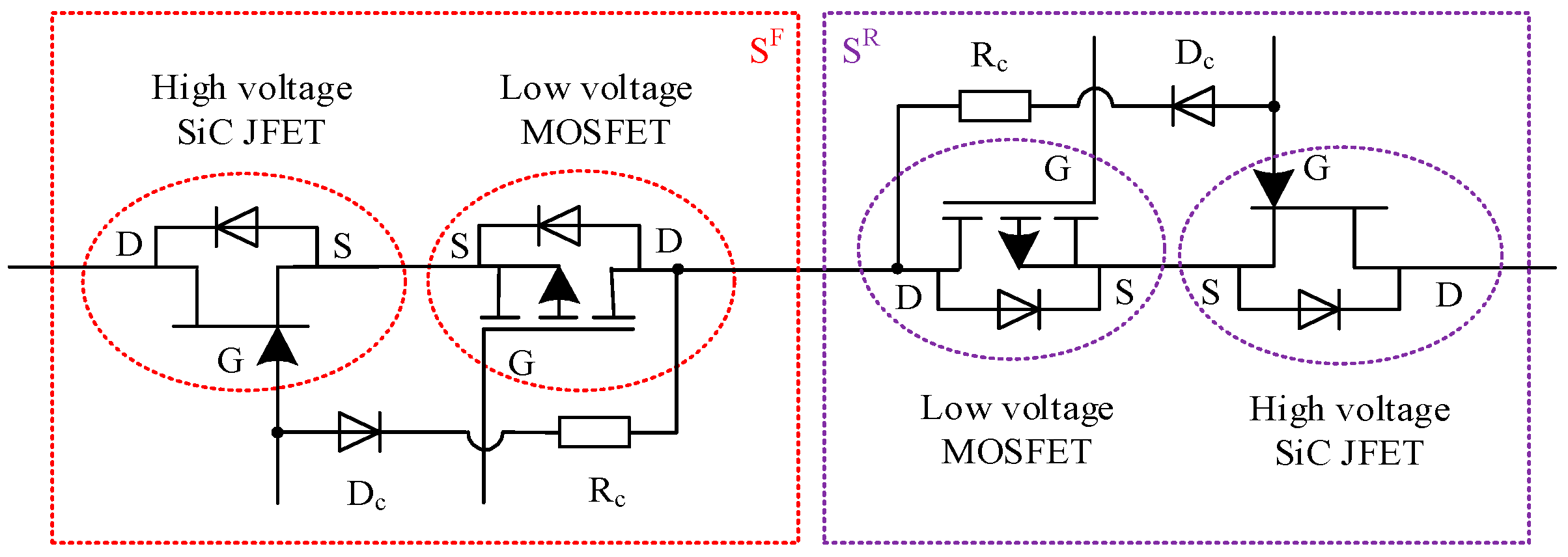
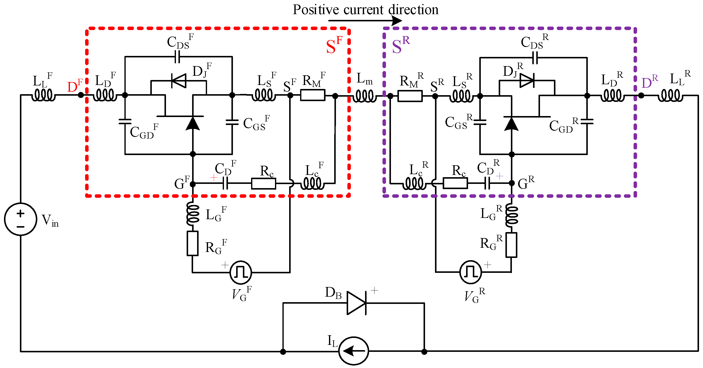
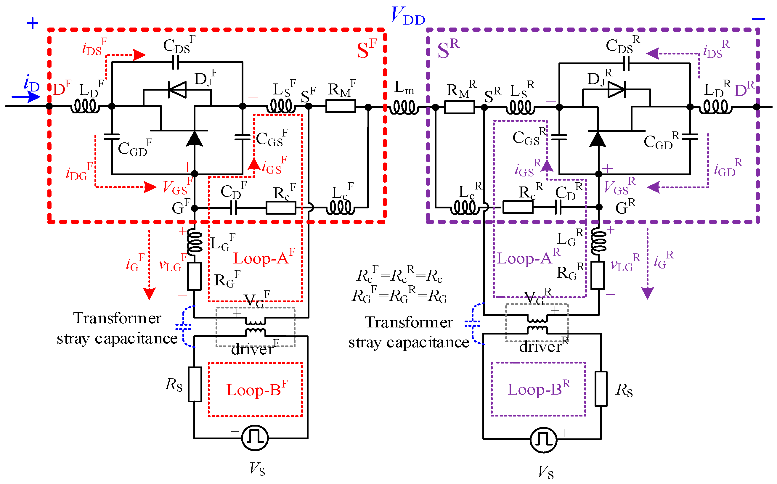
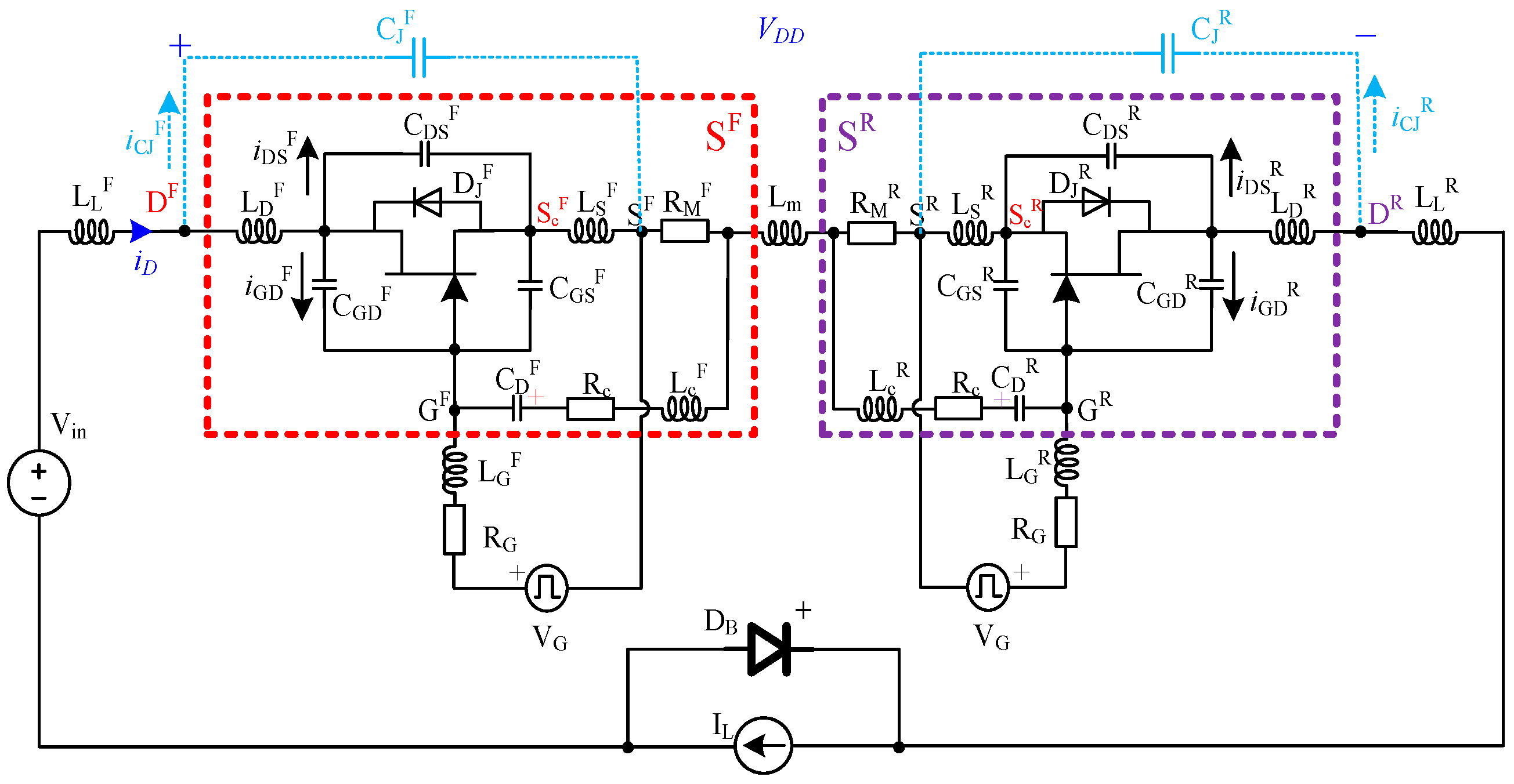
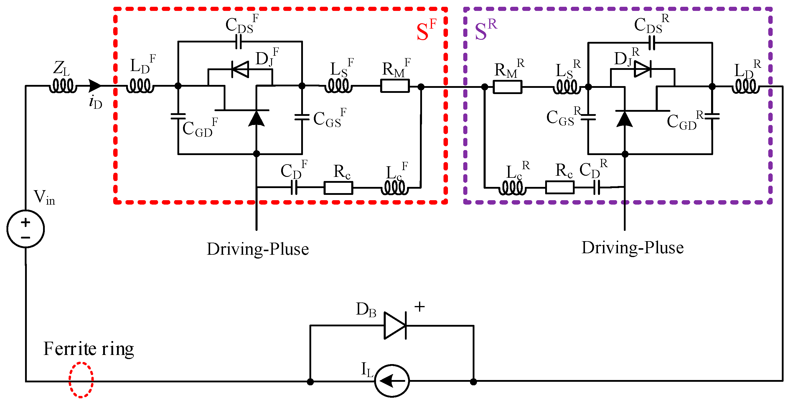
2. The Developed Configuration of the SiC JFET-Based BDS
3. Analysis and Suppression of UTO
3.1. Root Cause Analysis of UTO
3.2. UTO Suppression
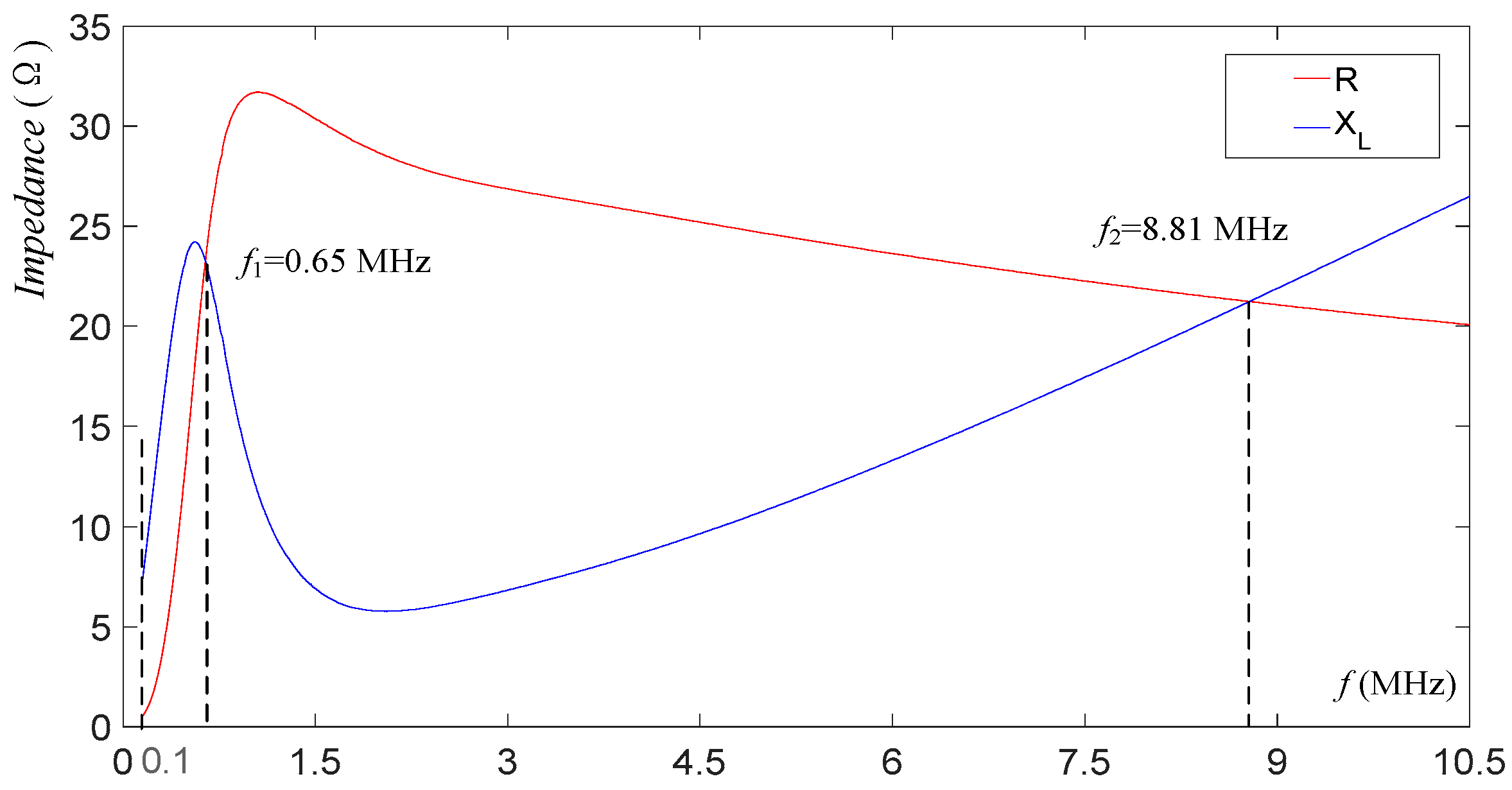
4. Parasitic Oscillation Suppression
4.1. Effect of Adding a Snubber Capacitor on Parasitic Oscillation during Turn-Off Transient
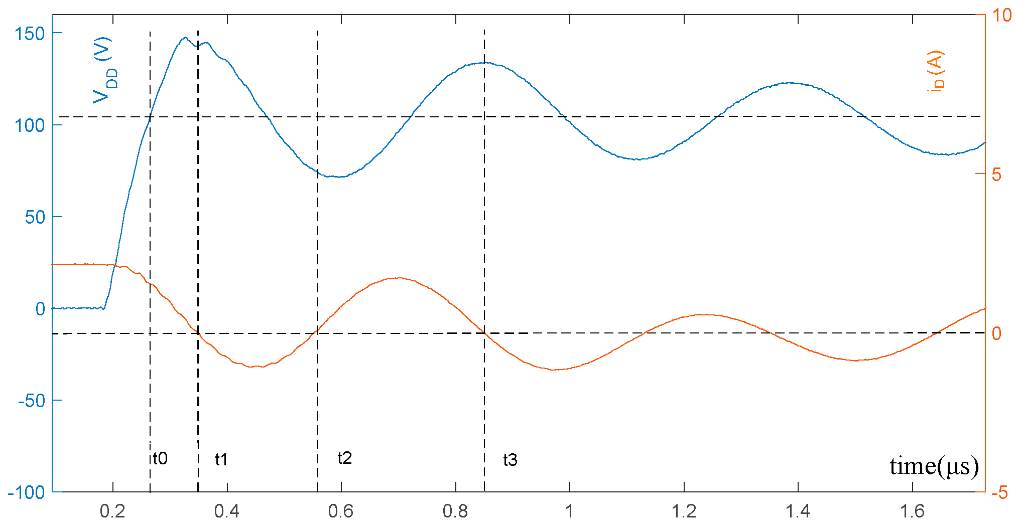
4.1.1. Stage I: BDS Drain–Drain Voltage Rising
4.1.2. Stage II: BDS Drain–Drain Voltage Falling
4.2. Effect of Adding a Ferrite Ring on Parasitic Oscillation during Turn-On Transient
4.3. Combined Effects of the Snubber Capacitor and the Ferrite Ring
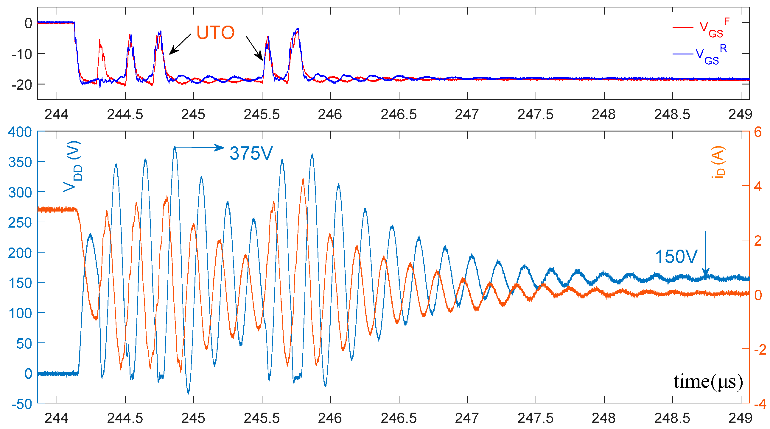
5. Relationship between UTO and Parasitic Oscillation
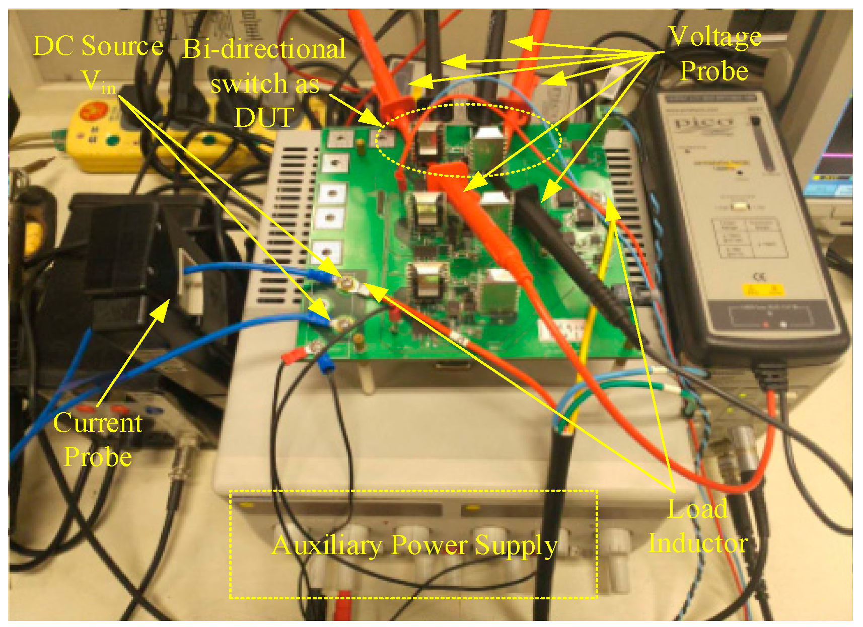
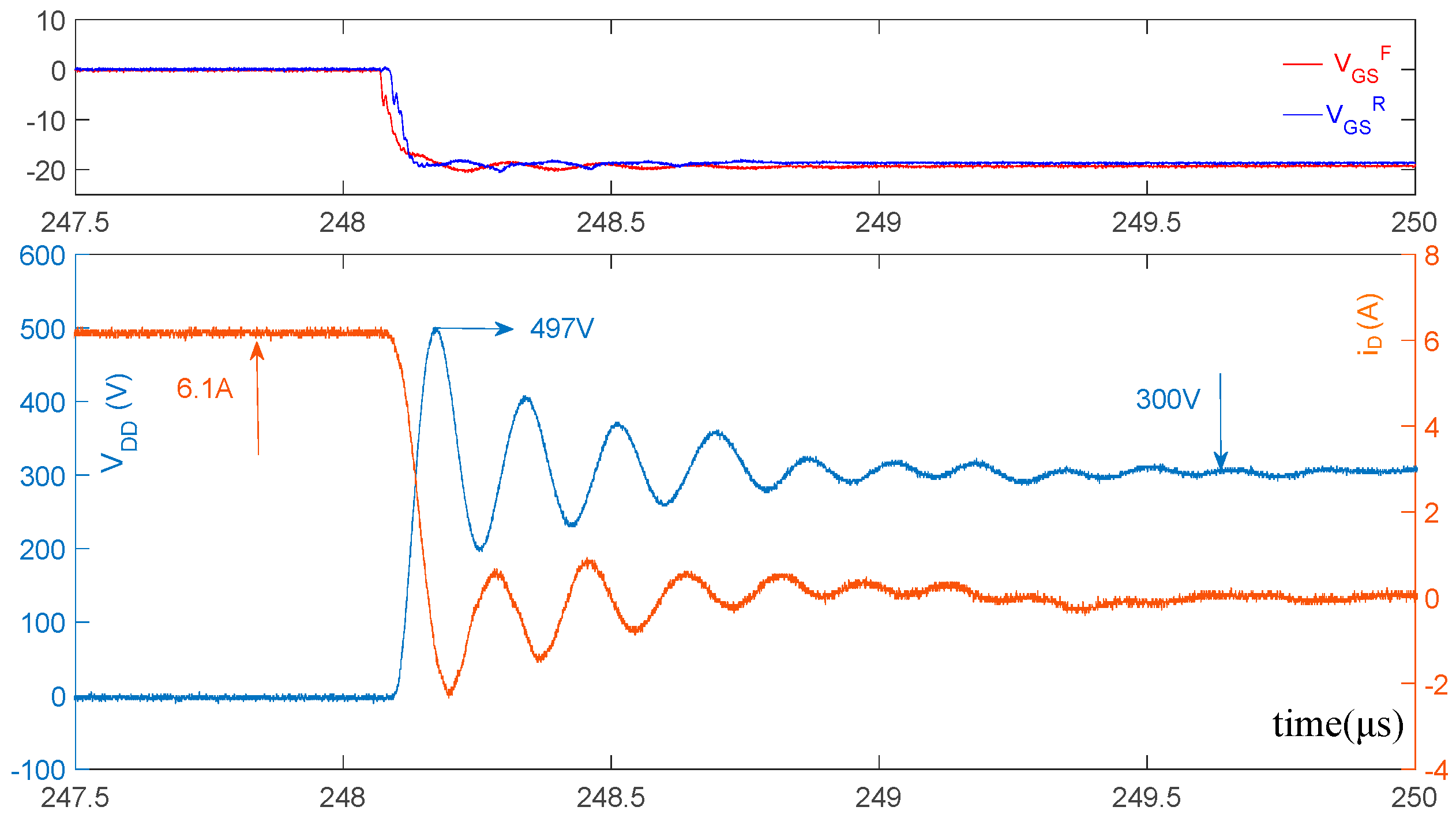
6. Experimental Result and Discussion
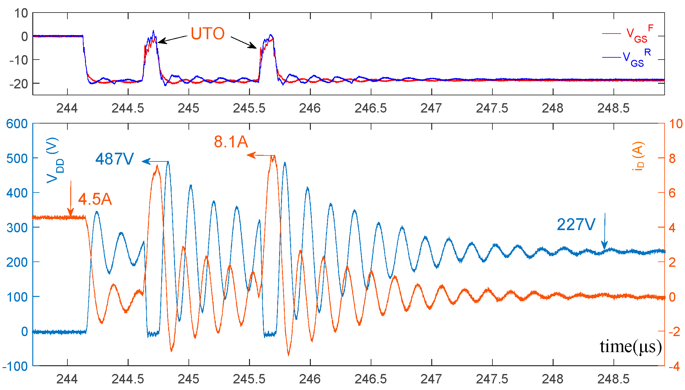
6.1. Mitigation of UTO
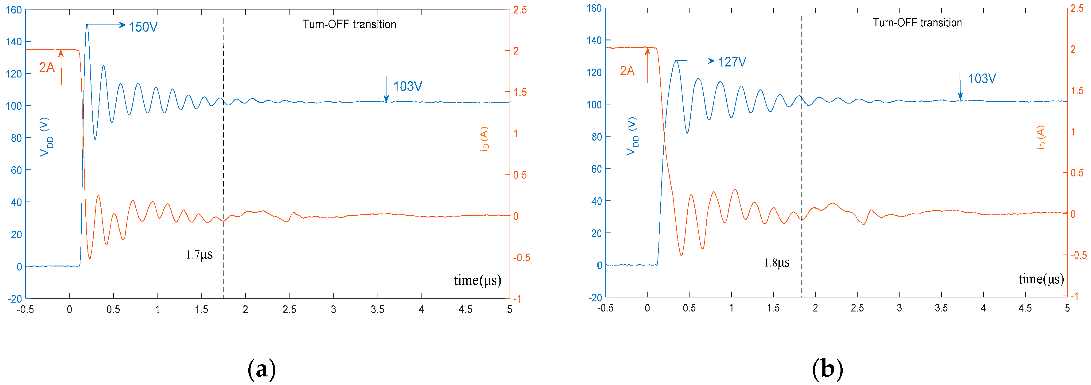
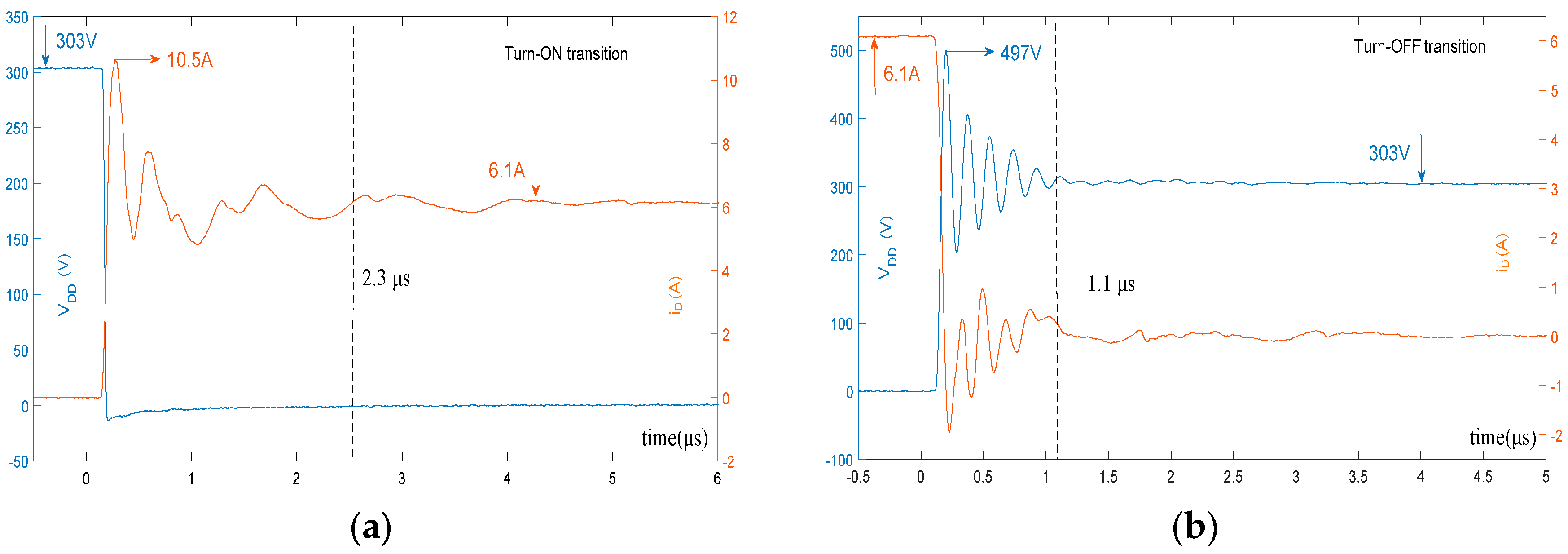
6.2. Impact of the Snubber Capacitor on the Turn-off Behavior
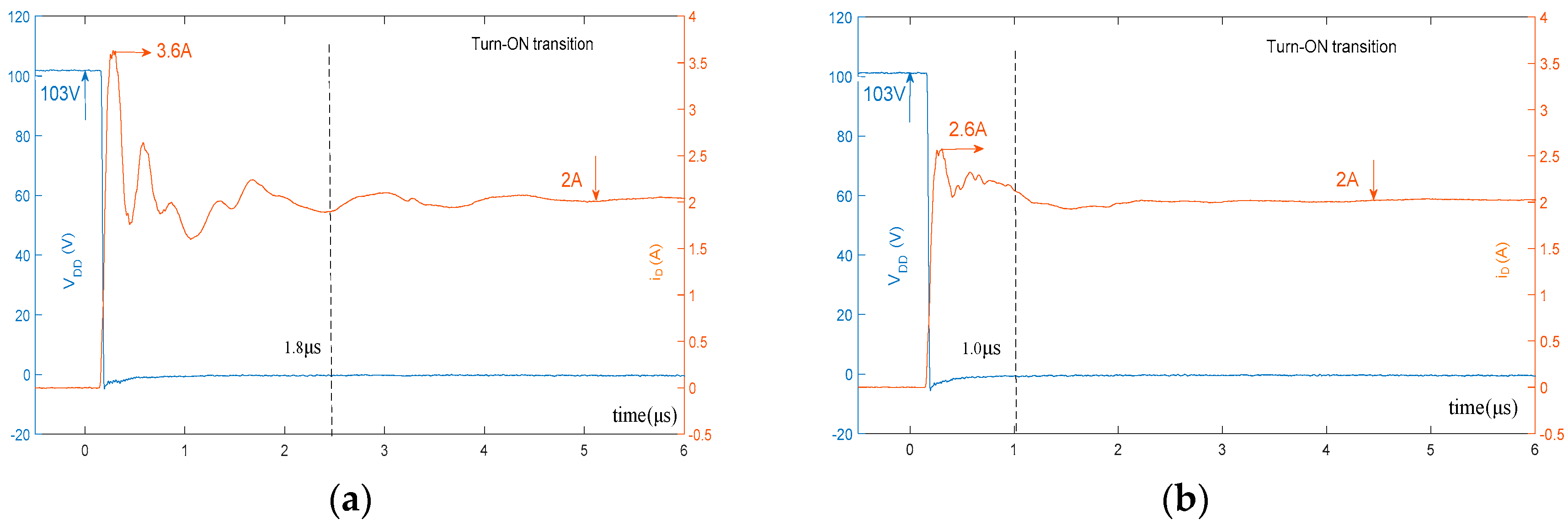
6.3. Impact of the Ferrite Ring on the Turn-On Behavior
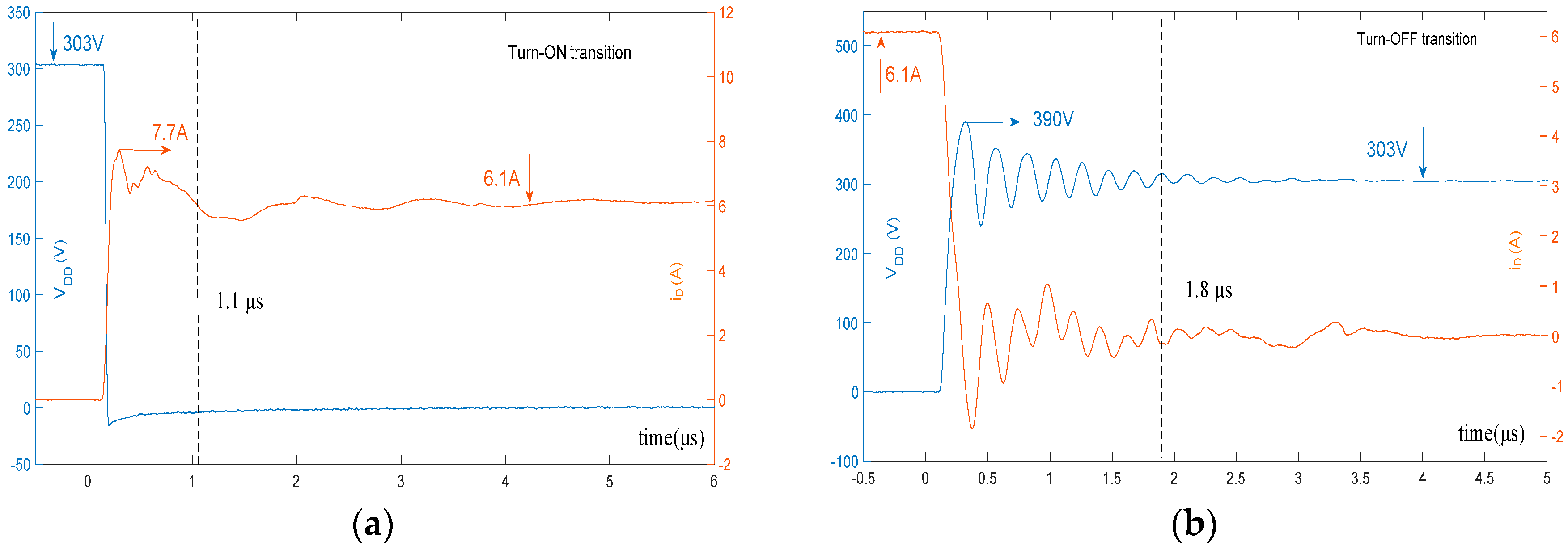
6.4. Combined Effects of the Snubber Capacitor and the Ferrite Ring
7. Conclusions
Author Contributions
Funding
Conflicts of Interest
References
- Camacho, A.P.; Sala, V.; Ghorbani, H.; Martinez, J.L.R. A novel active gate driver for improving SiC MOSFET switching trajectory. IEEE Trans. Ind. Electron. 2017, 64, 9032–9042. [Google Scholar] [CrossRef]
- Liu, T.; Ning, R.; Wong, T.T.; Shen, Z.J. Modeling and analysis of SiC MOSFET switching oscillations. IEEE J. Emerg. Sel. Top. Power Electron. 2016, 4, 747–756. [Google Scholar] [CrossRef]
- Lemmon, A.; Mazzola, M.; Gafford, J.; Parker, C. Instability in half-bridge circuits switched with wide band-gap transistors. IEEE Trans. Power Electron. 2014, 29, 2380–2392. [Google Scholar] [CrossRef]
- Lemmon, A.; Mazzola, M.; Gafford, J.; Parker, C. Stability considerations for silicon carbide field-effect transistors. IEEE Trans. Power Electron. 2013, 28, 4453–4459. [Google Scholar] [CrossRef]
- Jahdi, S.; Alatise, O.; Gonzalez, J.A.O.; Bonyadi, R.; Ran, L.; Mawby, P. Temperature and switching rate dependence of crosstalk in Si-IGBT and SiC power modules. IEEE Trans. Ind. Electron. 2016, 63, 849–863. [Google Scholar] [CrossRef]
- Velander, E.; Löfgren, A.; Kretschmar, K.; Nee, H.P. Novel solutions for suppressing parasitic turn-on behaviour on lateral vertical JFETs. In Proceedings of the 16th European Conference on Power Electronics and Applications, Lappeenranta, Finland, 26–28 August 2014; pp. 1–8. [Google Scholar]
- Heer, D.; Bayerer, R.; Domes, D. SiC-JFET in half-bridge configuration-parasitic turn-on at current commutation. In Proceedings of the International Exhibition and Conference for Power Electronics, Intelligent Motion, Renewable Energy and Energy Management (PCIM), Nuremberg, Germany, 19–20 May 2014; pp. 1–8. [Google Scholar]
- Miao, Z.; Wang, C.M.; Ngo, K.D. Simulation and characterization of cross-turn-on inside a power module of paralleled SiC MOSFETs. IEEE Trans. Compon. Packag. Manuf. Technol. 2017, 7, 186–192. [Google Scholar] [CrossRef]
- Ahmed, M.R.; Todd, R.; Forsyth, A.J. Predicting SiC MOSFET behavior under hard-switching, soft-Switching, and false turn-on conditions. IEEE Trans. Ind. Electron. 2017, 64, 9001–9011. [Google Scholar] [CrossRef]
- Zhang, W.; Zhang, Z.; Wang, F.; Costinett, D.; Tolbert, L.; Blalock, B. Common source inductance introduced self-turn-on in MOSFET turn-off transient. In Proceedings of the Applied Power Electronics Conference and Exposition (APEC), Tampa, FL, USA, 26–30 March 2017; pp. 837–842. [Google Scholar]
- Nayak, P.; Hatua, K. Parasitic Inductance and capacitance-assisted active gate driving technique to minimize switching loss of SiC MOSFET. IEEE Trans. Ind. Electron. 2017, 64, 8288–8298. [Google Scholar] [CrossRef]
- Kim, J.; Shin, D.; Sul, S.K. A damping scheme for switching ringing of full SiC MOSFET by air core PCB circuit. IEEE Trans. Power Electron. 2017, 33, 4605–4615. [Google Scholar] [CrossRef]
- Huang, X.; Du, W.; Lee, F.C.; Li, Q.; Zhang, W. Avoiding divergent oscillation of a cascode GaN device under high-current turn-off condition. IEEE Trans. Power Electron. 2017, 32, 593–601. [Google Scholar] [CrossRef]
- Josifović, I.; Popović-Gerber, J.; Ferreira, J.A. Improving SiC JFET switching behavior under influence of circuit parasitics. IEEE Trans. Power Electron. 2012, 27, 3843–3854. [Google Scholar] [CrossRef]
- Saadeh, M.; Chinthavali, M.S.; Ozpineci, B.; Mantooth, H.A. Anti-series normally-On SiC JFETs operating as bidirectional switches. In Proceedings of the Energy Conversion Congress and Exposition (ECCE 2013), Denver, CO, USA, 15–19 September 2013; pp. 2892–2897. [Google Scholar]
- Wang, L.; Zhang, X.; Deng, J.; Yang, J.; Oladele, O.K.; Zhao, Y. Unwanted turn-on of SiC JFET bi-directional switches under influence of parasitic parameters. In Proceedings of the 43rd Industrial Electronics Society (IECON 2017), Beijing, China, 29–30 October 2017; pp. 4194–4199. [Google Scholar]
- Santi, E.; Peng, K.; Mantooth, H.A.; Hudgins, J.L. Modeling of wide-bandgap power semiconductor devices—Part II. IEEE Trans. Electron Devices 2015, 62, 434–442. [Google Scholar] [CrossRef]
- Siemieniec, R.; Kirchner, U. The 1200V direct-driven SiC JFET power switch. In Proceedings of the 14th European Conference on Power Electronics and Applications, Birmingham, UK, 30–31 August 2011; pp. 1–10. [Google Scholar]
- Infienon Chip, 1EDI30J12CP Single JFET Driver IC. Available online: https://www.infineon.com/cms/en/product/power/gate-driver-ics/galvanic-isolated-gate-driver/1edi30j12cp/ (accessed on 12 November 2014).
- Application Note AN2013-17 EiceDRIVER™ Enhanced 1EDI30J12Cx. Available online: https://www.infineon.com/cms/en/search.html#!view=downloads&term=EiceDRIVER%E2%84%A2#32Enhanced#321EDI30J12Cx/ (accessed on 16 December 2013).
- Huang, X.; Li, Q.; Liu, Z.; Lee, F.C. Analytical loss model of high voltage GaN HEMT in cascode configuration. IEEE Trans. Power Electron. 2014, 29, 2208–2219. [Google Scholar] [CrossRef]
- Infienon Chip, 5th Generation thinQ!™ 1200 V SiC Schottky Diode IDH16G120C5. Available online: https://www.infineon.com/cms/en/product/power/silicon-carbide-sic/coolsic-schottky-diode/idh16g120c5/ (accessed on 21 July 2017).
- RIGAL. DG1022 Double Channel Function/Arbitrary Waveform Generator. Available online: http://www.rigol.com/ (accessed on 15 January 2010).
- Fereidoony, F.; Mirtaheri, S.A.; Chamaani, S. High-resolution range estimation using time delays in ultra-wideband M-sequence radar. IET Microw. Antennas Propag. 2017, 11, 1332–1339. [Google Scholar] [CrossRef]
- Wang, Q.; Krautschneider, W.H.; Weber, W.; Schmitt-Landsiedel, D. Influence of MOSFET IV characteristics on switching delay time of CMOS inverters after hot-carriers stress. IEEE Electron Device Lett. 1991, 12, 238–240. [Google Scholar] [CrossRef]


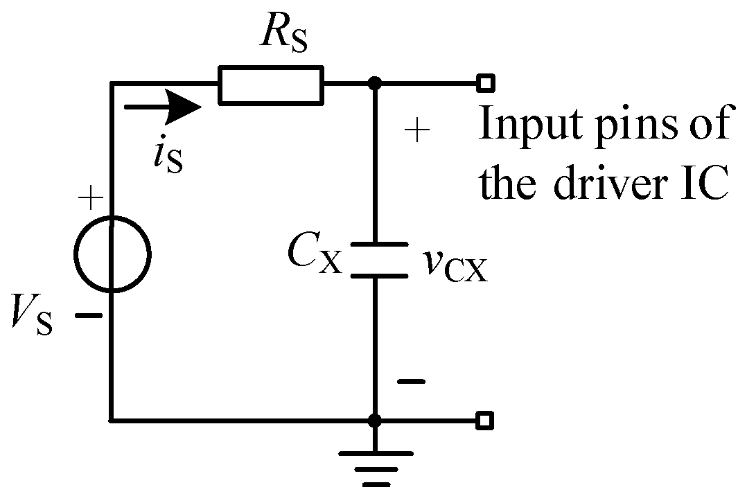
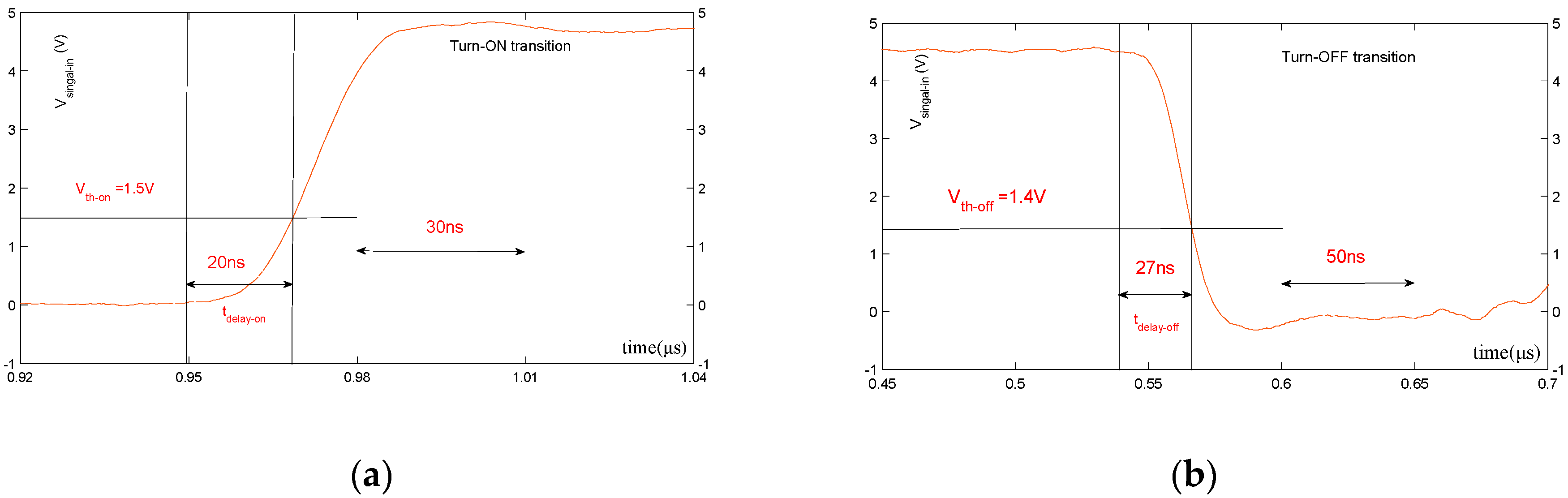
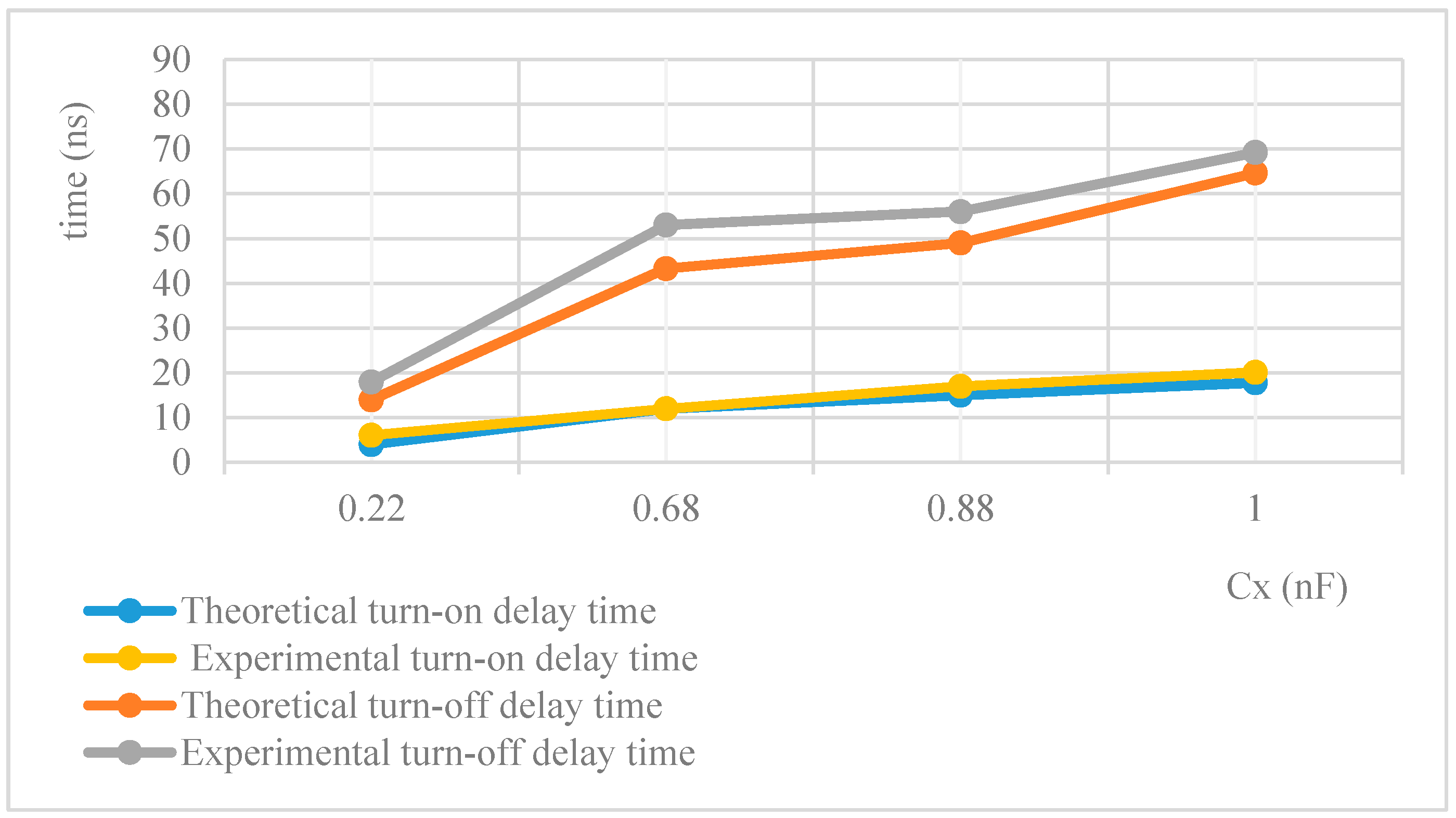
| Parameter | td-on-JFET | td-off-JFET | td-on-driver | td-off-driver | td-on | td-off | VS |
| Value | 53 ns | 60 ns | 50 ns | 42 ns | 20 ns | 27 ns | 5 V |
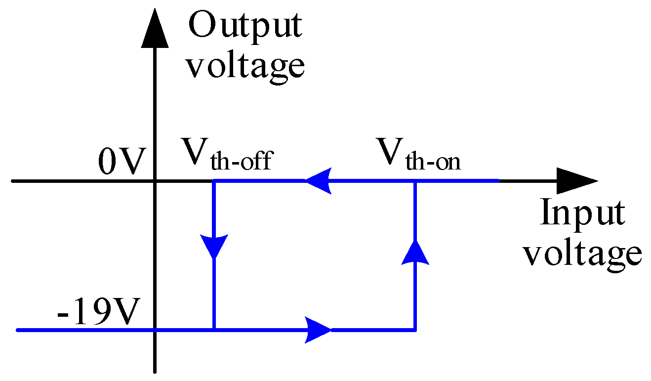
| Parameter | RS | fS | Vth-on | Vth-off | ∂d-on-max | ∂d-off-max | ∂width-change-max |
| Value | 50 Ω 1 | 50 kHz | 1.5 V | 1.4 V | 0.01 | 0.01 | 0.01 |
| Experimental Condition | Maximum Vin without Causing UTO | VDD Settling Time | Overshoot of VDD | iD Settling Time | Overshoot of iD | Turn-Off Loss | Turn-On Loss |
|---|---|---|---|---|---|---|---|
| Without using CX | 103 V | - | - | - | - | - | - |
| CX = 0.22 nF | 227 V | - | - | - | - | - | - |
| CX = 0.68 nF | >550 V 1 | - | - | - | - | - | - |
| Vin = 103 V, IL = 2.0 A, CX = 0.68 nF | - | 1.7 μs | 45% | 1.8μs | 80% | 9.2 μJ | 6.5 μJ |
| Vin = 103 V, IL = 2.0 A, CX = 0.68 nF, CJ = 1.0 nF | - | 1.8 μs | 23% | 1.7 μs | 77% | 8.4 μJ | 6.2 μJ |
| Vin = 103 V, IL = 2.0 A, CX = 0.68 nF | - | 1.7 μs | 45% | 1.8 μs | 80% | 9.2 μJ | 6.5 μJ |
| Vin = 103 V, IL = 2.0 A, CX = 0.68 nF, ferrite ring | - | 1.1 μs | 72% | 1.0 μs | 30% | 11.1 μJ | 4.1 μJ |
| Vin = 303 V, IL = 6.1 A, CX = 0.68 nF | - | 1.1 μs | 64% | 2.3 μs | 72% | 42.3 μJ | 40.1 μJ |
| Vin = 303 V, IL = 6.1 A, CX = 0.68 nF, CJ = 1.0 nF, ferrite ring | - | 1.8 μs | 29% | 1.1 μs | 26% | 48.6 μJ | 18.5 μJ |
© 2018 by the authors. Licensee MDPI, Basel, Switzerland. This article is an open access article distributed under the terms and conditions of the Creative Commons Attribution (CC BY) license (http://creativecommons.org/licenses/by/4.0/).
Share and Cite
Wang, L.; Yang, J.; Ma, H.; Wang, Z.; Olanrewaju, K.O.; Kerrouche, K.D.E. Analysis and Suppression of Unwanted Turn-On and Parasitic Oscillation in SiC JFET-Based Bi-Directional Switches. Electronics 2018, 7, 126. https://doi.org/10.3390/electronics7080126
Wang L, Yang J, Ma H, Wang Z, Olanrewaju KO, Kerrouche KDE. Analysis and Suppression of Unwanted Turn-On and Parasitic Oscillation in SiC JFET-Based Bi-Directional Switches. Electronics. 2018; 7(8):126. https://doi.org/10.3390/electronics7080126
Chicago/Turabian StyleWang, Lina, Junyi Yang, Haobo Ma, Zeyuan Wang, Kabir Oladele Olanrewaju, and Kamel Djamel Eddine Kerrouche. 2018. "Analysis and Suppression of Unwanted Turn-On and Parasitic Oscillation in SiC JFET-Based Bi-Directional Switches" Electronics 7, no. 8: 126. https://doi.org/10.3390/electronics7080126