A Low Hardware Consumption Elliptic Curve Cryptographic Architecture over GF(p) in Embedded Application


1
School of Automation, Guangdong University of Technology, Guangzhou 510006, China
2
Company of Chipeye Microelectronics Foshan Ltd., Foshan 528225, China
*
Authors to whom correspondence should be addressed.
Electronics 2018, 7(7), 104; https://doi.org/10.3390/electronics7070104
Submission received: 11 June 2018
/
Revised: 26 June 2018
/
Accepted: 29 June 2018
/
Published: 3 July 2018
Abstract
:In this paper, a low hardware consumption design of elliptic curve cryptography (ECC) over GF(p) in embedded applications is proposed. The adder-based architecture is explored to reduce the hardware consumption of performing scalar multiplication (SM). The Interleaved Modular Multiplication Algorithm and Binary Modular Inversion Algorithm are improved and implemented with two full-word adder units. The full-word register units for data storage are also optimized. The design is based on two full-word adder units and twelve full-word register units of pipeline structure and was implemented on Xilinx Virtex-4 platform. Design Compiler is used to synthesized the proposed architecture with 0.13 m CMOS standard cell library. For 160, 192, 224, 256 field order, the proposed architecture consumes 5595, 7080, 8423, 9370 slices, respectively, and saves 17.58∼54.93% slice resources on FPGA platform when compared with other design architectures. The synthesized result uses 35.43 k, 43.37 k, 50.38 k, 57.05 k gate area and saves 52.56∼91.34% in terms of gate count in comparison. The design takes 2.56∼4.07 ms to perform SM operation over different field order under 150 MHz frequency. The proposed architecture is safe from simple power analysis (SPA). Thus, it is a good choice for embedded applications.
1. Introduction
Elliptic curve cryptography (ECC) is an asymmetric cryptography proposed in 1986 by Miller [1] and Koblitz [2]. The main advantage of ECC is that it uses a smaller key than some other methods, such as the RSA encryption algorithm, to provide a comparable or higher level of security. International standard organizations, such as NIST [3], ANSI [4] and IEEE [5], have standardized ECC.
Many hardware implementations of ECC have been proposed [6,7,8,9,10,11,12,13,14,15,16,17,18] for ECC. The accelerator of modular multiplication (MM) can be divided into two categories: multiplier-based architecture and adder-based architectures. Multiplier-based architecture includes specific prime field multiplication and Montgomery Multiplication [19]. Adder-based architecture uses Interleaved Multiplication algorithm [20]. Design in [8] is based on modified Montgomery multiplication algorithm using an r-bit × r-bit multiplier. Designs in [9,10] are based on specific prime field and use a full-size n-bit × n-bit multiplier and fast reduction operation to perform MM. However, multiplier-based architecture consumes large hardware area. Modular inversion (MI) operation is another tedious operation in ECC. Binary Modular Inversion Algorithm is well known adder-based MI algorithm. The MM and MI units in design [12] are adder based but two operation units are independent and do not share adder with each other.
In this paper, an adder-based architecture with low hardware consumption over GF(p) is proposed. The main contributions of this paper are as follows:
- Interleaved Modular Multiplication Algorithm and Binary Modular Inversion Algorithm are improved carefully to make full use of hardware source of adder and register. MM and MI are implemented with two full-word adder units and four full-word register units.
- The utilization of registers is optimized to minimize the hardware area. For data register, MA, MS, MM, MI consume four full-word register units and scalar multiplication (SM) operation uses eight full-word register units.
- The architecture is flexible and safe from SPA. The parameters, such as prime value p, elliptic curve point P and scalar value k, can be easily deployed without hardware reconfiguration.
The rest of the paper is arranged as follows. Section 2 reviews the elliptic curve (EC) and EC scalar multiplication (SM). Section 3 presents a low hardware consumption architecture over GF(p). Section 4 gives the result of the implement followed by analysis and comparison with other designs. The paper is concluded in Section 5.
2. Mathematical Background
2.1. Elliptic Curve Over GF(p)
This section provides a brief introduction to elliptic curve over GF(p) and the finite field arithmetic involved. More information about elliptic curve cryptographic primitives can be found in [5,21]. A non-super singular elliptic curve E over GF(p) for p > 3 can be described by Weierstrass equation.
where x, y, a and b are elements of GF(p) and (mod p). The set of points () which satisfies Weierstrass equations together with the point at infinity consists an abelian group.
In affine coordinates, the point addition (PA) and point doubling (PD) operations can be represented as follows: assuming that and are on the elliptic curve, PA formulas for computing are:
with
When , i.e., adding a point to itself, this special case operation is called PD operation. In this paper, only two full-word adder units are needed. In affine coordination, PA operation consists of one MI, two MM, and six MA/MS operations, whereas PD operation needs one MM and two MA/MS more operations than PA. In order to reduce the power dissipation, optimization of MM and MI operation are significant on the overall performance of the SM operation.
2.2. Elliptic Curve Scalar Multiplication
Scalar multiplication (SM) operation is an elemental operation of elliptic curve crypto systems. The scalar multiplication is an operation of adding a EC point P to itself k times, denoted , where , l is the binary length of k. The scalar multiplication algorithm needs to be able to resist simple power analysis (SPA) attacks. Therefore it is necessary to perform scalar multiplication as described in Algorithm 1 bellow, where PA and PD operations are performed for every bit of the scalar.
| Algorithm 1: Elliptic Curve SPA Resistant Scalar Multiplication |
| Input: scalar k and, EC point P Output: EC point : 1: ; 2: for down to 0 do 3: 4: 5: 6: end 7: reture |
3. Scalar Multiplication Architecture
In this section, a bottom-up optimization algorithm over GF(p) is presented, which takes advantage of maximum reuse of adder unit.
3.1. Modular Addition/Subtraction
Modular addition (MA) and modular subtraction (MS) operations are performed as two step operations of addition and subtraction operations according to Algorithm 2 given bellow. The most significant bit of subtraction result can be used as the result of comparing the two numbers, for example in MA operation, where n is the length of p. In FPGA or ASIC, we could achieve addition or subtraction operation with almost equal hardware, that is to say same adder. In proposed design, MA and MS operations are performed in one cycle, so need two full-word adders. The adder is considered as the minimum unit.
| Algorithm 2: Modular Addition and Subtraction in GF(p) | |
| Input: : is prime field. | Input: : is prime field. |
| Output: R: | Output: R: |
| 1: | 1: |
| 2: | 2: |
| 3: if then | 3: if then |
| 4: return | 4: return |
| 5: else | 5: else |
| 6: return | 6: return |
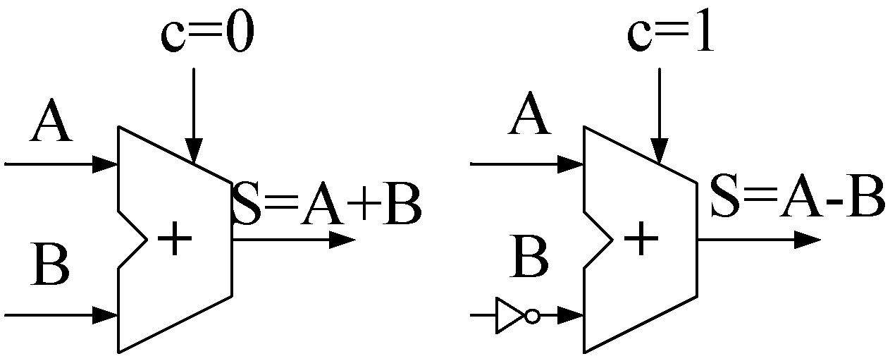
The architecture of two used full-word adder units are illustrated in Figure 1. Left diagram is the minimum adder unit, which can easily be modified to perform subtraction using B’s complement and as shown in right.
3.2. Modular Multiplication
Modular multiplication (MM) operation is an important component in the implementation of SM operation. Traditional high-speed MM implementations use Montgomery multiplication or specific prime field modular multiplication. In affine coordination, we choose Standard Interleaved Modular Multiplication shown in Algorithm 3 given bellow. This algorithm has some disadvantages: (1) The algorithm needs three additions with carry propagation in step 3 to step 5; (2) The comparison in step 4 and 5 requires check of the all lengths of the operands in the worst case. The carry propagation of addition has a significant influence on the latency. Before addition, the comparison must be performed for MSB first. Those two operations cannot be pipelined without delay. There are researchers have tried to address these problems previously, such as shown in [22]. In which, Algorithm 4 adopts Modular multiplication using carry save addition and Algorithm 5 uses Optimized version of the new algorithm. Algorithm 4 uses carry save adders to perform the additions inside the loop, and Algorithm 5 uses lookup-table to reduce both area and time. Both algorithms have high complexity and are unsuitable for the proposed design in this paper.
An improved Interleaved Modular Multiplication Algorithm is given in Algorithm 4 given bellow. The step 4 in Algorithm 4 are used to replace the step 4 and step 5 in Algorithm 3 given bellow. This modification addresses the timing latency of comparison and uses only two adders in one iteration. After step 5 in Algorithm 3, because R may be greater than , the computation of (R mod p) needs two clock cycles with one full-word adder. In step 4 of Algorithm 4, is computed instead of , resulting one cycle saving in every iteration compared with Algorithm 3. is the two most significant bit of R and its value is 0∼3.
| Algorithm 3: Standard Interleaved Modular Multiplication Algorithm |
| Input: : is prime field. Output: R: 1: 2: for downto 0 do 3: 4: if then 5: if then 6: end 7: return R |
| Algorithm 4: Interleaved Modular Multiplication Algorithm |
| Input: : is prime field. Output: R: 1: 2: for downto 0 do 3: 4: 5: end 6: if then 7: return R |
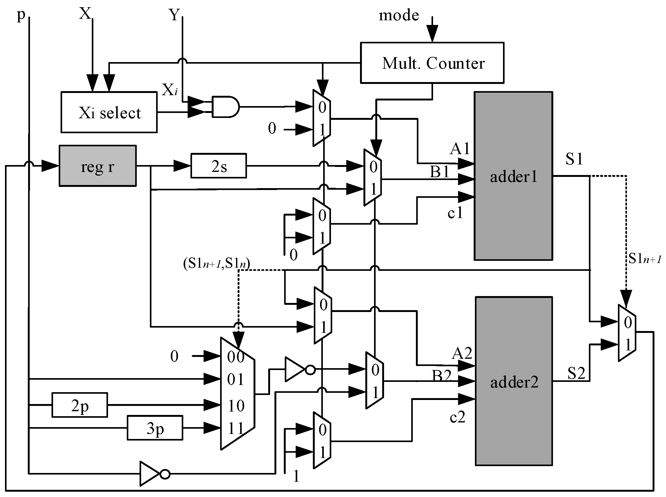
The algorithm is implemented using the architecture shown in Figure 2. The implementation uses only two full-word adder units shown in Figure 1 and one full-word register unit. For simplicity, Figure 2 omits the output data and modular switch multiplexors which select input data to adders for MA, MS, MM and MI. The Mult. Counter block, which is a down iteration counter, creates control signal for selecting the i-th bit of X and selection signal for Mux before adders. When the counter’s number reduced to 0, the iteration finishes. In Algorithm 4 given above, step 3 to 5 was performed in one cycle. Thus, the loop in step 2 to step 5 in Algorithm 4 takes n cycles and MM consumes () cycles, where n is field order. Step 6 is required to make sure the result .
3.3. Modular Inversion
Modular inversion (MI) operation is another significant component in the implementation of SM operation. In order to using the same adder units shown in Figure 1, Binary Modular Inversion Algorithm presented in [23] is selected. By assigning a instead of 1 to variable s in step 1 of Algorithm 5 given bellow, the result y satisfies . This way, both MI and MM operations can be achieved in the same run time. To guarantee all operations of each step finish in one cycle, one comparator and three adders are needed in step 4. The comparator is needed for comparison of u and v. Two adders are used for modular subtraction and one adder is required for subtraction .
| Algorithm 5: Binary Modular Inversion Algorithm |
| Input: Output: y, satisfying step1: ; ; ; ; step2: if (u is even) ; if (r is odd) ; else if (r is negative) ; else ; step3: if (v is even) ; if (s is odd) else if (s is negative) else step4: if (both u and v are odd) if () ; ; else ; ; step5: if () if () return ; else return r. else if () if () return ; else return s. else go to step 2. |
Algorithm 5 given above is the modified version of Binary Modular Inversion Algorithm to achieve minimum hardware consumption. In step 4, the comparison result of u and v can be pre-calculated in step 2 or step 3 and this step completes only the calculation of and or and . In the case of r is negative in step 4, can be calculated by adding r to p and right shifting in step 2 when r is positive odd or negative odd. Similar cases are handled the same way.
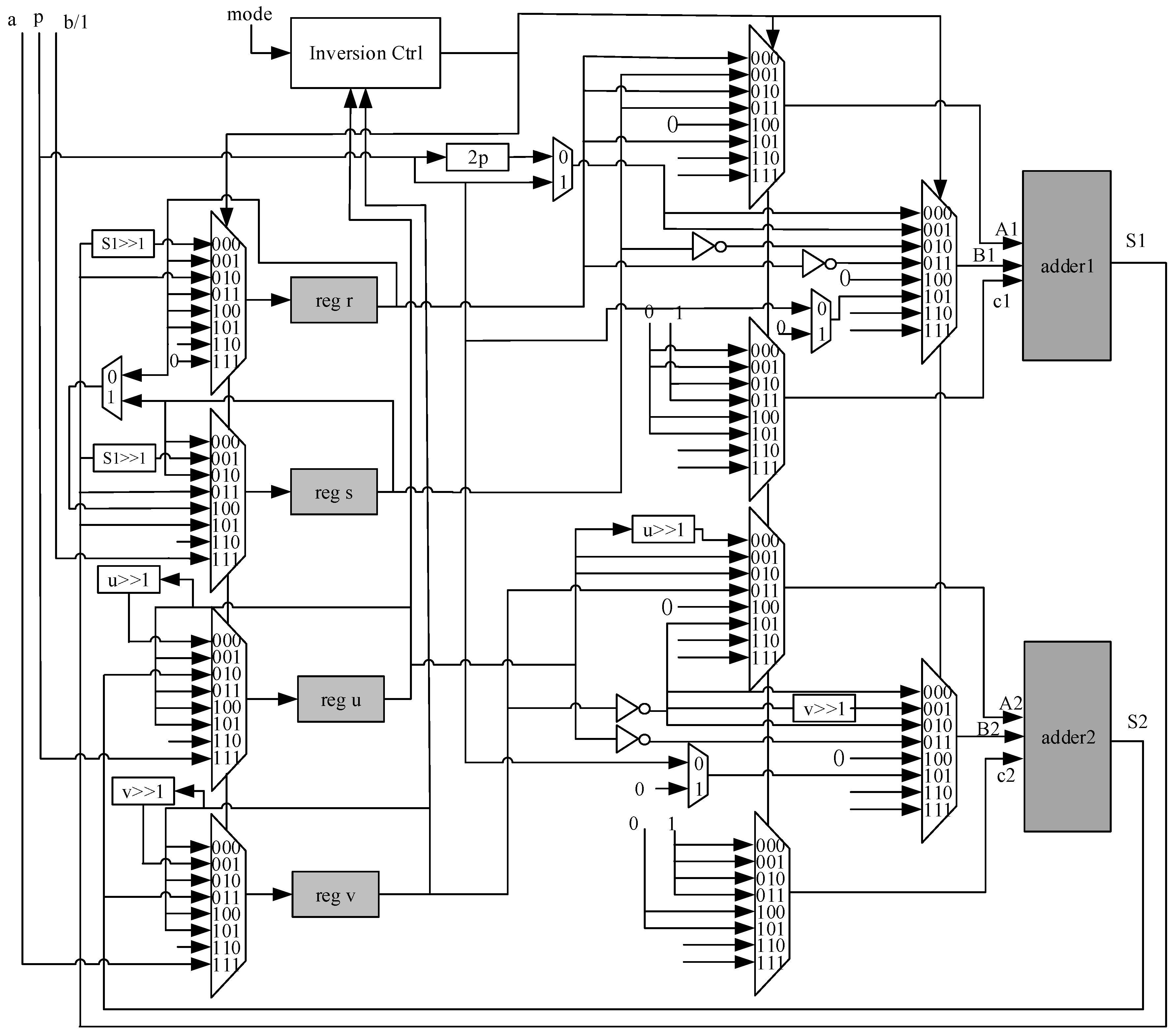
Figure 3 bellow gives the design architecture of implementing Algorithm 5. For simplicity, the output data and modular switch multiplexors, which select input data of adders for MA, MS, MM and MI, are omitted in Figure 3. The Inversion Ctrl block is a state machine of seven state: for step 1, for setp 2, for step 3, and for step 4, for step 5 and for finish. Table 1 bellow shows the data and operators of each step in Algorithm 5. In step 2 or step 3, with the exception of performing or , or should be executed in order to pre-calculate comparison result of u and v for step 4.
At each iteration in step 2 and 3, either u or v is reduced one bit of length, and total number of iterations is , where n is field order. In worst case, the number of iterations of step 4 is . Therefore, the overall total number of iterations is at most .
3.4. Point Addition and Point Doubling
The MA, MS, MM, MI operations have been introduced above. Because all those operations use the same adder units and the same register units, the operations must be performed one after one. Point addition (PA) and point doubling (PD) operations consist of those operations. The scheduling of those operations in PA and PD of proposed architecture is given by Algorithm 6 bellow. It is noted that PA and PD operations need six full-word registers: . The remaining two registers are used for SM scalar k and prime field p.
| Algorithm 6: Point Addition and Point Doubling | |
| Input: ), | Input: , |
| Output: | where and |
| 1: | Output: |
| 2: | 1: |
| 3: | 2: |
| 4: | 3: |
| 5: | 4: |
| 6: | 5: |
| 7: | 6: |
| 8: | 7: |
| 9: | 8: |
| 10: return , | 9: |
| 10: | |
| 11: | |
| 12: | |
| 13: return , | |
3.5. Scalar Multiplier Architecture
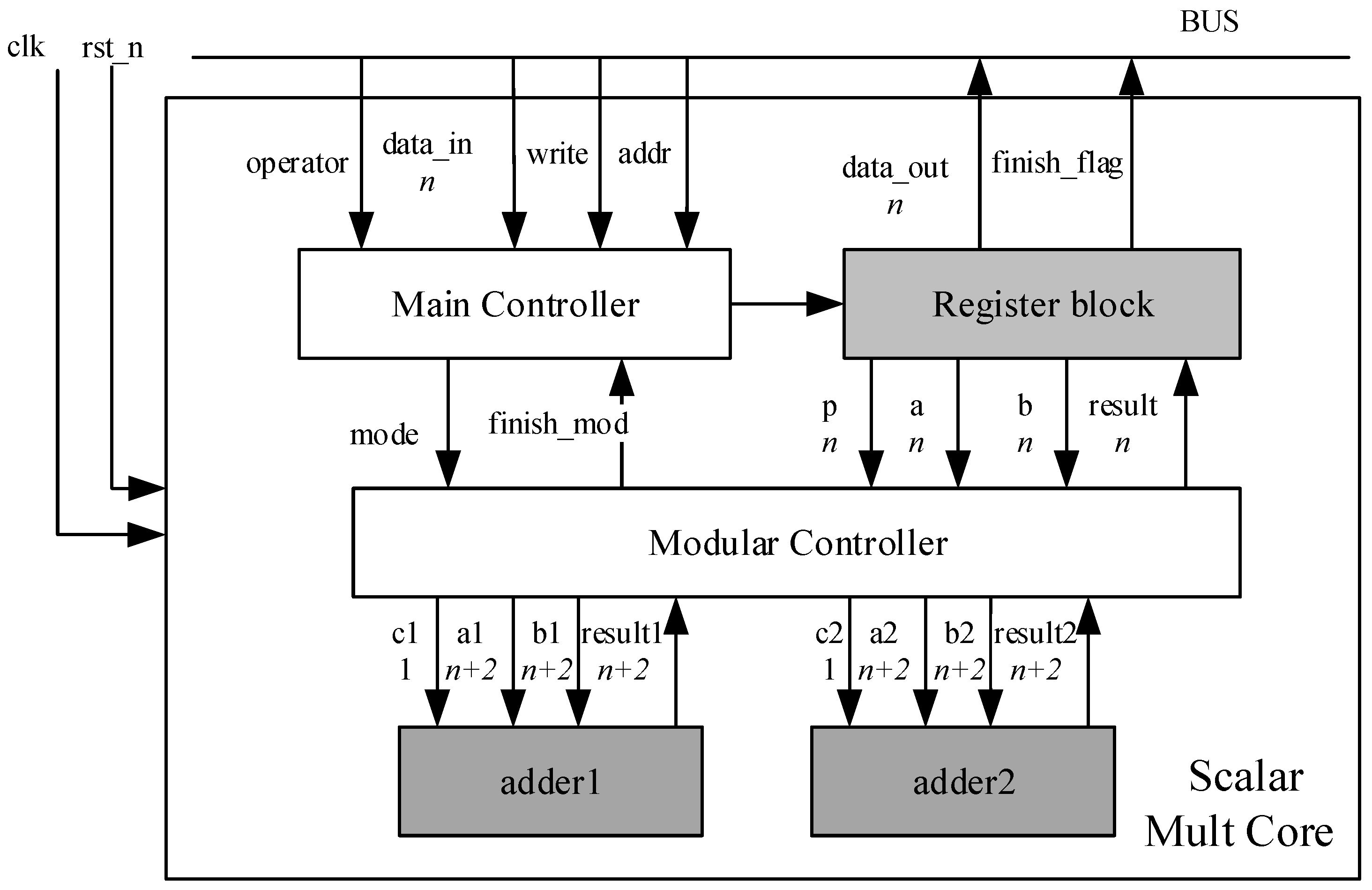
In this section, the block diagram of scalar multiplication over GF(p) is given in Figure 4.
Scalar Mult Core block performs modular operations, MA, MS, MI, MM, and point operations, PA, PD, SM. The finish-flag signal is set to high when all the calculations are done and the result is ready for master system.
Main Controller block is a state machine which controls PA, PD and SM operations. In addition, it also controls data transforming from Register Block to Modular Controller and from Modular Controller to Register Block.
Modular Controller block performs one of MA, MS, MM, and MI operations at a time.
4. Implementation and Result
The elliptic curve scalar multiplication architecture described above was implemented using Verilog-HDL language. The design was synthesized using Design Compiler with the 130-nm CMOS standard cell library. The hardware area is evaluated based on a 2-way NAND gate. This architecture is also implemented on FPGA platform Xilinx Virtex-4 xc4vsx35, using Modelsim for simulation and Xilinx ISE 14.7 for synthesis, mapping, and routing.
Since MI operation can also perform the computation , PA operation needs 1 MI, 2 MMs and 6 MA/MSs and PD operation needs 1 MI, 3 MMs and 8 MA/MSs in Algorithm 6 given above. The number of cycles for the PA and PD operations are given by (4), respectively.
where I is the cycles of MI operation, M is the cycles of MM operation and A is the cycles of MA/MS operation. The total number of cycles to perform SM operation is given by (5).
where n is prime field order.
Table 2 shows the execution cycles of different operations over 160∼256 field order. In 100 tests, a 256-bit EC takes 1066 cycles for PA operation, 1325 cycles for PD operation and 610 k cycles for SM operation.
The proposed architecture costs two full-word adder units and twelve full-word register units. Table 3 shows that the hardware consumption of all registers and adders occupied 42% of total area in average. Register includes twelve register units for data storage and other non-combination. As the bit width increases, the hardware consumption percent of the adder units increased from 13.72% to 15.09%.
The inversion and multiplier units in [12] are implemented by using the Binary Inversion Algorithm and Interleaved Modular Multiplication Algorithm, similar to this work. However, the design in [12] uses two inversions and two multipliers whereas the proposed design here uses one inversion and one multiplier, both based same two adder units. As shown in Table 4, in 256-bit field order, the design in [12] requires 167.5 k gate while this design uses 57.05 k gate, saving 65.94% hardware resource. In the given field order, AT parameter of this design is 232 and the AT of [12] is 504. This design has advantages of area-time product. The proposed design saves 64.77% to 65.94% hardware resource comparing with [12] under different field order.
The design in [8] adopts word-based Montgomery multiplier with an optimized data bus and an on-the-fly redundant binary converter boost the throughput of the EC scalar multiplication. Compared with [8] in different field order, the proposed design saves 52.56∼69.85% hardware resource. The design in [10] is based on full-size 256-bit × 256-bit multiplier and uses 659 k gates to implement. The design in [15] is based on systolic arithmetic unit and operates in higher frequency at 556 MHz. The designs in [10,15] has smaller AT parameters than the proposed design here.Compared whit designs in [8,10,12,15], the proposed design here consumes least hardware, saving 52.56∼91.34% hardware resource on the average.
The processor in [16] consists of with CPU, data RAM, program memory and others. Though it consumes 11.686 k gate area, but it perform one scalar multiplication operation requires up to 1003 k clock cycles, 2.93 times over this proposed design here. The scalar multiplication execution time and energy of [16] can be computed from cycles, frequency and power. The total energy to perform one 192-bit scalar multiplication of this proposed design is 18.65 J while the processor in [16] is 114.20 J. Because the low frequency with 1.695 MHz, the processor in [16] has very large scalar multiplication execution time with 592 ms. The processor in [17] consumes five m-bit registers and require seven multiply operations per key bit in GF(). It has little area and energy than this proposed design here. However, it did not give detail information about scalar multiplication execution time or frequency, so there is no way to compare the SM operation time with the proposed design here. The design in [18] adopts registers and bit-level multiplier share method and consumes 11.571 k gates area. The complexity of the scalar multiplication between GF(p) and GF() is different, as example, the modular addition needs carry addition and modulo p operation in GF(p) while modular addition needs just xor operation in GF(). The modular addition is fundamental operation in low area ECC architecture. Therefore is difficult to compare which are better among [17,18] and the proposed design here from area consumption and operation time.
Table 5 provides detailed data of the proposed hardware implement of EC designs over 160, 192, 224, 256 field order on given FGPA platform. It consumes 239, 342, 468, 610 clock cycles and takes 5595, 7080, 8423, 9370 Slices to perform SM operation. The SM operation costs 239 clock cycles with 9199 Slice LUTs, 2833 Flip Flops and 8 DPS48s in 160 field order.
Table 6 shows the performance data of several existing FPGA implementations based on EC scalar multiplication. The architecture in [6] is based on a unified Add/Sub/Mul unit. It consumes 13,158 Slices over 256 field order while architecture designed in this paper consumes 9370 Slices. On the same platform, the proposed architecture saves 17.58∼28.79% on average in terms of used slices comparing with [6] over different field orders. The architectures proposed in [6,12] are capable of resisting SPA. The architectures in [13,14] are designed to implement Elliptic Curve Digital Signature Algorithm over GF() while the scalar multiplication implementation data are given in the above Table 6. Compared with [13] over 163 field order, architecture provided in this paper uses 42.14% less slices over 160 field order and 26.78% less slices over 192 field order. The proposed architecture has the lowest hardware consumption among designs given in above Table 6.
5. Conclusions
In this paper, a low hardware consumption and SPA resistant elliptic curve design over GF(p) is presented. Using two full-word adder units, a bottom-up optimization approach is developed to schedule all operations of scalar multiplication at algorithm level. The Interleaved Modular Multiplication Algorithm and Binary Modular Inversion Algorithm are improved to make them implementable using two adder units. The utilization of registers is also optimized and uses only twelve full-word register units for data storage in the design implementation. The proposed architecture has been synthesized by Xilinx ISE14.7 on a Virtex-4 platform and Design Compiler using 130 nm CMOS. Compared with other designs, it uses 17.58∼54.93% fewer slices on the FGPA platform and 52.56∼91.34% fewer gates in ASIC over 160, 192, 224, 256 field orders. The architecture is reconfigurable for any prime p and is also safe from simple power analysis attracts. It suites ECC in embedded applications.
Author Contributions
X.H. and S.Z. provided the idea, performed the experiments and managed the paper. X.Z., S.C. and X.X. assisted in idea development and paper writing.
Funding
This work is supported by Science and Technology Planning Project of Guangdong Province of China (2015B010128013, 2015B090911001 and 2015B090912001).
Conflicts of Interest
The authors declare no conflict of interest.
Abbreviations
The following abbreviations are used in this manuscript:
| ECC | elliptic curve cryptography |
| EC | elliptic curve |
| SM | scalar multiplication |
| MM | modular multiplication |
| MI | modular inversion |
| MA | modular addition |
| MS | modular subtraction |
| PA | point addition |
| PD | point doubling |
References
- Miller, V.S. Use of elliptic curves in cryptography. In Proceedings of the Annual International Cryptology Conference (CRYPTO), Santa Barbara, CA, USA, 18–22 August 1985; pp. 417–426. [Google Scholar]
- Koblitz, N. Elliptic curve cryptosystems. Math. Comput. 1987, 48, 203–209. [Google Scholar] [CrossRef]
- National Institute of Standards and Technology. Digital Signature Standard; FIPS Publication 186-2; National Institute of Standards and Technology: Gaithersburg, MD, USA, 2000.
- American National Standards Institute. ANSI X9.63, Public Key Cryptography for the Financial Services Industry: Elliptic Curve Key Agreement and Key Transport Protocols; American National Standards Institute: Washington, DC, USA, 2000. [Google Scholar]
- Institute of Electrical and Electronic Engineers. P1363 Standard Specifications for Public Key Cryptography; Institute of Electrical and Electronic Engineers: Piscataway, NJ, USA, 2000. [Google Scholar]
- Javeed, K.; Wang, X. FPGA Based High Speed SPA Resistant Elliptic Curve Scalar Multiplier Architecture. Int. J. Reconfig. Comput. 2016, 2016, 6371403. [Google Scholar] [CrossRef]
- Marzouqi, H.; Al-Qutayri, M.; Salah, K. Review of Elliptic Curve Cryptography processor designs. Microprocess. Microsyst. 2015, 39, 97–112. [Google Scholar] [CrossRef]
- Satoh, A.; Takano, K. A scalable dual-field elliptic curve cryptographic processor. IEEE Trans. Comput. 2003, 52, 449–460. [Google Scholar] [CrossRef]
- Paar, C. Ultra High Performance ECC over NIST Primes on Commercial FPGAs. In Proceedings of the International Workshop on Cryptographic Hardware and Embedded Systems, Washington, DC, USA, 10–13 August 2008; Springer: Berlin/Heidelberg, Germany, 2008; pp. 62–78. [Google Scholar]
- Zhao, Z.; Bai, G. Ultra High-Speed SM2 ASIC Implementation. In Proceedings of the 2014 IEEE 13th International Conference on Trust, Security and Privacy in Computing and Communications, Beijing, China, 24–26 September 2014; pp. 182–188. [Google Scholar]
- Khan, Z.-U.-A.; Benaissa, M. Throughput/Area-efficient ECC Processor Using Montgomery Point Multiplication on FPGA. IEEE Trans. Circuits Syst. II Express Briefs 2015, 62, 1078–1082. [Google Scholar] [CrossRef]
- Ghosh, S.; Alam, M.; Chowdhury, D.R.; Gupta, I.S. Parallel crypto-devices for GF(p) elliptic curve multiplication resistant against side channel attacks. Comput. Electr. Eng. 2009, 35, 329–338. [Google Scholar] [CrossRef]
- Sghaier, A.; Zeghid, M.; Massoud, C.; Mahchout, M. Design And Implementation of Low Area/Power Elliptic Curve Digital Signature Hardware Core. Electronics 2017, 6, 46. [Google Scholar] [CrossRef]
- Wajih, E.; Noura, B.; Mohsen, M.; Rached, T. Low Power Elliptic Curve Digital Signature Design for Constrained Devices. Int. J. Secur. 2012, 6, 1–14. [Google Scholar]
- Chen, G.; Bai, G.; Chen, H. A High-Performance elliptic curve cryptographic processor for general curves over GF(p) based on a systolic arithmetic unit. IEEE Trans. Circuits Syst. II Express Briefs 2007, 54, 412–416. [Google Scholar] [CrossRef]
- Wenger, E.; Feldhofer, M.; Felber, N. Low-resource hardware design of an elliptic curve processor for contactless devices. In Proceedings of the International Conference on Information Security Applications, Jeju Island, Korea, 24–26 August 2010; Springer: Berlin/Heidelberg, Germany, 2010; pp. 92–106. [Google Scholar]
- Leinweber, L.; Papachristou, C.; Wolff, F.G. Efficient architectures for elliptic curve cryptography processors for RFID. In Proceedings of the IEEE International Conference on Computer Design, Lake Tahoe, CA, USA, 4–7 October 2009; pp. 372–377. [Google Scholar]
- Azarderakhsh, R.; Järvinen, K.U.; Mozaffari-Kermani, M. Efficient algorithm and architecture for elliptic curve cryptography for extremely constrained secure applications. IEEE Trans. Circuits Syst. I Regul. Pap. 2014, 61, 1144–1155. [Google Scholar] [CrossRef]
- Montgomery, P.L. Modular multiplication without trial division. Math. Comput. 1985, 44, 519–521. [Google Scholar] [CrossRef]
- Nassar, M.A.; El-Sayed, L.A.A. Efficient interleaved modular multiplication based on sign detection. In Proceedings of the 2015 IEEE/ACS 12th International Conference of Computer Systems and Applications (AICCSA), Marrakech, Morocco, 17–20 November 2015; pp. 1–5. [Google Scholar]
- Hankerson, D.; Menezes, A.; Vanstone, S. Guide to Elliptic Curve Cryptography; Springer: New York, NY, USA, 2004. [Google Scholar]
- Amanor, D.N.; Paar, C.; Pelzl, J.; Bunimov, V. Efficient Hardware Architectures for Modular Multiplication. Master’s Thesis, The University of Applied Sciences Offenburg, Offenburg, Germany, 2005. [Google Scholar]
- Ghosh, S.; Alam, M.; Gupta, I.S.; Chowdhury, D.R. A Robust GF(p) parallel arithmetic unit for public key cryptography. In Proceedings of the 10th Euromicro Conference on Digital System Design Architectures, Methods and Tools (DSD 2007), Lubeak, Germany, 29–31 August 2007; pp. 109–115. [Google Scholar]
- Urbano-Molano, F.A.; Trujillo-Olaya, V.; Velasco-Medina, J. Design of an elliptic curve cryptoprocessor using optimal normal basis over GF(2233). In Proceedings of the 2013 IEEE 4th Latin American Symposium on Circuits and Systems (LASCAS), Cusco, Peru, 27 February–1 March 2013; pp. 1–4. [Google Scholar]
Figure 1.
Adder unit.

Figure 2.
Multiplication diagram.

Figure 3.
Inversion diagram.

Figure 4.
Inversion diagram.


Table 1.
Inversion state and Mux.
| State | 111 | 000 | 001 | 010 | 011 | 100 | 101 | 110 |
|---|---|---|---|---|---|---|---|---|
| + | + | − | − | 0 | + | null | ||
| r | s | r | s | 0 | r | null | ||
| 0 | null | |||||||
| 0 | 0 | 1 | 1 | 0 | 0 | null | ||
| − | − | − | − | 0 | + | null | ||
| u | u | v | 0 | s | null | |||
| 0 | null | |||||||
| 1 | 1 | 1 | 1 | 0 | 0 | null | ||
| r | 0 | r | r | r | r | null | ||
| s | b | s | s | null | ||||
| u | p | u | u | u | u | null | ||
| v | a | v | v | v | v | null |
Table 2.
Execution cycles for different operations.
| Field Order | Number of Cycles | ||||
|---|---|---|---|---|---|
| Modular Mult. | Modular Inversion | Point Addition | Point Doubling | Scalar Mult. | |
| 160 | 163 | 338 | 671 | 834 | 239 k |
| 192 | 195 | 405 | 801 | 998 | 344 k |
| 224 | 227 | 473 | 932 | 1163 | 467 k |
| 256 | 259 | 545 | 1066 | 1325 | 610 k |
Table 3.
Hardware consumption of register and adder on ASIC.
| Field Order | Total Area | Area | Percent | ||||
|---|---|---|---|---|---|---|---|
| Register | Adder | Reg and Add | Register | Adder | Reg and Add | ||
| 160 | 35.43 | 9.91 | 4.86 | 14.77 | 27.97% | 13.72% | 41.69% |
| 192 | 43.37 | 11.83 | 6.26 | 18.09 | 27.28% | 14.43% | 41.71% |
| 224 | 50.38 | 13.93 | 7.23 | 21.16 | 27.65% | 14.35% | 42.00% |
| 256 | 57.05 | 15.75 | 8.61 | 24.36 | 27.61% | 15.09% | 42.70% |
Table 4.
ECC Hardware Performance Comparison on ASIC.
| Design | Technology | Field Order | Area (k gate) | Frequency (MHz) | Cycles (k) | SM (ms) | AT | Power (mW) | Energy (J) |
|---|---|---|---|---|---|---|---|---|---|
| This work | 130 nm | 160 | 35.43 | 150 | 239 | 1.60 | 57 | 7.40 | 11.79 |
| 192 | 43.37 | 150 | 342 | 2.28 | 99 | 8.18 | 18.65 | ||
| 224 | 50.38 | 150 | 468 | 3.12 | 157 | 10.05 | 31.36 | ||
| 256 | 57.05 | 150 | 610 | 4.07 | 232 | 11.60 | 47.17 | ||
| [12] | 130 nm | 160 | 101.3 | 150 | 129.3 | 0.87 | 88 | - | - |
| 192 | 123.1 | 138 | - | 1.36 | 167 | - | - | ||
| 224 | 143.9 | 130 | - | 1.95 | 281 | - | - | ||
| 256 | 167.5 | 110 | - | 3.01 | 504 | - | - | ||
| [8] | 130 nm | 160 | 117.5 | 137.7 | 153 | 1.21 | 142 | - | - |
| 192 | 118.02 | 137.7 | 184 | 1.44 | 170 | - | - | ||
| 224 | 120.26 | 137.7 | 297 | 2.34 | 281 | - | - | ||
| 256 | 120.26 | 137.7 | 340 | 2.68 | 322 | - | - | ||
| [10] | 130 nm | 256 | 659 | 163.7 | 3.3 | 0.02 | 13 | - | - |
| [15] | 130 nm | 256 | 122 | 556 | 562 | 1.01 | 123 | - | - |
| [16] | UMC L180 | P-192 | 11.686 | 1.695 | 1003 | 592 | 6915 | 0.193 | 114.2 |
| [17] | IBM 130 nm | GF() | 8.756 | - | 191 | - | - | - | 4.19 |
| [18] | 65 nm | GF() | 11.571 | 13.56 | 7.87 | 0.58 | 6.71 | 0.077 | 0.61 |
AT: Area * SM, area-time product. Energy: Total energy of 1 scalar multiplication.
Table 5.
FPGA Implementation Result.
| Field Order | Frequency (MHz) | Cycles (k) | Slice LUTs | Flip Flops | DSP | Slice |
|---|---|---|---|---|---|---|
| 160 | 26.89 | 239 | 9199 | 2833 | 8 | 5595 |
| 192 | 21.55 | 342 | 11,184 | 3377 | 10 | 7080 |
| 224 | 20.87 | 468 | 14,184 | 2787 | 12 | 8423 |
| 256 | 20.44 | 610 | 16,195 | 3194 | 14 | 9370 |
Table 6.
colorredECC Hardware Performance Comparison on FPGA.
| Design | Platform | Field Order | Area | Frequency (MHz) | Cycles (k) | SM (ms) |
|---|---|---|---|---|---|---|
| This work | Virtex-4 | 160 | 5595 Slices | 26.89 | 239 | 8.89 |
| 192 | 7080 Slices | 21.55 | 342 | 15.87 | ||
| 224 | 8423 Slices | 20.87 | 468 | 22.43 | ||
| 256 | 9370 Slices | 20.44 | 610 | 29.84 | ||
| [6] | Virtex-4 | 160 | 7088 Slices | 53 | 74.2 | 1.4 |
| 192 | 8590 Slices | 48 | 110.4 | 2.3 | ||
| 224 | 10,800 Slices | 43 | 150.5 | 3.5 | ||
| 256 | 13,158 Slices | 40 | 200.0 | 5.0 | ||
| [12] | Virtex-4 | 160 | 12,415 Slices | 60 | 132.0 | 2.2 |
| 192 | 14,858 Slices | 53 | 185.5 | 3.5 | ||
| 224 | 17,331 Slices | 47 | 253.8 | 5.4 | ||
| 256 | 20,123 Slices | 43 | 331.1 | 7.7 | ||
| [13] | Virtex-5 | GF() | 9670 Slices | 147.5 | 41.7 | 0.283 |
| [14] | Virtex-4 | GF() | 13,016 Slice LUTs | 194.88 | 109.7 | 0.5621 |
| 6823 Flip Flops | ||||||
| [24] | EP3SL150F1153C | GF() | 8799 ALUT | 276.24 | 447.5 | 1.621 |
| 7143 Registers |
© 2018 by the authors. Licensee MDPI, Basel, Switzerland. This article is an open access article distributed under the terms and conditions of the Creative Commons Attribution (CC BY) license (http://creativecommons.org/licenses/by/4.0/).
Share and Cite
MDPI and ACS Style
Hu, X.; Zheng, X.; Zhang, S.; Cai, S.; Xiong, X. A Low Hardware Consumption Elliptic Curve Cryptographic Architecture over GF(p) in Embedded Application. Electronics 2018, 7, 104. https://doi.org/10.3390/electronics7070104
AMA Style
Hu X, Zheng X, Zhang S, Cai S, Xiong X. A Low Hardware Consumption Elliptic Curve Cryptographic Architecture over GF(p) in Embedded Application. Electronics. 2018; 7(7):104. https://doi.org/10.3390/electronics7070104
Chicago/Turabian StyleHu, Xianghong, Xin Zheng, Shengshi Zhang, Shuting Cai, and Xiaoming Xiong. 2018. "A Low Hardware Consumption Elliptic Curve Cryptographic Architecture over GF(p) in Embedded Application" Electronics 7, no. 7: 104. https://doi.org/10.3390/electronics7070104
Note that from the first issue of 2016, this journal uses article numbers instead of page numbers. See further details here.