Prediction of the Nonlinearity by Segmentation and Matching Precision of a Hybrid R-I Digital-to-Analog Converter


1
Shenzhen Institutes of Advanced Technology, Chinese Academy of Sciences, Shenzhen 518055, China
2
Institute of Microelectronics of Chinese Academy of Sciences, Beijing100029, China
3
University of Chinese Academy of Sciences, Beijing 100049, China
*
Author to whom correspondence should be addressed.
Electronics 2018, 7(6), 91; https://doi.org/10.3390/electronics7060091
Submission received: 20 March 2018
/
Revised: 9 May 2018
/
Accepted: 1 June 2018
/
Published: 6 June 2018
Abstract
:The data converters’ nonlinearity, which is mainly caused by random mismatch, reflects the performance deviation between the actual realization and an ideal situation. The interpretation of the numerical relationship between the nonlinearity and matching precision for a hybrid digital-to-analog converter (DAC) consisting of a k-bit resistor-string and an m-bit current-steering array (R-I DAC) is a challenging task. In this article, we propose a method to predict the nonlinearity by the segmentation and matching-precision of an R-I DAC. First, we propose a mathematical model that focuses on the output and mismatches of an R-I DAC. The model shows that nonlinearity gets worse when the segmentation ratio (k/m) increases. Second, we derive theoretical expressions for the static nonlinearity and matching precision. It is shown that the resolution number of resistor (k) has more influence on nonlinearity than the resolution number of current steering (m). Designers can quickly determine the segmentation strategy and matching precision from the derived equations. Finally, we achieve a nonlinearity that is smaller than half the least significant bit (LSB) when the matching resolution in the bits of the resistors and current sources are k + 4 and m + 2k + 2, respectively. For the verification of the study proposed, three test groups of prototypes with different matching precisions are fabricated and measured. The measured static and dynamic performance of the designed DACs support our proposal expressions.
1. Introduction
The data converters’ nonlinearity, which is mainly caused by random mismatch, reflects the performance deviation between an actual realization and an ideal situation. The data converters’ nonlinearity can be categorized into static nonlinearity and dynamic nonlinearity [1,2,3]. Static nonlinearity includes the differential nonlinearity (DNL) and integrated nonlinearity (INL). Dynamic nonlinearity mainly includes the spurious-free dynamic range (SFDR) and the effective number of bits (ENOB). The static nonlinearity is fundamental, and it sets an upper limit of the dynamic nonlinearity [2]. So, the static nonlinearity is addressed.
Static nonlinearity is mainly caused by mismatches that may be random, systematic, or a combination of both. While systematic mismatches can usually be compensated with layout skills and a choice of circuit architecture and calibration, the random mismatches due to the stochastic nature of physical geometry and doping cannot be avoided [4,5,6]. In such a case, random mismatches are the main cause of static nonlinearity. So, research on the mechanisms of random mismatches’ effects on static nonlinearity has been a focus [4,6,7,8,9,10,11,12].
The static nonlinearity mechanism of traditional segmented cascade digital-to-analog converters (DACs) and two-step analog-to-digital converters (ADCs) have been fully understood [13]. A segmented DAC consists of several segments containing corresponding matching units. The static nonlinearity of a traditional segmented DAC is a linear combination of mismatches of different segments. Specifically, for traditional segmented cascade DACs consisting of two segmented parts, the part with the most significant bits (MSBs) mainly determines the accuracy of the overall converter, and the part with the least significant bits (LSBs) is required for the accuracy of the LSBs as a standalone converter [13]. For example, for an n-bit (m-bit MSBs and k-bit LSBs) traditional segment cascade DAC, the MSBs are required to have n-bit matching accuracy, while the LSBs are required to have k-bit matching accuracy.
A hybrid DAC consisting of a k-bit resistor string and an m-bit current-steering array (R-I DAC) was first proposed in the IEEE international system-on-chip conference (SOCC) 2015 [14]. The R-I DAC is a kind of segmented DAC, using a resistor string as the LSBs part for low-power consumption, and using a current-steering array as the MSBs part for high speed. So, it provides an alternative for medium-speed, low-power applications. Since it adopts an R-I hybrid segmented architecture, its voltage output is generated by multiplying the resistance with the current. The voltage-output linearity is ensured by the matching in resistor units, together with the matching in current source units. Since the output voltage is obtained by the multiplication of the resistance current, the output mismatch is generated by the mismatches of resistors and of current sources. The multiplication itself is a nonlinear operation that makes the accuracy analysis of R-I DAC more difficult than that of traditional segmented DACs. To get the insight of R-I accuracy, this article aims at analyzing the effect of the R-I DAC on the mismatch of the resistors and the current source.
As discussed before, the static nonlinearity of traditional segmented cascade DACs is a linear combination of mismatches of the different segments. In contrast, the static nonlinearity of the R-I DAC is a nonlinear combination of mismatches of the resistor-array segment and the current-array segment. As a result, the nonlinearity performance of the R-I DAC is worse than expected if the matching precision is designed with the conventional segment method [14]. As a practical example, although the accuracy is designed for 1-LSB DNL/INL based on a conventional segment design experience, the measured DNL/INL in Reference [14] is 6.38/7.55 LSB. To solve this problem of worse DNL/INL, this article explores the numerical relationship between nonlinearity and matching precision and segmentation for the R-I DAC, and gives equations to guide parameter design.
The major contributions of this article are summarized as follows. (1) We propose a mathematical model to describe the output of the R-I DAC with segmentation and matching precision. To visualize the nonlinearity mechanism of the R-I DAC, we present an algorithm for Monte Carlo simulation to illustrate the effect of segmentation and matching precision on nonlinearity, which shows that nonlinearity gets worse when the segmentation ratio (k/m) increases. (2) We mathematically derived the expressions of DNL/INL and matching precision. In addition, the mechanism of how the segmentation and matching precision affect dynamic performance is also explored. (3) With the derived equations, designers can quickly determine the segmentation strategy and matching precision. We achieve nonlinearity that is smaller than half the least significant bit (LSB) when the matching resolution in bits of resistors and current sources are k + 4 and m + 2k + 2, respectively. The proposed theory is verified with the measurement results of three test groups with different matching precisions.
The remainder of this paper is organized as follows. Section 2 introduces the architecture of the R-I DAC. Section 3 proposes a mathematical model of the output of the R-I DAC and discusses the variation regularity of the nonlinearity. Section 4 derives the mathematical expression of nonlinearity affected by segmentation and matching precision. Section 5 derives the mathematical expression of the matching precision of a given nonlinearity. Section 6 discusses the dynamic performance. Section 7 designs the prototypes and performs the measurements. Section 8 concludes our work.
2. The Architecture of the R-I Hybrid DAC
Resistor-string digital-to-analog converters (R-DACs) are mostly adopted in low-power, low-speed applications while current-steering DACs (I-DACs) are used in high-power, high-speed applications [2,5,15,16,17,18]. To make a trade-off between speed and power, a resistor-string and current-steering-array hybrid DAC (R-I DAC) was proposed [14].
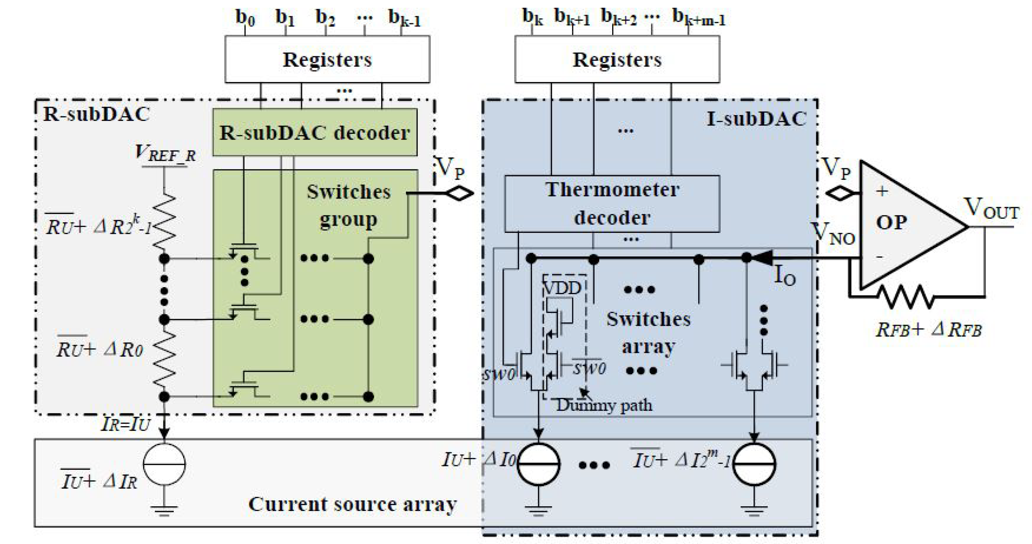
The R-I DAC hybrid architecture is a form of segment technique. An n-bit R-I hybrid DAC is implemented using an m-bit current-steering sub-DAC (I-subDAC) as the most significant bits (MSBs), and a k-bit resistor-string sub-DAC (R-subDAC) as the least significant bits (LSBs). An output operational amplifier (OP) combines MSBs and LSBs. The OP is used in the summer amplifier, which is configured to generate the output voltage. The architecture of the k + m bit resistor-string and current-steering-array hybrid DAC (R-I DAC) with the mismatches between the resistors and currents shown in Figure 1. The mismatch variation of each unit element of the R-subDAC and I-subDAC is modeled as normally distributed random variables, ΔR and ΔI respectively, with a relative variance δ2 and ξ2.
The R-subDAC uses uniform resistors in the series to produce linear node voltages, where VREF-R is the reference voltage. The linear node voltages are connected to the output node VP by the multiplexer. The multiplexer consists of the R-subDAC decoder and its switches group. There are three most common types of resistor string multiplexer architecture: two-dimensional address architecture, full decode architecture, and tree decode architecture [19]. They are different in decoder logic complexity, multiplexer resistance, and junction capacitances. The resolution number is a major consideration to select multiplexer schemes. The resolution number of R-subDAC in Reference [14] is six, and the two-dimensional address architecture is adopted. The R-subDAC resolution number of the prototypes in this article is four, and the tree decode architecture is adopted. The current IR through the resistor string is provided by the matching current source array. The output node VP of R-subDAC connects to the positive input of the output amplifier.
The I-subDAC adopts a glitchless scheme, which is the unary selection with a thermometer decoder [2]. Since the I-subDAC forms MSBs, which have greater weight than LSBs, the glitches generated by the MSBs affect the output more seriously. Since unary selection has less glitch distortion, as well as better DNL and INL than other architectures such as binary structure or segmentation [2], unary selection with a thermometer decoder is adopted. The unit of the current source array is implemented by a sooch cascode current mirror to increase the equivalent resistance and reduce the overdrive voltage [2]. In the I-subDAC, dummy paths are used to keep the unity current generators in the saturation region. As a result, the output signal maintains a high response speed and low noise.
The output amplifier OP adopts a two-stage scheme: a folded cascode input stage and a class-AB output stage to achieve a large open-loop gain A0 [13]. The larger open-loop gain A0 is crucial for the precision of the R-I DAC output voltage. This is because the OP is used in a summer configuration, basing it on the feedback principle. Due to feedback theory, the actual output is (VP + IO × RFB) × A0/(1 + A0) [13]. So, the error between the actual and ideal output voltage VOUT is 1/(1 + A0) × VOUT. The error voltage is required to be less than 1 LSB, so the A0 is required to be greater than 2n, that is, greater than 60.2 dB for a 10-bit DAC. The OP in this article achieves a gain of 83 dB, which is enough for a 13-bit resolution. For a 10-bit R-I DAC, the open-loop gain of the OP in this article is large enough. So, the remaining discussions ignore the error voltage and use the ideal expression for the output voltage.
Assuming the open-loop gain of OP is large enough, Equation (1) is the output expression of the k + m bits R-I DAC, where IU, IR, RFB, and RU are the unity current of the current source array, the current through the resistor string, feedback resistance, and the unit resistance of the resistor string, respectively. They are designed as IU·RFB = 2k·IR·RU, IU = IR, RFB = 2k·RU, n = m + k. The bx represents one bit of the digital input code, where a higher x indicates the more significant value of the bit.
A (6 + 6)-bit R-I DAC prototype was implemented in Reference [14]. To find the reasons for the worse DNL/INL than measured one in Reference [14], we started with numeric simulations for the nonlinearity of the R-I DAC. The following simulations and analysis contain some variables which are summarized in the appendix as variable notations.
3. Variation Regularity of the Nonlinearity Affected by Segmentation and Matching Precision of the R-I DAC
The R-I DAC consists of an R-subDAC and an I-subDAC. To connect them together, two pairs of matching elements are designed. One pair is IU and IR; and the other is RFB and RU, as shown in Figure 1. It is vital to find out the variation regularity of the nonlinearity affected by the segment ratio and matching precision of the R-I DAC.
The variation of each unit of the R-subDAC and I-subDAC are modeled as independent normal random variables, ΔR and ΔI, with a zero expected value and a relative variance δ2 and ξ2, respectively. The unit values IU (RU) are represented by the mismatch value ΔIi (ΔRi) and the expected value (), as shown in Equation (2)
The controlling codes for the R-subDAC and I-subDAC are represented by BL and BH for a digital input with a decimal value of i, respectively, as shown in Equation (3). In Equation (3), B = floor(A) rounds the elements of A to the nearest integers that are less than or equal to A. M = mod (X, Y) returns the modulus after the division of X by Y.
By using Equations (2) and (3), Equation (1) can be re-written as Equation (4)
The physical implications of the mismatching components in Equation (4) are explained as follows. The ξj is a random relative mismatch of a current source unit in the current-steering array, so the component represents the accumulated nonlinearity in the I-subDAC. The δf is a random relative mismatch of a resistor unit in the feedback resistor, so the component represents the accumulated nonlinearity in the feedback resistor, which consists of 2k RU. The ξR is a random relative mismatch of the current source unit biasing the R-subDAC, so BL∙ξR represents the variation of current that flows through the resistor string. The δj is a random relative mismatch of a resistor unit in the resistor divider, so the component represents the accumulated nonlinearity in the R-subDAC. With the expression of nonlinear output in Equation (4), the differential nonlinearity (DNL) and integrated nonlinearity (INL) can be expressed mathematically.
The DNL is the deviation of the difference between two adjacent analog output voltages from the ideal step size. INL describes the deviation between the actual output of DAC and an ideal one. The end-point fit line is used as the ideal one. The DNL and INL can be expressed as equations (5) and (6), respectively [2]:
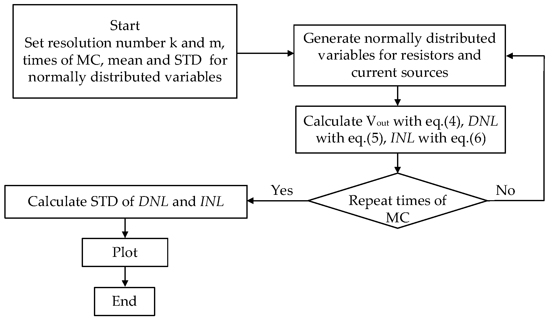
To evaluate the quantity of DNL and INL caused by the mismatch, a Monte Carlo (MC) simulation is performed based on Equations (4)–(6). The algorithm for a MC simulation is described in Figure 2 and as follows. First, (2m − 1) and one normally distributed unit current source are generated for the current-steering array and the current unit biasing the resistor divider, respectively. The normally distributed unit resistors are generated for the resistor divider and the feedback resistor, respectively. Second, using Equations (4)–(6) with the normally distributed units, we calculate the DNL and INL. Third, the first and second steps are repeated 1000 times.
Figure 3 shows the calculated standard deviation (STD) of the simulation results. To study the relationship between DNL/INL and the resolution number of k and m, in Figure 3a–c, we set the resistor units and current source units as normally distributed variables with an identical mean of 1 LSB and an identical STD, δ = ξ = 0.02 LSBs. At the same time, Figure 3a–c explores four sets of different values of k and m, (a1) k = 0, m = 10, (a2) k = 10, m = 0, (b) k = 4, m = 6, and (c) k = 8, m = 2. The results of (a1) and (a2) are the same, so they are plotted in Figure 3a. To study the impact of differences in the mismatch between the two device types (current sources and resistors) on the DNL/INL, Figure 3d explores three sets of different values of δ and ξ when k = 4 and m = 6. Figure 3 shows four variation phenomena of nonlinearity when the segmentation ratio k/m or (δ, ξ) vary.
- (1)
- For k = 0 or m = 0, as shown in Figure 3a, the maximum DNL and INL are the smallest compared with the other two sets of k and m. When k or m is zero, the DAC becomes a traditional R-DAC or I-DAC, not an R-I hybrid DAC, so the nonlinearity complies with the characteristic of the monotonic n-bit DAC, that is DNL = σ, INL = 0.5· · σ [13].
- (2)
- For nonzero k and m, as shown in Figure 3b,c, the maximum DNL happens at the transition when k bits of LSBs switch from 1 to 0 and add 1 to the MSBs, and happens 2m − 1 times. This phenomenon is caused by the segmented nature of the R-I DAC because the decoders for the R-subDAC and I-subDAC both adopt unary weighty control schemes.
- (3)
- For nonzero k and m, as shown in Figure 3b,c, the maximum DNL and INL increase with the increase of the segmentation ratio k/m. The reason will be discussed in the following section.
- (4)
- For (k, m) = (4, 6) and varying (δ, ξ), as shown in Figure 3d, the mismatch ξ in the current sources has more of an impact on the DNL/INL than the mismatch δ in the resisters. Specifically, the DNL/INL increases a little when (δ, ξ) varies from (0.02, 0.02) to (0.04, 0.02). The DNL/INL almost doubles when (δ, ξ) varies from (0.02, 0.02) to (0.02, 0.04). The reason will be discussed in the following section.
4. Theoretical Expressions to Depict the Nonlinearity Affected by Segmentation and the Matching Precision of the R-I DAC
Section 3 studied the nonlinearity mechanism by numeric simulation. In this section, the nonlinearities—DNL/INL—are theoretically derived.
We obtain Equation (7) by neglecting the product of the small variables in Equation (4)
4.1. DNL Analysis
Combining Equations (5) and (7), we can obtain Equation (8). Due to the segmented nature of the R-I DAC, the worst-case DNL occurs at the transition when k bits of LSBs switch from 1 to 0 and add 1 to the MSBs; for example, changing 00…00_11…11 to 00…01_00…00. By simplifying Equation (8), we can obtain Equation (9):
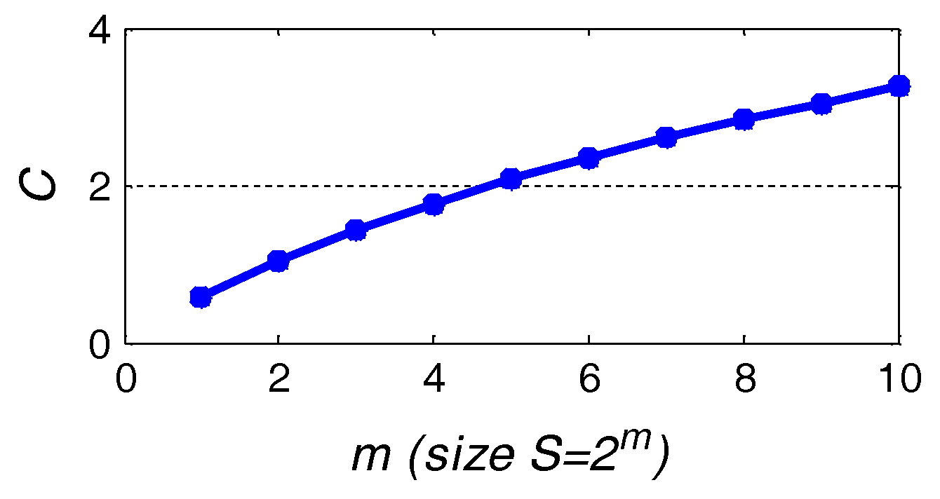
The DNL analysis aims to find the expected maximum DNL. Based on the extreme value theory, for the samples that are independent and identically distributed random variables, the largest individual from the samples of size S increases with size S [20]. Since samples X1, X2, …, XS are standard normal random variables, the expected value of maximum Xi (i from 1 to S, and S = 2m) is shown as C in Figure 4. Figure 4 is the result of a simulation as follows. First, we set the value of m and generate the 2m standard normal random samples. Second, we find their maximum and note it as Xi. Third, we repeat the previous two steps 10,000 times to get Xi (i from 1 to 10,000) for size 2m. Finally, we calculate the mean of Xi (i from 1 to 10,000); then, we note this mean as the expected maximum individual value C for samples of size 2m.
Since there are 2m samples of ξBHi in DNLMAX for BHi varying from 1 to 2m, the expected maximum ξBHi increases with 2m. So, the variance of ξBHi increases with m. Factor C describes the impact of m on the variance of the expected maximum value of ξBHi [18]. Factor C ranges from 1.02 to 3.25 when m varies from 2 to 10, and C = 2.3 for m = 6, as shown in Figure 4.
We get Equation (10) as the variance estimation of DNL in Equation (9):
In Equation (10), the σ2DNL1 is the variance estimation of DNL generated by the mismatches of the current units; the σ2DNL2 is the variance of DNL generated by the mismatches of the resistor units. The variance of DNL in Equation (10) increasing with the k explains the third variation phenomenon of nonlinearity in Figure 3 by theory. The factor in σ2DNL1 is greater than 2k times the factor in σ2DNL2, which indicates that the mismatch in the current array has a much greater effect on DNL than that in the resistors.
4.2. INL Analysis
With the approximation 2k − 1 ≈ 2k, 2m − 1 ≈ 2m, 2m+k − 1 ≈ 2m+k, the INL can be expressed as Equation (11), where INL1, INL2, INL3, and INL4 are the nonlinearities generated by the mismatches of the current-steering array, the feedback resistor, the resistor-divider biasing current, and the resistor-divider string, respectively.
Since the terms of INL are uncorrelated, the variance of INL is derived as Equation (12):
It is too complicated to derive the mathematical expression of the maximum variance of the total INL. However, it can be upper bounded by taking the worst case of each component. The maximum variance of the total INL is less than or equal to the sum of the maximum variance of each INL components, as shown in Equations (12)–(14). The approximation is valid only when an input that almost causes the max of all of the INL components exists. The approximation error is less than 0.3 LSB when k + m = 10 and k is smaller than 8, as shown in Figure 4.
where the maximum of each component in Equation (12) is derived as Equation (14).
Expressions (10) and (14) indicate that the nonlinearity roughly scales up by 22k + m of ξ2 and 2k of δ2. To directly understand its quantity level, the coefficients of theoretical variance of the differential nonlinearity (DNL) and integrated nonlinearity (INL) are calculated by using Equations (10) and (14), respectively, as shown in Table 1. The coefficient of DNL and INL both reach 100,000 when k increases to 8. The factor of ξ2 is approximately greater than 2k times of the factor of δ2. It indicates that the mismatch in the current array has a much greater effect on the nonlinearity than that in the resistors.
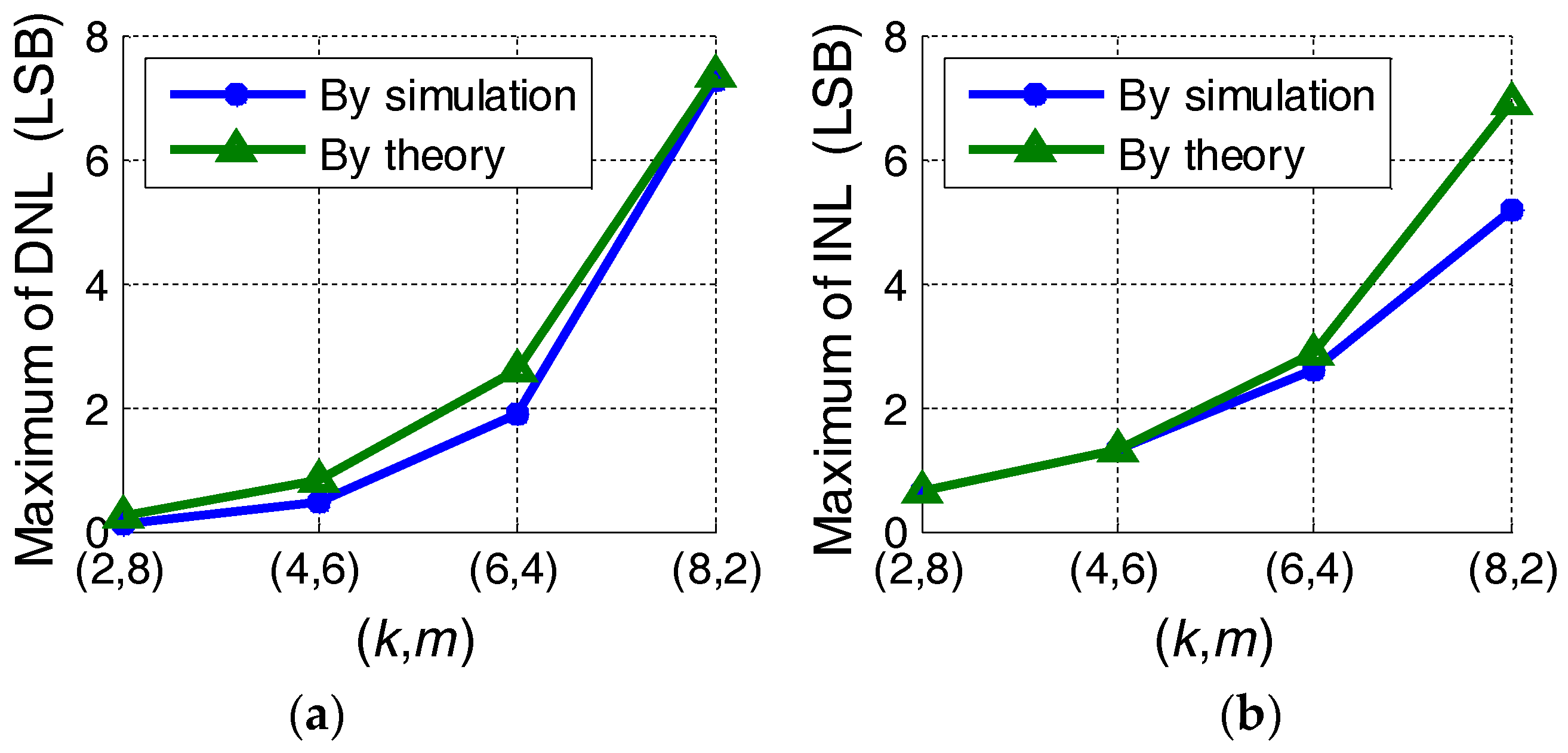
To verify the accuracy of the theoretical deviation, a comparison between the nonlinearity from the numeric simulation and the theoretical prediction equation is made, as shown in Figure 5. The nonlinearity by numeric simulation is obtained from Figure 3. The maximum nonlinearity by theory is calculated by Equations (10) and (14) with ξ and δ both being 0.02 LSBs. In Figure 5, except the INL difference when k is 8 and m is 2, other differences between the simulation and theory are less than 0.5 LSBs. Since the nonlinearity increases as a k exponent of two, a k of less than 6 is recommended for the matching consideration.
Previous analyses of DNL and INL gave the mathematical expressions to evaluate the nonlinearity with a specified matching resolution. The nonlinearity variance was approximately scaled up by 22k+m of ξ2 and 2k of δ2. In the actual design, the mismatching resolution is usually calculated from a given DNL and INL. Section 5 derives the expressions of matching resolution with a given worst nonlinearity.
5. Determination of the Segmentation and Matching Precision of the R-I DAC
The goal of this section is to derive the matching resolution of each mismatched component with a given worst DNL and INL that is smaller than half an LSB. Assuming that each component contributes equally to the nonlinearity, that is:
By simplifying Equation (15), we can obtain Equation (17). Similarly, by simplifying Equation (16), we can obtain Equation (18):
Combining Equations (17) and (18), the mismatching resolution can be expressed as Equations (19) and (20):
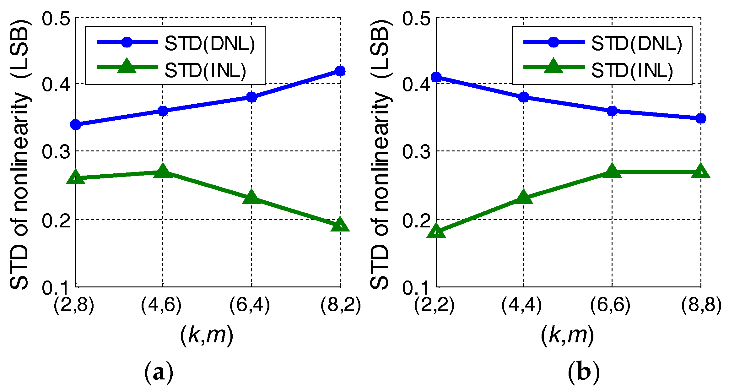
The expressions of matching resolution are obtained by ignoring some insignificant factors, such as the product of small variables in Equation (7). To verify its prediction accuracy of nonlinearity, the Monte Carlo simulation is performed in a similar way to that in Figure 3. The simulations are carried out by MATLAB using the normal random distribution for the unit variation of I-subDAC and R-subDAC. The variation has zero mean and a relative variance of ξ2 and δ2, respectively, as defined by equations (19) and (20). By repeating the previous Monte Carlo simulation 100,000 times, we obtain the standard deviation (STD) of the DNL_max and INL for different combinations of k and m. All of the standard deviations are calculated after 100,000 Monte Carlo runs except k = 8 and m = 8, where the number of runs is 1000. The STD of nonlinearity varies between 0.18–0.42 LSB, as shown in Figure 6. For all of the combinations of k and m, the maximum of STD nonlinearity is smaller than 0.5 LSB. This conforms to our matching resolution analysis.
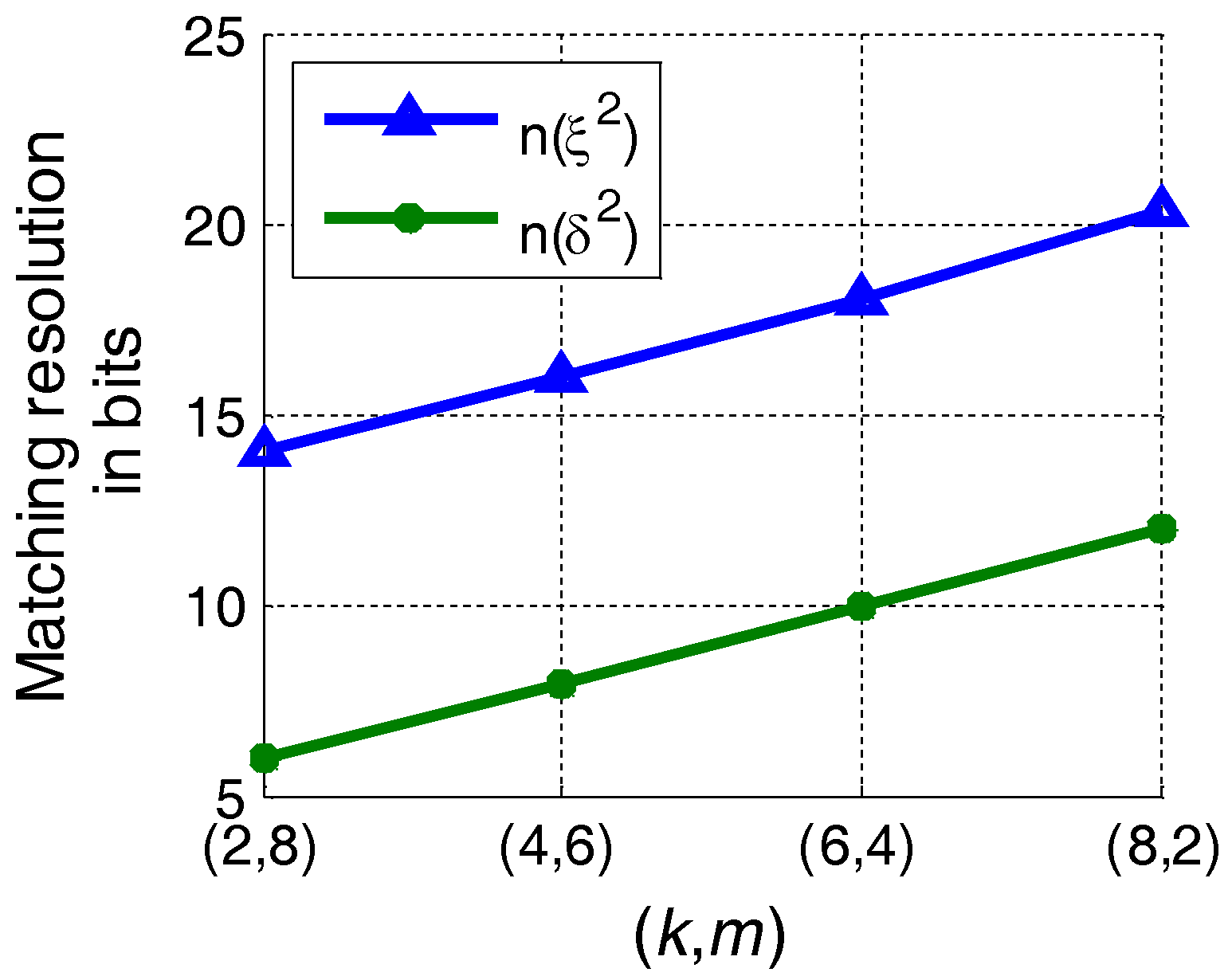
For the convenience of the description, the n(σ2) is defined as the matching resolution in bits, as a function of variance σ2 of matching precision, n(σ2) = log2(1/σ2). Using Equations (19) and (20), we can plot Figure 7.
When k + m = 10, we obtain n(ξ2) = 2k + m + 2 = n + k + 2 and n(δ2) = k + 4 approximately from Equations (19) and (20) and Figure 7, by assuming an equal contribution of the resistor and current source mismatching to nonlinearity. The expressions provide a criterion to design the mismatching precision of the I-subDAC and R-subDAC. The k is very influential on the matching resolution in bits for the I-subDAC. Since n(ξ2) is proportional to 2k, n(ξ2) increases greatly when k increases. To avoid too stringent matching requirements, it is recommended that k is less than 6.
6. Dynamic Performance Affected by the Segmentation and Matching Precision of R-I DAC
In previous sections, we discussed the relationship between the static nonlinearity DNL/INL and the segmentation, as well as the matching precision of the R-I DAC. The focus of this section is on how the segmentation and matching precision of the R-I DAC affects the dynamic nonlinearity.
One of the major factors in the dynamic performance is the static nonlinearities of DNL/INL. Besides the static nonlinearity, the other factors are glitches, timing mismatch errors, and some high-frequency parasitic parameters [21]. At a low frequency, the dynamic performance is mainly determined by the static nonlinearity, which does not scale with frequency. With the frequency increases, the glitches, timing mismatch errors, and some high-frequency parasitic parameters become more visible and dominant. So, the dynamic performance gets worse. Therefore, the static nonlinearity set an upper limit for the dynamic nonlinearity.
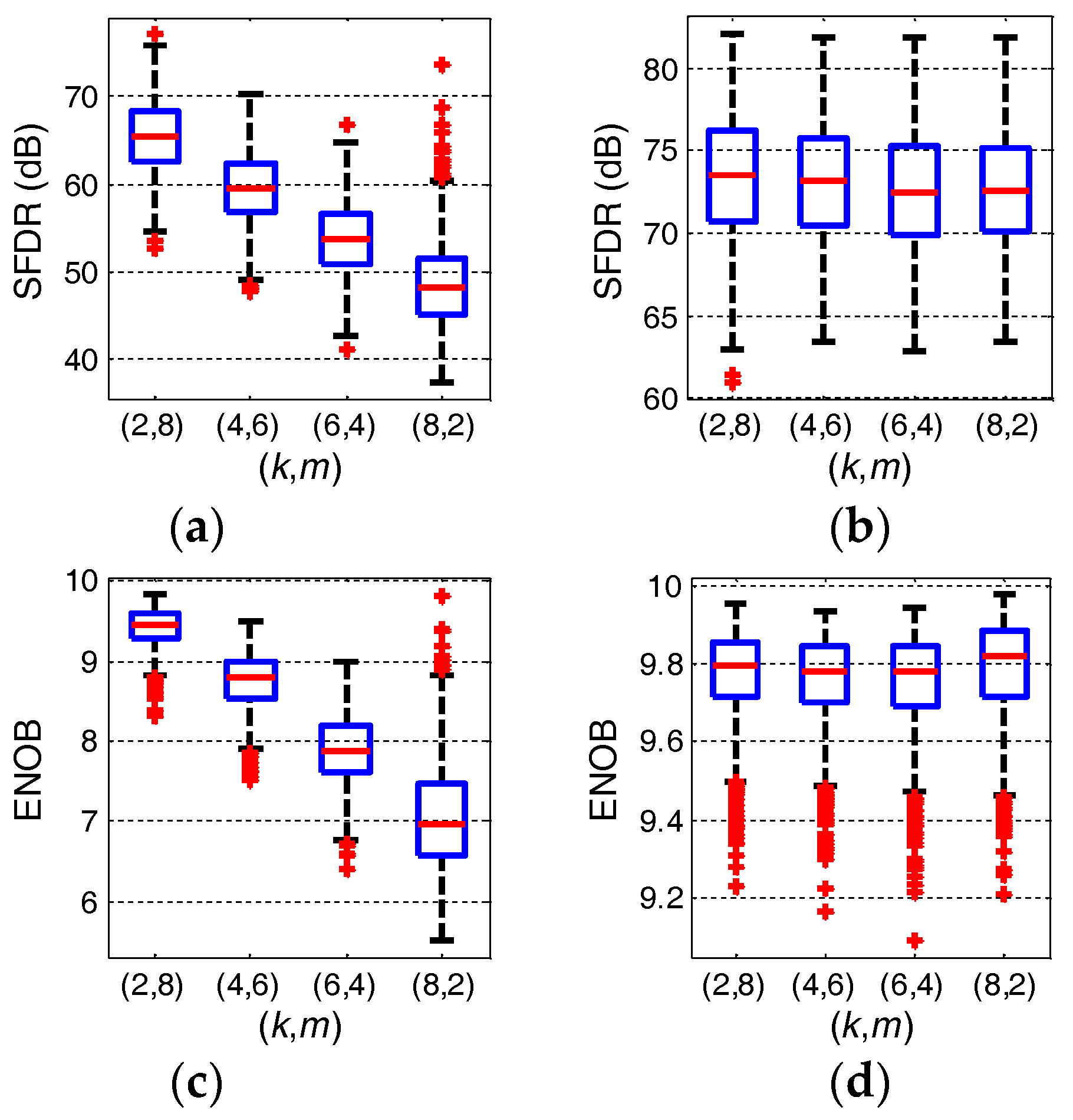
To evaluate the dynamic performance affected by segmentation and matching precision, a Monte Carlo simulation is performed in a similar way to that in Figure 3. Firstly, the matching accuracy of the resistor units and current-source units is set; then, the R-I DAC’s output is calculated by Equation (4). This output is used to generate a sine-wave, and its spurious-free dynamic range (SFDR) and the effective number of bits (ENOB) are calculated. At last, the simulations are repeated 1000 times, and the SFDR and ENOB are plotted using a “boxplot” [22]. Boxplot: on each box, the central mark is the median, the edges of the box are the 25th and 75th percentiles, and the highest and lowest whiskers correspond to approximately ±2.7σ and 99.3 coverage if the data are normally distributed. The results are shown in Figure 8.
In Figure 8a,c, the matching accuracy of the resistor units (δ) and current-source units (ξ) are set as constant values, both at 0.02. As a result, their SFDR and ENOB get worse, which is similar to the DNL/INL in Figure 3, when k increases and m decreases. In Figure 8a,c, the SFDR decreases from 65 dB to 48 dB, and the ENOB decreases from 9.5 bit to 7 bit, when k increases from 2 to 8 and m decreases from 8 to 2. The trend of the dynamic and static performance conform to the dynamic performance being limited by the static nonlinearity.
In contrast, SFDR and ENOB in Figure 8b,d remain constant, closing to the best theoretical achievable value with an increasing k and decreasing m. The SFDR is around 73 dB, and the ENOB is around 9.8 bits. The main reason is that in Figure 8b,d, the matching accuracy of resistor units and current-source units are set respectively as and . They are derived in Section 5, with a design goal of DNL/INL smaller than half an LSB. From Figure 8b,d, we can reach the conclusion that, with the proposed theoretical matching accuracy, the designed R-I DAC can not only achieve the static nonlinearity smaller than half an LSB, it can also assure the upper limit of the dynamic performance by being close to the best theoretically achievable value.
7. Implementation and Measurement for Verification
In the previous sections, simulations and theoretical derivation were used to analyze the nonlinearity affected by segmentation and mismatches. In this section, we discuss the design of the test chips using the proposed methodology.
Three test groups of prototypes of 10-bit (k = 4, m = 6) R-I DACs were implemented using the 180-nm standard complementary metal–oxide–semiconductor (CMOS) technology. These test chips groups only differed on the matching precision among the resistors and current sources in order to highlight the relationship between the matching precision and nonlinearity. Each test group had seven samples, and a total of 21 samples were under test.
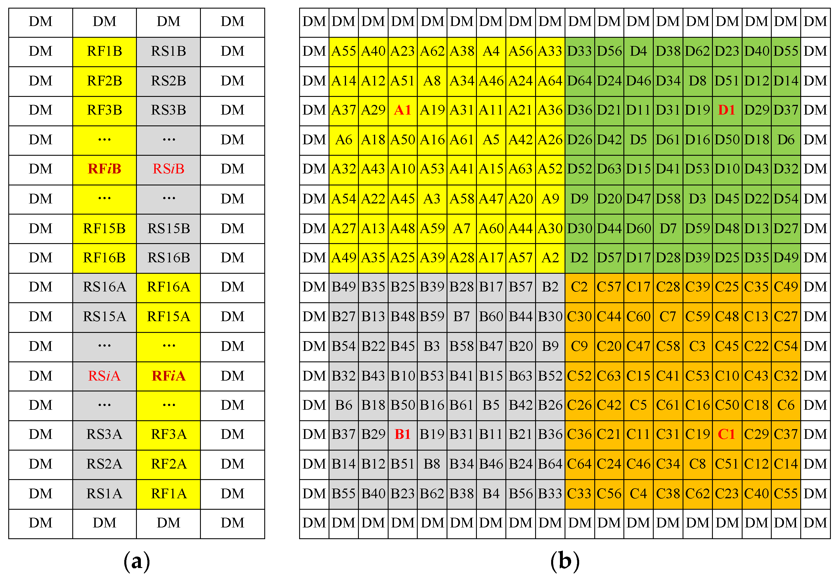
To attenuate the gradient-mismatch effects on nonlinearity, the common centroid and Q random layout skills were used in the resistors matching and current-sources matching, respectively, as shown in Figure 9 [5,23]. Similar to Reference [5], Q is referred to as one unit in every quadrant (A/B/C/D in Figure 9b), which altogether composed one current source in the layout. For example, current source 1 implemented by A1, B1, C1, and D1 in parallel. DM is the dummy unit. RSi and RFi are the unary resistor of the resistor-string (R-subDAC) and feedback resistor (RFB), respectively, where i is from 1 to 16. The “random” is not in the column or row sequence that was optimized to compensate for the quadratic-like residual errors.
In addition to the common-centroid layout, the sizing is another implementation consideration for matching precision [6,23]. Sizing the matching transistors (resistors) is a process of determining the value and the matching precision of the current (resistance). The value of the current (resistance) is a function of the width-to-length ratio (W/L), and the matching precision of the current (resistance) is a function of unary device size (W*L). So, the unary device shape, that is, the width and length, are determined by the value and the matching precision of the current (resistance). For resistors, the matching precision δ is provided by the proposed Equation (20), and the resistor size W*L is determined by the function W*L = aref/δ2, where aref is the reference resistor area provided by the foundry document for a 1% target precision [14]. The resistor length-to-width ratio is L/W = R/RS, where R is the designed resistance and RS is the sheet resistance. For the current source transistor, the matching precision ξ is provided by the proposed Equation (19), and the transistor size W*L is determined by the function , where VGS and VT are the gate-source voltage and the threshold voltage of a metal-oxide-semiconductor (MOS) transistor, respectively, and the mismatch of the technology parameters AVT2 and Aβ2 are 22 mV2 * μm2 and 0.04%* μm2 respectively, from the foundry document [6,14]. The transistor width to the length ratio is , where I and μnCox are the designed unary current and the I-V coefficient, respectively. The required resistor and transistor sizes of the R-I DAC are larger than that of the conventional segmented DAC architectures, because the requirement of the matching in the R-I DAC is more stringent.
The resistors were implemented by the high-sheet-resistance poly resistor, which was 1000 ohm/square. The resistance of the unit resistor is RU = 200 Ω. The matching precision due to the resistor size follows the guidelines of Reference [23]. The current source was implemented as a two-transistor cascode type. The matching precision due to the size of current source was determined with an INL yield model for the unary selection current-steering array [10,24]. The current of the unit current source was 5 μA. The overdrive voltage VGS-VT was set to 300 mV to compromise the current matching precision and transistor size [13,14,15]. The different matching precisions due to the size of the resistor (res-size) and the current source (cur-size) are listed in Table 2. The OP with an open-loop gain of 83 dB was adopted in our design. With such a large open-loop gain, the OP does not affect the precision and nonlinearity according to the analysis in Section 2. The test chips of group 1 and group 2 both used the large cur-size. Their measured nonlinearities are much better than the test group 3, in which a small cur-size was adopted. The chip bonding photos are shown in Figure 10.
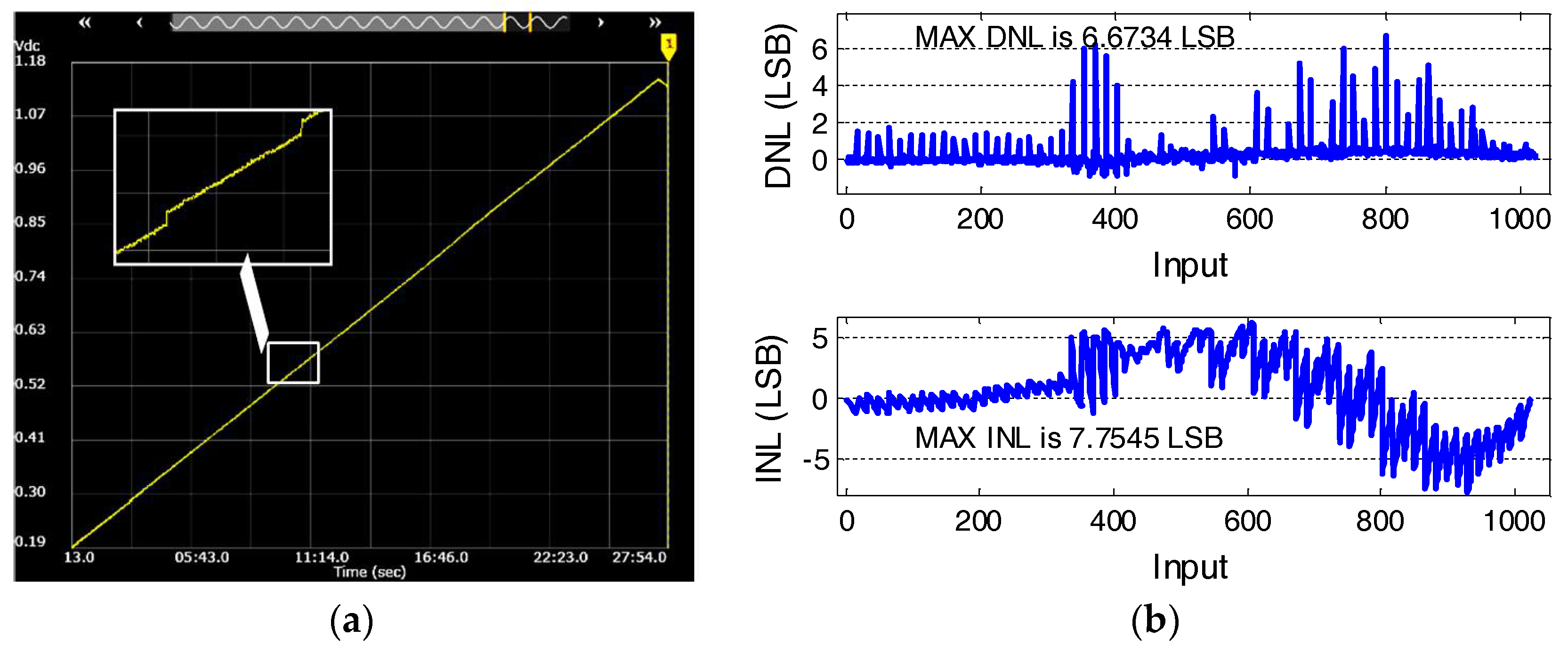
To test the proposed R-I DAC, the input data sequence was generated by a field-programmable gate array (FPGA) [3,24]. The output voltage was measured by a 6½-digit performance digital multimeter (DMM) Keysight-34461A. The output of test group 3, with an input of a full swing triangle wave, is shown in Figure 11. In Figure 11, the x-axis is time was proportional to the input, and the y-axis was the measured voltage. The magnified part shows the nonlinearity caused by the mismatching of the current-source transistors in test group 3.
The output voltage noise spectra density is measured by a spectrum analyzer (Rohde&Schwarz-FSV7), as shown in Figure 12 [25].
The DMM measurement precision is 3 μV with a 1.2-V input range. The measured low-frequency peak-to-peak noise voltage is 200 μV. This measurement of the noise floor determines the minimum measured absolute voltage, which limits the measured precision in Table 2. Since the measurement precision is 200 μV, it cannot measure the voltage below 200 μV. Therefore, for the actual measured voltage possibly less than 200 μV, we use 200 μV (worst-case value) to represent the measured value, which causes some error, but is acceptable for estimation.
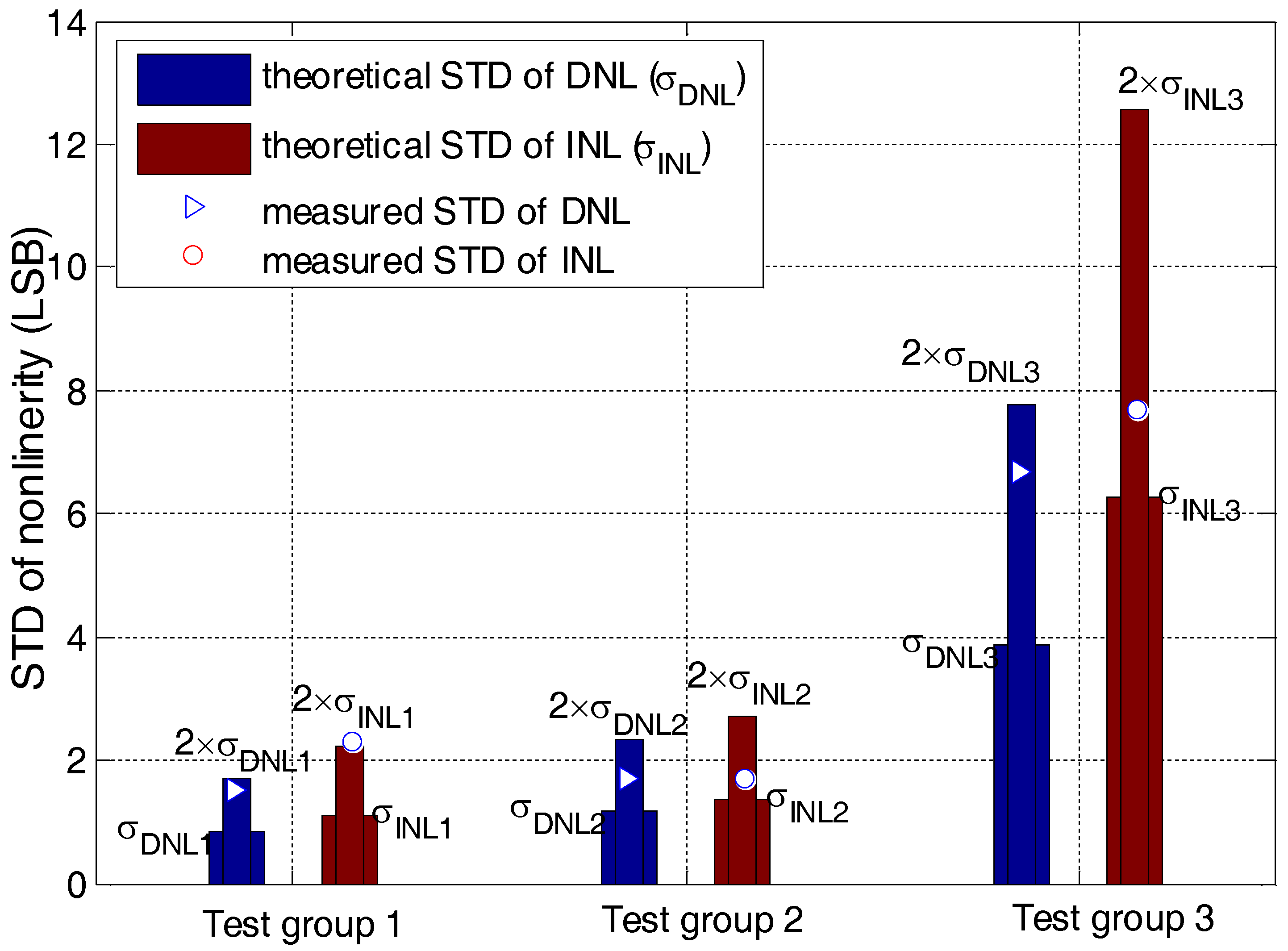
Using the measured relative precision variances in Table 2 and Equations (10) and (14), we can calculate the STD of nonlinearity. The calculated nonlinearity and the measured nonlinearity are plotted, as shown in Figure 13. The measured standard deviation of nonlinearity is less than two times that of the theoretical one, as shown in Figure 13. Since the nonlinearity is modeled as a normal probability distribution, the probability of one sample being less than two times the standard deviation is 95% [26]. Therefore, the difference between the measured results and the theoretical one falls within 95% of the normal distribution curve. In other words, our measured results match the theoretical ones in the statistical sense [26].
There is a discrepancy between the proposed theoretical STD of DNL/INL and the measured DNL/INL. The calculated STD of DNL/INL should be worse than the measured DNL/INL because, for test group 1 in Table 2, the measured precision of the resistors and current source are both worse than designed. However, the calculated STD of DNL/INL is better than the measured DNL/INL although their differences are insignificant, shown in Figure 13. The first reason is that if the matching resolution in bits n(ξ2) and n(δ2) are large enough, the variations of n(ξ2) and n(δ2) have little impact on the DNL/INL. For example, when n(δ2) is 6.3 and n(ξ2) varies from 12 to 14 and to 16, the DNL/INL varies from 0.89/1.2 to 0.70/0.80 and to 0.64/0.66. Therefore, the calculated STD of DNL/INL is not much worse. The second reason is that the measured DNL/INL is subject to the interference of the test environment, such as the power supply ripple and drifts of the reference voltage or current, especially when 1 LSB voltage is as small as 1 mV. So, the measured DNL/INL is slightly worse than expected. Therefore, the discrepancy is reasonable.
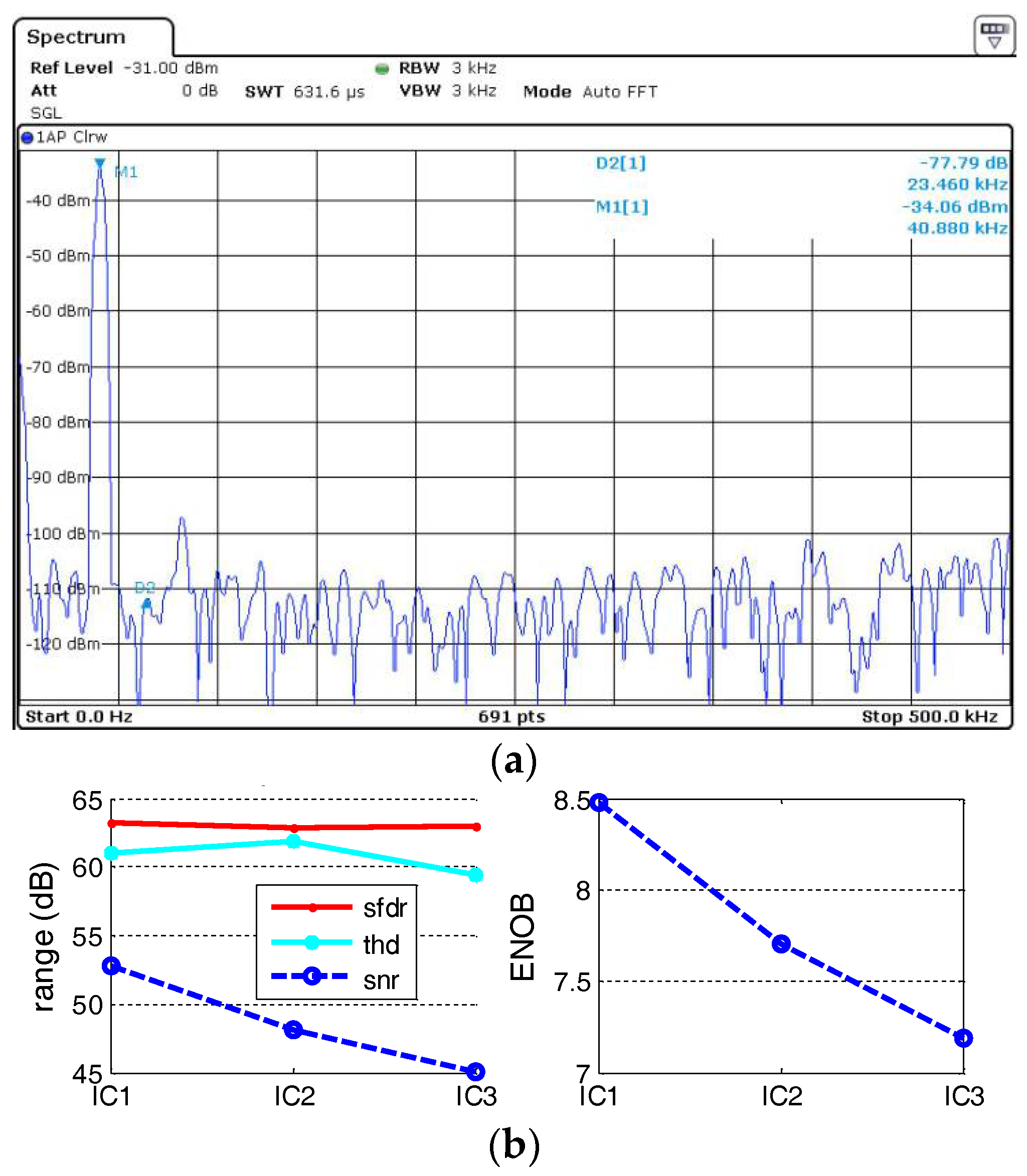
The measured dynamic performances are shown in Figure 14. The Rohde and Schwarz-FSV7 signal and spectrum analyzer measures the spectrum of the DAC output. The peak-to-peak voltage of the DAC sine-wave output is 1 V under a 1.35-V supply voltage. To avoid an overload effect on the spectrum analyzer, the DAC output is connected with the input of a spectrum analyzer through a series 4.7 kΩ resistor. Figure 14 is measured at a medium clock frequency and with a small input tone to stress the effect of segmentation and matching precision on the nonlinearity. Since the R-I DAC is designed for low-power applications, a low-power output operational amplifier (OP) is adopted, which limits the R-I DAC dynamic performance at high frequency. If the high-frequency and large input tones are used in the measurement, the poor high-frequency dynamic performance of the output OP overrides the effect of segmentation and matching precision on the nonlinearity. Therefore, the performance is measured at a medium clock frequency and with a small input tone to stress the focus of this article. Figure 14a shows the spectrum of the test group 1 with an input of a 40.88-kHz sine-wave at a clock frequency of 3.125 MHz. Figure 14b shows the dynamic performance, including the spurious-free dynamic range (SFDR), the total harmonic distortion (THD), the signal-to-noise ratio (SNR), and the effective number of bits (ENOB), of test groups 1–3. The SFDR of test groups 1–3 are around 65 dB, and the THD is around 60 dB. The differences of SFDR among test groups 1–3 are not obvious. The prime reason is the dynamic limitation of the low-power output of OP, which sets an upper limit of SFDR. Even though there is a limitation in OP, the THD of test group 3 is 2 dB less than that of test group 1, following the trend predicted in Section 6. The SNR and ENOB in Figure 14 decrease more obviously when the mismatch increases, as shown in Figure 13. The ENOB of test group 1 is 8.5 bits, which is 1.3 bits less than the one theoretically predicted by Figure 8d. It is reasonable because as a general rule, there is a 1-bit degradation in the measurement compared with the theoretical one [27].
In addition to nonlinearity, the sizing and power constraints also impact the choice of segmentation. When k increases and m decreases by 1 bit, the total resistor size quadruples, because both the resistor amount and the unary resistor size doubles. Meanwhile, the total size of the matching current source array stays the same, because the current source amount halves and the unary current source transistor size doubles. As a result, the total size of the R-I DAC increases dramatically if k is large. In addition, the large size increases the parasitics and degrades the speed. So, the sizing constraint limits the choice of a large k. In contrast, the power of the I-subDAC halves when k increases and m decreases by 1 bit, but the power reduction of the I-subDAC becomes unnecessary if the I-subDAC consumes a minority of the total power. The I-subDAC consumes less than a third of the total power in the implemented 10-bit (k = 4, m = 6) prototypes. So, further increasing k makes little contribution to the power reduction. In conclusion, the choice of segmentation should be compromised among the matching precision (for nonlinearity), total size, speed, and power, and a large k is not recommended.
Setting the values of the unary current and the unary resistor should compromise between the matching precision, size, and power. Lowering the unary current reduces the total power, but may result in a poor match, because the value and the matching precision together determine the unary device shape, that is, the width and length. The shape should follow the reliability guide of the layout to achieve the designed matching precision. In addition, there is a relationship between the current and resistor, as higher currents require lower resistors for the same output voltage. Therefore, after the matching precision specification is determined, the values of the unary current and the unary resistor should be simultaneously designed under the guidance of device sizing method and the layout reliability.
To verify the proposed methodology, three test groups differing on the matching precision among the resistors and current sources have been fabricated and tested. The measured results (Table 2 and Figure 13) are compared with the theoretical results for static nonlinearity (Equations (10) and (14)) and matching precision (Equations (19) and (20)). The verification supports the proposed prediction of nonlinearity by segmentation and matching precision. First, the resolution number of resistor (k) has more influence on the nonlinearity than the resolution number of current steering (m). Second, the nonlinearity gets worse when the segmentation ratio (k/m) increases. Finally, setting the matching resolution in bits of the resistors and current sources as k + 4 and m + 2k + 2, respectively, will obtain a DNL/INL that is smaller than half the LSBs.
8. Conclusions
Since the output of the R-I DAC is generated by the multiplication of the resistance and the current, the total mismatch gets amplified in a nonlinear way, which makes the accuracy analysis of the R-I DAC not as easy as that of conventional DACs. So, this article is motivated to interpret the numerical relationship between the nonlinearity and matching precision for the R-I DAC. In this article, we proposed a mathematical model that focused on the output and mismatches of the R-I DAC. To visualize the nonlinearity mechanism of the R-I DAC, we presented a simulation algorithm and illustrated the variation regularity of the nonlinearity. The regularity showed that the nonlinearity gets worse when the segmentation ratio (k/m) increases, and that the resolution number of resistor (k) has more influence on nonlinearity than the resolution number of current steering (m). In addition, we derived the theoretical expressions for static nonlinearity and matching precision. The numerical simulation and theoretical derivation concluded that the nonlinearity variance is proportional to the sum of 2kδ2 and 2n+kξ2. For a 10-bit R-I DAC, it is recommended that k is less than 6 to avoid matching requirements that are too stringent. When nonlinearity is required to be smaller than half an LSB, the matching resolution in bits of resistors and current sources are k + 4 and m + 2k + 2, respectively. The proposed theory is supported by the measured results of static and dynamic performance.
Author Contributions
Q.H. and F.Y. contributed to the main idea of this article; Q.H. performed the simulations, theoretical deviations, experiments and data analysis; Q.H. wrote the paper. F.Y. provided the funding, supervised the research, and revised the paper.
Acknowledgments
This work was supported in part by National key R&D plan (Grant number 2016YFC0105002 and 61674162), Shenzhen Key Lab for RF Integrated Circuits, Shenzhen Shared Technology Service Center for Internet of Things, Guangdong government funds (Grant numbers 2013S046 and 2015B010104005), Shenzhen government funds (Grant numbers JCYJ20160331192843950), and Shenzhen Peacock Plan.
Conflicts of Interest
The authors declare no conflict of interest.
Appendix A. Variable Notations
| Symbol | Definition |
| k | A k-bit resistor-string sub-DAC as LSBs |
| m | An m-bit current-steering sub-DAC as MSBs |
| n | An n-bit R-I hybrid DAC, n = k + m |
| IU, and IR | The unity current of the current source array, and the current through resistor-string, they are design to match, IU = IR. |
| RFB, and RU | Feedback resistance, and the unit resistance of resistor string, they are design to match, RFB = 2k·RU. |
| ΔIi (ΔRi), | A random absolute mismatch value ΔIi (ΔRi) |
| () | () Expected value |
| σ, ξ (δ) | The σ defines a general relative mismatch. The ξ(δ) is a specific random relative mismatch () |
| i | A digital input for R-I DAC with a decimal value |
| BLi and BHi | The digital input codes for R-sub DAC and I-sub DAC, respectivelyB = floor(A) rounds the elements of A to the nearest integers less than or equal to A. M = mod(X, Y) returns the modulus after division of X by Y. |
| bx | The bx represents one bit of the digital input code, where a bigger x indicates the more significant value of the bit. |
| n(σ2) | The matching precision in bits, as a function of variance σ2 of matching precision, n(σ2) = log2(1/σ2). |
References
- Van de Plassche, R.J. Cmos Integrated Analog-to-Digital and Digital-to-Analog Converters; Springer Science & Business Media: Berlin, Germany, 2013; Volume 742. [Google Scholar]
- Maloberti, F. Data Converters; Springer: Berlin, Germany, 2010. [Google Scholar]
- IEEE. IEEE Standard for Terminology and Test Methods of Digital-to-Analog Converter Devices; IEEE Std 1658-2011; IEEE: Piscataway, NJ, USA, 2012; pp. 1–126. [Google Scholar]
- Surkanti, P.R.; Mehrotra, D.; Gangineni, M.; Furth, P.M. Multi-String Led Driver with Accurate Current Matching and Dynamic Cancellation of Forward Voltage Mismatch. In Proceedings of the 2017 IEEE 60th International Midwest Symposium on Circuits and Systems (MWSCAS), Boston, MA, USA, 6–9 August 2017; pp. 229–232. [Google Scholar]
- Van Der Plas, G.A.M.; Vandenbussche, J.; Sansen, W.; Steyaert, M.S.J.; Gielen, G.G.E. A 14-bit intrinsic accuracy q2 random walk cmos dac. IEEE J. Solid-State Circuits 1999, 34, 1708–1718. [Google Scholar] [CrossRef]
- Pelgrom, M.J.M.; Duinmaijer, A.C.J.; Welbers, A.P.G. Matching properties of mos transistors. IEEE J. Solid-State Circuits 1989, 24, 1433–1439. [Google Scholar] [CrossRef]
- Lakshmikumar, K.R.; Hadaway, R.A.; Copeland, M.A. Characterisation and modeling of mismatch in mos transistors for precision analog design. IEEE J. Solid-State Circuits 1986, 21, 1057–1066. [Google Scholar] [CrossRef]
- Conroy, C.S.G.; Lane, W.A.; Moran, M.A.; Lakshmikumar, K.R.; Copeland, M.A.; Hadaway, R.A. Comments, with reply, on ‘characterization and modeling of mismatch in mos transistors for precision analog design’. IEEE J. Solid-State Circuits 1988, 23, 294–296. [Google Scholar] [CrossRef]
- Conroy, C.S.G.; Lane, W.A.; Moran, M.A. Statistical design techniques for d/a converters. IEEE J. Solid-State Circuits 1989, 24, 1118–1128. [Google Scholar] [CrossRef]
- Van den Bosch, A.; Steyaert, M.; Sansen, W. An Accurate Statistical Yield Model for Cmos Current-Steering d/a Converters. In Proceedings of the 2000 IEEE International Symposium on Circuits and Systems, Geneva, Switzerland, 28–31 May 2000; Volume 104, pp. 105–108. [Google Scholar]
- Kosunen, M.; Vankka, J.; Teikari, F.; Halonen, K. Dnl and inl Yield models for a current-steering d/a converter. In Proceedings of the International Symposium on Circuits and Systems, Bangkok, Thailand, 25–28 May 2003; Volume 961, pp. I:969–I:972. [Google Scholar]
- Rafeeque, K.P.S.; Vasudevan, V. A new technique for on-chip error estimation and reconfiguration of current-steering digital-to-analog converters. IEEE Trans. Circuits Syst. I 2005, 52, 2348–2357. [Google Scholar] [CrossRef]
- Baker, R.J. Cmos Circuit Design, Layout, and Simulation, 3rd ed.; Wiley-IEEE Press: Hoboken, NJ, USA, 2010; pp. 1231–1232. [Google Scholar]
- Ma, B.; Huang, Q.; Yu, F. A 12-bit 1.74-mw 20-ms/s dac with resistor-string and current-steering hybrid architecture. In Proceedings of the 2015 28th IEEE International, System-on-Chip Conference (SOCC), Beijing, China, 8–11 September 2015; pp. 1–6. [Google Scholar]
- Chi-Hung, L.; Bult, K. A 10-b, 500-msample/s cmos dac in 0.6 mm2. IEEE J. Solid-State Circuits 1998, 33, 1948–1958. [Google Scholar] [CrossRef]
- Seung-Tae, K.; Oh-Kyong, K. Small-area dac using adaptive body bias scheme for amoled data driver ics. Electron. Lett. 2015, 51, 1322–1324. [Google Scholar]
- Geunyeong, P.; Minkyu, S. A cmos current-steering d/a converter with full-swing output voltage and a quaternary driver. IEEE Trans. Circuits Syst. II 2015, 62, 441–445. [Google Scholar]
- Instruments, T. Products for Digital to Analog Converter. Available online: http://www.ti.com/lsds/ti/data-converters/digital-to-analog-converter-products.page (accessed on 1 May 2016).
- Knausz, I.; Bowman, R.J. A low power, scalable, dac architecture for liquid crystal display drivers. IEEE J. Solid-State Circuits 2009, 44, 2402–2410. [Google Scholar] [CrossRef]
- Tippett, L.H.C. On the extreme individuals and range of samples taken from a normal population. Biometrika 1925, 17, 364–387. [Google Scholar] [CrossRef]
- Yongjian, T.; Briaire, J.; Doris, K.; van Veldhoven, R.; van Beek, P.C.W.; Hegt, H.J.A.; van Roermund, A.H.M. A 14 bit 200 ms/s dac with sfdr > 78 dbc, im3 <-83 dbc and nsd < 163 dbm/hz across the whole nyquist band enabled by dynamic-mismatch mapping. IEEE J. Solid-State Circuits 2011, 46, 1371–1381. [Google Scholar]
- Matlab-R2017b. Boxplot. Available online: http://cn.mathworks.com/help/stats/boxplot.html (accessed on 20 December 2017).
- Hastings, A. The Art of Analog Layout, 2nd ed.; Pearson: London, UK, 2006. [Google Scholar]
- Huang, Q.; Yu, F. A high output swing current-steering dac using voltage controlled current source. Microelectron. J. 2017, 68, 32–39. [Google Scholar] [CrossRef]
- Kay, A. Operational Amplifier Noise: Techniques and Tips for Analyzing and Reducing Noise; Elsevier: Amsterdam, The Netherlands, 2012. [Google Scholar]
- Stark, H.; Woods, J.W. Probability, Statistics, and Random Processes for Engineers; Pearson: London, UK, 2012. [Google Scholar]
- Sansen, W.M.C. Analog Design Essentials; Springer: Berlin, Germany, 2006. [Google Scholar]
Figure 1.
The k + m bits resistor-string and current-steering-array hybrid DAC (R-I DAC) with the resistor’s and current’s mismatches.
Figure 1.
The k + m bits resistor-string and current-steering-array hybrid DAC (R-I DAC) with the resistor’s and current’s mismatches.

Figure 2.
The algorithm of simulation.

Figure 3.
The standard deviation (STD) of differential nonlinearity (DNL) and integrated nonlinearity (INL) of 1000 Monte Carlo MATLAB simulations. (a–c) show the results when δ = ξ = 0.02 and segmentation (k/m) varies: (a) k = 0, m = 10 or k = 10, m = 0, (b) k = 4, m = 6, (c) k = 8, m = 2. (d) is the maximum STD of DNL and INL when k = 4, m = 6, and (δ, ξ) varies.

Figure 4.
The expected value C of the maximum individual from samples of size S = 2m, in which the samples are standard normal random variables.
Figure 4.
The expected value C of the maximum individual from samples of size S = 2m, in which the samples are standard normal random variables.

Figure 5.
A comparison between the maximum nonlinearity from the numerical simulation and theoretical prediction equation. (a) DNL, (b) INL.
Figure 5.
A comparison between the maximum nonlinearity from the numerical simulation and theoretical prediction equation. (a) DNL, (b) INL.

Figure 6.
The predicted standard deviation (STD) of DNL and INL for different combinations of k and m for 100,000 Monte Carlo runs, using the matching resolution defined by Equations (19) and (20). (a) The (k + m = 10) bit resolution of the R-I DAC. (b) k = m and K + M ranging from 4 to 16.
Figure 6.
The predicted standard deviation (STD) of DNL and INL for different combinations of k and m for 100,000 Monte Carlo runs, using the matching resolution defined by Equations (19) and (20). (a) The (k + m = 10) bit resolution of the R-I DAC. (b) k = m and K + M ranging from 4 to 16.

Figure 7.
The matching resolution in bits for the different combinations of k and m for n = k + m = 10 by assuming that each component contributes equally to the nonlinearity.
Figure 7.
The matching resolution in bits for the different combinations of k and m for n = k + m = 10 by assuming that each component contributes equally to the nonlinearity.

Figure 8.
With the different matching accuracy among the resistor units and among the current-source units, the boxplot of spurious-free dynamic range (SFDR) (a,b) and the effective number of bits (ENOB) (c,d) of a 1000 Monte Carlo MATLAB simulations when k and m vary. In (a,c), δ = ξ = 0.02. In (b,d), and , respectively.

Figure 9.
The common-centroid layout of (a) matching resistors, unary resistor RSi (RFi) implemented as two units in red—RSiA (RFiA), and RSiB (RFiB)—in series, where the background color of RSiA (RSiB) and RFiA (RFiB) are gray and yellow, respectively, and (b) matching the current sources, unary current sources implemented as four units (A, B, C, and D with background color of yellow, gray, orange and green, respectively) in parallel. For example, current source 1 consists of A1, B1, C1 and D1 in red. DM is the dummy unit.

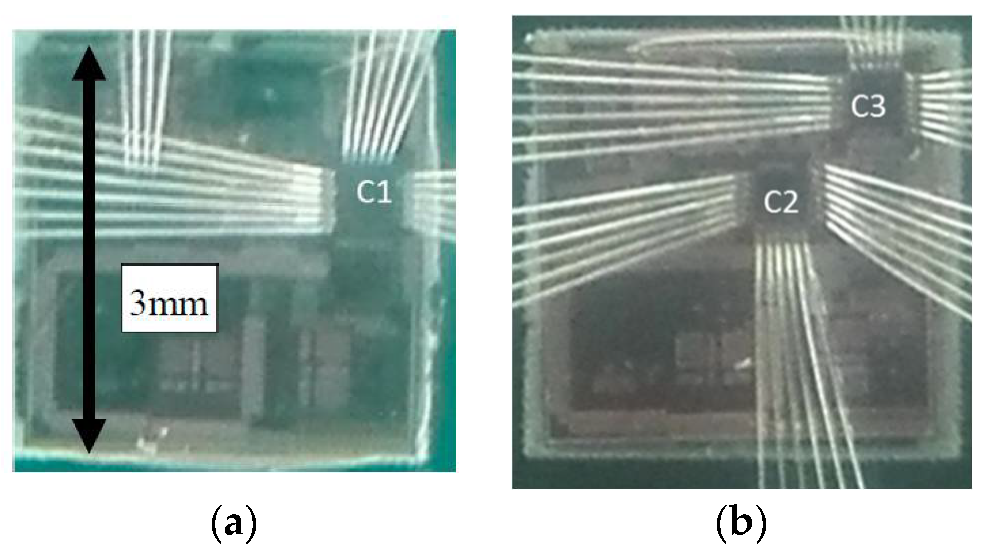
Figure 10.
The chip-bonding photos of (a) test group 1; (b) test group 2; and test group 3.

Figure 11.
(a) The measured output of test group 3 with an input of a full swing triangle wave. (b) The static nonlinearity DNL/INL of the measured output versus the digital input, a result of Figure 11a.
Figure 11.
(a) The measured output of test group 3 with an input of a full swing triangle wave. (b) The static nonlinearity DNL/INL of the measured output versus the digital input, a result of Figure 11a.

Figure 12.
Output voltage noise spectra density measured results.

Figure 13.
The comparison between the theoretical calculated nonlinearity and the measured nonlinearity. The theoretical calculation of nonlinearity is computed using the measured relative precision variances in Table 2 and Equations (10) and (14).
Figure 13.
The comparison between the theoretical calculated nonlinearity and the measured nonlinearity. The theoretical calculation of nonlinearity is computed using the measured relative precision variances in Table 2 and Equations (10) and (14).

Figure 14.
(a) The measured spectrum of test group 1, with an input of a 40.88 kHz sine-wave at a clock frequency of 3.125 MHz. (b) The measured dynamic performance including spurious-free dynamic range (SFDR), the total harmonic distortion (THD), the signal-to-noise ratio (SNR), and the effective number of bits (ENOB) of test groups 1–3 under the identical test environment, as in Figure 11a.


Table 1.
The quantity comparison of theoretical variance of DNL and INL for different sets of k and m for a 10-bit R-I DAC.
Table 1.
The quantity comparison of theoretical variance of DNL and INL for different sets of k and m for a 10-bit R-I DAC.
| Variance | k = 2, m = 8 | k = 4, m = 6 | k = 6, m = 4 | k = 8, m = 2 |
|---|---|---|---|---|
| σ2DNL | 139ξ2 + 7δ2 | 1629ξ2 + 31δ2 | 16735ξ2 + 127δ2 | 134608ξ2 + 511δ2 |
| σ2INL | 1040ξ2 + 6.2δ2 | 4348ξ2 + 30δ2 | 20232ξ2 + 118δ2 | 118656ξ2 + 398δ2 |
Table 2.
The different sizes of resistors and current-source results in different measured nonlinearities.
Table 2.
The different sizes of resistors and current-source results in different measured nonlinearities.
| Test Chip Group | Size of Matching (Multiplier × W × L, the Unit is μm × μm) | Designed Precision (Absolute Voltage, Relative Precision Variance) | Measured Precision (Absolute Voltage, Relative Precision Variance) | Measured Nonlinearity (DNL and INL in LSB, Relative Precision) |
|---|---|---|---|---|
| Test group 1 (large res-size, large cur-size) | Resistor size (2 × 2 × 29.78) | 62.5 μV, 1/28 | 200 μV, 1/26.3 | 1.5 and 2.3, 1/29.4 and 1/28.8 |
| Current-source transistor size (4 × 4.42 × 50) | 28 μV, 1/215.1 | 200 μV, 1/212.3 | ||
| Test group 2 (small res-size, large cur-size) | Resistor size (2 × 0.8 × 11.605) | 250 μV, 1/26 | 540 μV, 1/24.9 | 1.7 and 1.7, 1/29.2 and 1/29.2 |
| Current-source transistor size (4 × 4.42 × 50) | 28 μV, 1/215.1 | 200 μV, 1/212.3 | ||
| Test group 3 (large res-size, small cur-size) | Resistor size (2 × 2 × 29.78) | 62.5 μV, 1/28 | 200 μV, 1/26.3 | 6.7 and 7.7, 1/27.2 and 1/27.0 |
| Current-source transistor size (4 × 0.375 × 4.245) | 16 mV, 1/26 | 9 mV, 1/26.8 |
© 2018 by the authors. Licensee MDPI, Basel, Switzerland. This article is an open access article distributed under the terms and conditions of the Creative Commons Attribution (CC BY) license (http://creativecommons.org/licenses/by/4.0/).
Share and Cite
MDPI and ACS Style
Huang, Q.; Yu, F. Prediction of the Nonlinearity by Segmentation and Matching Precision of a Hybrid R-I Digital-to-Analog Converter. Electronics 2018, 7, 91. https://doi.org/10.3390/electronics7060091
AMA Style
Huang Q, Yu F. Prediction of the Nonlinearity by Segmentation and Matching Precision of a Hybrid R-I Digital-to-Analog Converter. Electronics. 2018; 7(6):91. https://doi.org/10.3390/electronics7060091
Chicago/Turabian StyleHuang, Qinjin, and Fengqi Yu. 2018. "Prediction of the Nonlinearity by Segmentation and Matching Precision of a Hybrid R-I Digital-to-Analog Converter" Electronics 7, no. 6: 91. https://doi.org/10.3390/electronics7060091
Note that from the first issue of 2016, this journal uses article numbers instead of page numbers. See further details here.